LIFETIME BUY
The MC74F257 is a quad 2-input multiplexer with 3-state outputs. Four bits
of data from two sources can be selected using a common Data Select input.
The four outputs present the selected data in true (non-inverted) form. The
outputs may be switched to a high impedance state with a HIGH on the common Output Enable (OE) input, allowing the outputs to interface directly with
bus oriented systems.
• Multiplexer Expansion by Tying Outputs Together
• Non-Inverting 3-State Outputs
• Input Clamp Diodes Limit High-Speed Termination Effects
• AC Enhanced Version of the F257
QUAD 2-INPUT MULTIPLEXER
WITH 3-STATE OUTPUTS
FAST SCHOTTKY TTL
J SUFFIX
CERAMIC
CASE 620-09
CONNECTION DIAGRAM
VCC
OE
I0c
I1c
Zc
I0d
I1d
Zd
16
15
14
13
12
11
10
9
16
1
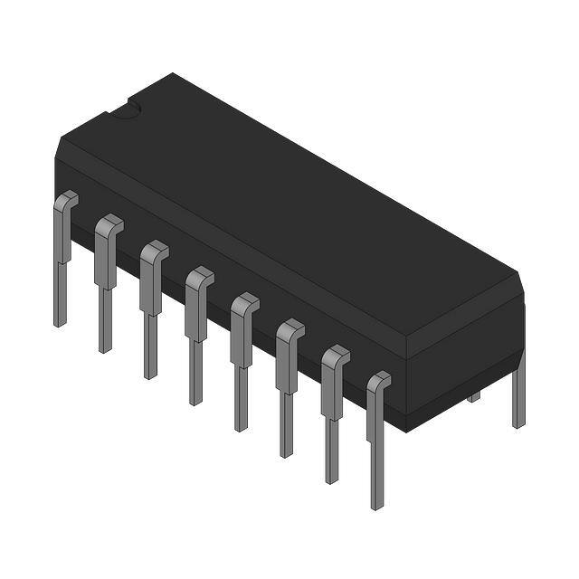
N SUFFIX
PLASTIC
CASE 648-08
16
1
2
3
4
5
6
7
8
S
I0a
I1a
Za
I0b
I1b
Zb
GND
I1c
I0d
1
LOGIC DIAGRAM
OE
I0a
I1a
I0b
I1b
I0c
I1d
D SUFFIX
SOIC
CASE 751B-03
S
16
1
ORDERING INFORMATION
MC54FXXXAJ Ceramic
MC74FXXXAN Plastic
MC74FXXXAD SOIC
LOGIC SYMBOL
1
Za
Zb
Zc
S
Zd
Select
Input
OE
S
Data
Inputs
Outputs
H
X
I0
X
I1
X
Z
L
H
X
L
L
L
H
X
H
H
7
Zb
I0b
I1b
12
Zc
I0c
14
9
I1c
I0d
13
Zd
I1d
L
L
L
X
L
10
L
L
H
X
H
Z
H = HIGH Voltage Level
L = LOW Voltage Level
X = Don’t Care
Z = High Impedance
VCC = PIN 16
GND = PIN 8
15
Za
FUNCTION TABLE
Output
Enable
OE
I0a
I1a
4
2
3
5
6
11
LAST SHIP 30/09/99
QUAD 2-INPUT MULTIPLEXER
WITH 3-STATE OUTPUTS
LAST ORDER 31/03/99
MC74F257A
�GUARANTEED OPERATING RANGES
Parameter
Min
Typ
Max
Unit
VCC
Supply Voltage
74
4.5
5.0
5.5
V
TA
Operating Ambient Temperature Range
74
0
25
70
°C
IOH
Output Current — High
74
–3.0
mA
IOL
Output Current — Low
74
24
mA
DC CHARACTERISTICS OVER OPERATING TEMPERATURE RANGE (unless otherwise specified)
Limits
LIFETIME BUY
Symbol
Parameter
VIH
Input HIGH Voltage
VIL
Input LOW Voltage
VIK
Input Clamp Diode Voltage
VOH
Output HIGH Voltage
Min
Typ
Max
2.0
Unit
Test Conditions
V
Guaranteed Input HIGH Voltage
0.8
V
Guaranteed Input LOW Voltage
–1.2
V
IIN = –18 mA
VCC = MIN
74
2.4
3.3
V
IOH = –3.0 mA
VCC = 4.50 V
74
2.7
3.3
V
IOH = –3.0 mA
VCC = 4.75 V
0.5
V
IOL = 24 mA
VCC = MIN
VOL
Output LOW Voltage
0.35
IOZH
Output OFF Current — HIGH
50
µA
VOUT = 2.7 V
VCC = MAX
IOZL
Output OFF Current — LOW
–50
µA
VOUT = 0.5 V
VCC = MAX
IIH
Input HIGH Current
20
µA
VIN = 2.7 V
VCC = MAX
100
IIL
Input LOW Current
IOS
Output Short Circuit Current (Note 2)
–60
ICCH
9.0
VIN = 7.0 V
–0.6
mA
VIN = 0.5 V
VCC = MAX
–150
mA
VOUT = 0 V
VCC = MAX
15
S, I1x = 4.5 V
OE, I0x = GND
ICCL
Power Supply Current
14.5
22
mA
I1x = 4.5 V
VCC = MAX
OE, I0x, S = GND
ICCZ
15
23
S, I0x = GND
OE, I1x = 4.5 V
NOTES:
1. For conditions shown as MIN or MAX, use the appropriate value specified under guaranteed operating ranges.
2. Not more than one output should be shorted at a time, nor for more than 1 second.
FUNCTIONAL DESCRIPTION
The F257A is a quad 2-input multiplexer with 3-state outputs. It selects four bits of data from two sources under control
of a Common Data Select input. When the Select input is
LOW, the I0x inputs are selected and when Select is HIGH, the
I1x inputs are selected. The data on the selected inputs appears at the outputs in true (non-inverted) form. The device is
the logic implementation of a 4-pole, 2-position switch where
the position of the switch is determined by the logic levels supplied to the Select input. The logic equations for the outputs
are shown below:
Za = OE • (I1a • S + I0a • S)
Zb = OE • (I1b • S + I0b • S)
Zc = OE • (I1c • S + I0c • S)
Zd = OE • (I1d • S + I0d • S)
When the Output Enable input (OE) is HIGH, the outputs are
forced to a high impedance OFF state. If the outputs are tied
together, all but one device must be in the high impedance
state to avoid high currents that would exceed the maximum
ratings. Designers should ensure the Output Enable signals
to 3-state devices whose outputs are tied together are designed so there is no overlap.
LAST ORDER 31/03/99
Symbol
LAST SHIP 30/09/99
MC74F257A
�LIFETIME BUY
Symbol
Parameter
74F
74F
TA = +25°C
TA = 0°C to 70°C
VCC = +5.0 V
VCC = 5.0 V ± 10%
CL = 50 pF
CL = 50 pF
Min
Max
Min
Max
Unit
6.0
ns
tPLH
Propagation Delay
1.5
5.5
1.5
tPHL
In to Zn
2.0
5.5
2.0
6.0
tPLH
Propagation Delay
3.0
9.5
3.0
10.5
tPHL
S to Zn
2.5
7.0
2.5
8.0
tPZH
Output Enable Time
2.0
6.5
2.0
7.0
2.5
7.0
2.5
8.0
2.0
6.0
2.0
7.0
2.0
6.0
2.0
7.0
tPZL
tPHZ
tPLZ
Output Disable Time
ns
ns
ns
LAST ORDER 31/03/99
AC CHARACTERISTICS
LAST SHIP 30/09/99
MC74F257A
�LAST SHIP 30/09/99
Motorola reserves the right to make changes without further notice to any products herein. Motorola makes no warranty, representation or
guarantee regarding the suitability of its products for any particular purpose, nor does Motorola assume any liability arising out of the application
or use of any product or circuit, and specifically disclaims any and all liability, including without limitation consequential or incidental damages.
“Typical” parameters which may be provided in Motorola data sheets and/or specifications can and do vary in different applications and actual
performance may vary over time. All operating parameters, including “Typicals” must be validated for each customer application by customer’s
technical experts. Motorola does not convey any license under its patent rights nor the rights of others. Motorola products are not designed,
intended, or authorized for use as components in systems intended for surgical implant into the body, or other applications intended to support
or sustain life, or for any other application in which the failure of the Motorola product could create a situation where personal injury or death
may occur. Should Buyer purchase or use Motorola products for any such unintended or unauthorized application, Buyer shall indemnify and
hold Motorola and its officers, employees, subsidiaries, affiliates, and distributors harmless against all claims, costs, damages, and expenses,
and reasonable attorney fees arising out of, directly or indirectly, any claim of personal injury or death associated with such unintended or
unauthorized use, even if such claim alleges that Motorola was negligent regarding the design or manufacture of the part. Motorola and
are registered trademarks of Motorola, Inc. Motorola, Inc. is an Equal Opportunity/Affirmative Action Employer.
How to reach us:
USA/EUROPE/Locations Not Listed: Motorola Literature Distribution; P.O. Box 5405, Denver, Colorado 80217.
1–303–675–2140 or 1–800–441–2447
JAPAN: Motorola Japan Ltd.; SPS, Technical Information Center, 3–20–1, Minami–Azabu. Minato–ku, Tokyo 106–8573 Japan.
81–3–3440–3569
ASIA/PACIFIC: Motorola Semiconductors H.K. Ltd.; Silicon Harbour Centre, 2 Dai King Street, Tai Po Industrial Estate, Tai Po,
N.T., Hong Kong. 852–26668334
Customer Focus Center: 1–800–521–6274
Mfax: RMFAX0@email.sps.mot.com
– TOUCHTONE 1–602–244–6609
Motorola Fax Back System
– US & Canada ONLY 1–800–774–1848
– http://sps.motorola.com/mfax/
HOME PAGE: http://motorola.com/sps/
◊
LAST ORDER 31/03/99
LIFETIME BUY
Mfax is a trademark of Motorola, Inc.
�


 工商网监
湘ICP备2023018690号
工商网监
湘ICP备2023018690号
