ON Semiconductor
Is Now
To learn more about onsemi™, please visit our website at
www.onsemi.com
onsemi and and other names, marks, and brands are registered and/or common law trademarks of Semiconductor Components Industries, LLC dba “onsemi” or its affiliates and/or
subsidiaries in the United States and/or other countries. onsemi owns the rights to a number of patents, trademarks, copyrights, trade secrets, and other intellectual property. A listing of onsemi
product/patent coverage may be accessed at www.onsemi.com/site/pdf/Patent-Marking.pdf. onsemi reserves the right to make changes at any time to any products or information herein, without
notice. The information herein is provided “as-is” and onsemi makes no warranty, representation or guarantee regarding the accuracy of the information, product features, availability, functionality,
or suitability of its products for any particular purpose, nor does onsemi assume any liability arising out of the application or use of any product or circuit, and specifically disclaims any and all
liability, including without limitation special, consequential or incidental damages. Buyer is responsible for its products and applications using onsemi products, including compliance with all laws,
regulations and safety requirements or standards, regardless of any support or applications information provided by onsemi. “Typical” parameters which may be provided in onsemi data sheets and/
or specifications can and do vary in different applications and actual performance may vary over time. All operating parameters, including “Typicals” must be validated for each customer application
by customer’s technical experts. onsemi does not convey any license under any of its intellectual property rights nor the rights of others. onsemi products are not designed, intended, or authorized
for use as a critical component in life support systems or any FDA Class 3 medical devices or medical devices with a same or similar classification in a foreign jurisdiction or any devices intended for
implantation in the human body. Should Buyer purchase or use onsemi products for any such unintended or unauthorized application, Buyer shall indemnify and hold onsemi and its officers, employees,
subsidiaries, affiliates, and distributors harmless against all claims, costs, damages, and expenses, and reasonable attorney fees arising out of, directly or indirectly, any claim of personal injury or death
associated with such unintended or unauthorized use, even if such claim alleges that onsemi was negligent regarding the design or manufacture of the part. onsemi is an Equal Opportunity/Affirmative
Action Employer. This literature is subject to all applicable copyright laws and is not for resale in any manner. Other names and brands may be claimed as the property of others.
�MC74LVX4245
Dual Supply Octal
Translating Transceiver
with 3−State Outputs
The 74LVX4245 is a 24−pin dual−supply, octal translating
transceiver that is designed to interface between a 5.0 V bus and a 3.0 V
bus in a mixed 3.0 V / 5.0 V supply environment such as laptop
computers using a 3.3 V CPU and 5.0 V LCD display. The A port
interfaces with the 5V bus; the B port interfaces with the 3.0 V bus.
The Transmit/Receive (T/R) input determines the direction of data
flow. Transmit (active−High) enables data from the A port to the B
port. Receive (active−Low) enables data from the B port to the A port.
The Output Enable (OE) input, when High, disables both A and B
ports by placing them in 3−State.
www.onsemi.com
MARKING
DIAGRAMS
24
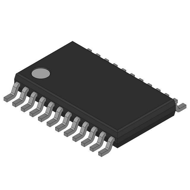
24
SOIC−24
DW SUFFIX
CASE 751E
1
1
Features
•
•
•
•
•
•
•
•
•
LVX4245
AWLYYWWG
Bi−directional Interface Between 5.0 V and 3.0 V Buses
Control Inputs Compatible with TTL Level
5.0 V Data Flow at A Port and 3.0 V Data Flow at B Port
Outputs Source/Sink 24 mA at 5.0 V Bus and 12 mA at 3.0 V Bus
Guaranteed Simultaneous Switching Noise Level and Dynamic
Threshold Performance
Available in SOIC and TSSOP Packages
Functionally Compatible with the 74 Series 245
NLV Prefix for Automotive and Other Applications Requiring
Unique Site and Control Change Requirements; AEC−Q100
Qualified and PPAP Capable
These Devices are Pb−Free, Halogen Free/BFR Free and are RoHS
Compliant
24
24
LVX
4245G
ALYW
TSSOP−24
DT SUFFIX
CASE 948H
1
1
LVX4245
A
WL, L
Y
WW, W
G or G
= Specific Device Code
= Assembly Location
= Wafer Lot
= Year
= Work Week
= Pb−Free Package
(Note: Microdot may be in either location)
PIN NAMES
VCCB VCCB OE
24
23
22
B0
B1
B2
B3
B4
B5
B6
B7
GND
21
20
19
18
17
16
15
14
13
Pins
Function
OE
T/R
A0−A7
Output Enable Input
Transmit/Receive Input
Side A 3−State Inputs or 3−State
Outputs
Side B 3−State Inputs or 3−State
Outputs
B0−B7
1
2
VCCA T/R
3
4
5
6
7
8
9
10
A0
A1
A2
A3
A4
A5
A6
A7
11
12
ORDERING INFORMATION
GND GND
See detailed ordering and shipping information in the package
dimensions section on page 5 of this data sheet.
Figure 1. 24−Lead Pinout
(Top View)
© Semiconductor Components Industries, LLC, 2011
July, 2017 − Rev. 6
1
Publication Order Number:
MC74LVX4245/D
�MC74LVX4245
OE 22
T/R 2
A0
3
21
A1
B0
4
20
A2
B1
5
19
A3
B2
6
18
A4
B3
7
17
A5
B4
8
16
A6
B5
9
15
A7
B6
10
14
B7
Figure 2. Logic Diagram
INPUTS
OE
T/R
OPERATING MODE
Non−Inverting
L
L
B Data to A Bus
L
H
A Data to B Bus
H
X
Z
H = High Voltage Level; L = Low Voltage Level; Z = High Impedance State; X = High or Low Voltage Level
and Transitions are Acceptable; For ICC reasons, Do Not Float Inputs
www.onsemi.com
2
�MC74LVX4245
ABSOLUTE MAXIMUM RATINGS
Symbol
VCCA,
VCCB
VI
VI/O
Parameter
DC Supply Voltage
DC Input Voltage
Condition
Unit
−0.5 to +7.0
V
OE, T/R
−0.5 to VCCA +0.5
V
An
−0.5 to VCCA +0.5
V
Bn
−0.5 to VCCB +0.5
V
DC Input/Output Voltage
±20
VI < GND
mA
DC Output Diode Current
±50
VO < GND; VO > VCC
mA
DC Output Source/Sink Current
±50
mA
±50
±200
±100
mA
−65 to +150
°C
±300
mA
IIK
DC Input Diode Current
IOK
IO
OE, T/R
ICC,
IGND
DC Supply Current
TSTG
Storage Temperature Range
Latchup
Value
Per Output Pin
Maximum Current at ICCA
Maximum Current at ICCB
DC Latchup Source/Sink Current
Stresses exceeding those listed in the Maximum Ratings table may damage the device. If any of these limits are exceeded, device functionality
should not be assumed, damage may occur and reliability may be affected.
RECOMMENDED OPERATING CONDITIONS
Symbol
VCCA,
VCCB
VI
VI/O
TA
Dt/DV
Parameter
Min
Max
Unit
4.5
2.7
5.5
3.6
V
OE, T/R
0
VCCA
V
An
Bn
0
0
VCCA
VCCB
V
−40
+85
°C
0
8
ns/V
Supply Voltage
VCCA
VCCB
Input Voltage
Input/Output Voltage
Operating Free−Air Temperature
Minimum Input Edge Rate
VIN from 30% to 70% of VCC; VCC at 3.0V, 4.5V, 5.5V
Functional operation above the stresses listed in the Recommended Operating Ranges is not implied. Extended exposure to stresses beyond
the Recommended Operating Ranges limits may affect device reliability.
DC ELECTRICAL CHARACTERISTICS
TA = 25°C
Symbol
VIHA
VIHB
VILA
VILB
VOHA
VOHB
VOLA
VOLB
Parameter
Minimum HIGH
Level
Input Voltage
Condition
An,OE
T/R
Bn
Maximum LOW
Level
Input Voltage
An,OE
T/R
Bn
VOUT ≤ 0.1V
or
≥ VCC − 0.1V
VOUT ≤ 0.1V
or
≥ VCC − 0.1V
Typ
TA = −40 to +85°C
VCCA
VCCB
Guaranteed Limits
Unit
5.5
4.5
3.3
3.3
2.0
2.0
2.0
2.0
V
5.0
5.0
3.6
2.7
2.0
2.0
2.0
2.0
V
5.5
4.5
3.3
3.3
0.8
0.8
0.8
0.8
V
5.0
5.0
2.7
3.6
0.8
0.8
0.8
0.8
V
Minimum HIGH
Level
Output Voltage
IOUT = −100mA
IOH = −24mA
4.5
4.5
3.0
3.0
4.50
4.25
4.40
3.86
4.40
3.76
V
IOUT = −100mA
IOH = −12mA
IOH = −8mA
4.5
4.5
4.5
3.0
3.0
2.7
2.99
2.80
2.50
2.9
2.4
2.4
2.9
2.4
2.4
V
Maximum LOW
Level
Output Voltage
IOUT = 100mA
IOL = 24mA
4.5
4.5
3.0
3.0
0.002
0.18
0.10
0.36
0.10
0.44
V
IOUT = 100mA
IOL = 12mA
IOL = 8mA
4.5
4.5
4.5
3.0
3.0
2.7
0.002
0.1
0.1
0.10
0.31
0.31
0.10
0.40
0.40
V
www.onsemi.com
3
�MC74LVX4245
DC ELECTRICAL CHARACTERISTICS
TA = 25°C
Symbol
IIN
IOZA
IOZB
Parameter
Condition
VCCA
VCCB
OE,
T/R
VI = VCCA, GND
5.5
3.6
±0.1
±1.0
Max 3−State Output Leakage
An
VI = VIH, VIL
OE = VCCA
VO = VCCA, GND
5.5
3.6
±0.5
±5.0
Max 3−State Output Leakage
Bn
VI = VIH, VIL
OE = VCCA
VO = VCCB, GND
5.5
3.6
±0.5
±5.0
VI=VCCA−2.1V
5.5
3.6
1.35
1.5
VI=VCCB−0.6V
5.5
3.6
0.35
0.5
Max Input Leakage
Current
Typ
Guaranteed Limits
DICC
Maximum ICCT
per Input
ICCA
Quiescent VCCA
Supply Current
An=VCCA or GND
Bn=VCCB or GND
OE=GND
T/R=GND
Quiescent VCCB
Supply Current
An=VCCA or GND
Bn=VCCB or GND
OE=GND
T/R=VCCA
5.5
3.6
5
An,OE
T/R
Bn
ICCB
TA = −40 to +85°C
1.0
Unit
mA
mA
mA
mA
mA
mA
5.5
3.6
8
80
mA
50
VOLPA
VOLPB
Quiet Output Max
Dynamic VOL
Notes 1, 2
5.0
5.0
3.3
3.3
1.5
1.2
V
VOLVA
VOLVB
Quiet Output Min
Dynamic VOL
Notes 1, 2
5.0
5.0
3.3
3.3
−1.2
−0.8
V
VIHDA
VIHDB
Min HIGH Level
Dynamic Input
Voltage
Notes 1, 3
5.0
5.0
3.3
3.3
2.0
2.0
VILDA
VILDB
Max LOW Level
Dynamic Input
Voltage
Notes 1, 3
5.0
5.0
3.3
3.3
0.8
0.8
V
V
Product parametric performance is indicated in the Electrical Characteristics for the listed test conditions, unless otherwise noted. Product
performance may not be indicated by the Electrical Characteristics if operated under different conditions.
1. Worst case package.
2. Max number of outputs defined as (n). Data inputs are driven 0V to VCC level; one output at GND.
3. Max number of data inputs (n) switching. (n−1) inputs switching 0V to VCC level. Input under test switching: VCC level to threshold (VIHD),
0V to threshold (VILD), f = 1MHz.
CAPACITIVE CHARACTERISTICS
Symbol
Parameter
Condition
Typical
Unit
CIN
Input Capacitance
VCCA = 5.0V; VCCB = 3.3V
4.5
pF
CI/O
Input/Output Capacitance
VCCA = 5.0V; VCCB = 3.3V
15
pF
CPD
Power Dissipation Capacitance
(Measured at 10MHz)
VCCA = 5.0V
VCCB = 3.3V
55
40
pF
B→A
A→B
www.onsemi.com
4
�MC74LVX4245
AC ELECTRICAL CHARACTERISTICS
Symbol
Parameter
TA = −40 to +85°C
CL = 50pF
TA = −40 to +85°C
CL = 50pF
VCCA = 5V ±0.5V
VCCB = 3.3V ±0.3V
VCCA = 5V ±0.5V
VCCB = 2.7V
Min
Typ
(Note 4)
Max
Min
Max
Unit
tPHL
tPLH
Propagation Delay A to B
1.0
1.0
5.1
5.3
9.0
9.0
1.0
1.0
10.0
10.0
ns
tPHL
tPLH
Propagation Delay B to A
1.0
1.0
5.4
5.5
9.0
9.0
1.0
1.0
10.0
10.0
ns
tPZL
tPZH
Output Enable Time OE to B
1.0
1.0
6.5
6.7
10.5
10.5
1.0
1.0
11.5
11.5
ns
tPZL
tPZH
Output Enable Time OE to A
1.0
1.0
5.2
5.8
9.5
9.5
1.0
1.0
10.0
10.0
ns
tPHZ
tPLZ
Output Disable Time OE to B
1.0
1.0
6.0
3.3
10.0
7.0
1.0
1.0
10.0
7.5
ns
tPHZ
tPLZ
Output Disable Time OE to A
1.0
1.0
3.9
2.9
7.5
7.0
1.0
1.0
7.5
7.5
ns
1.0
1.5
tOSHL
tOSLH
Output to Output Skew, Data to Output (Note 5)
1.5
ns
4. Typical values at VCCA = 5.0V; VCCB = 3.3V at 25°C.
5. Skew is defined as the absolute value of the difference between the actual propagation delay for any two separate outputs of the same device.
The specification applies to any outputs switching in the same direction, either HIGH−to−LOW (tOSHL) or LOW−to−HIGH (tOSLH); parameter
guaranteed by design.
ORDERING INFORMATION
Device
MC74LVX4245DWG
MC74LVX4245DWR2G
Package
Shipping†
SOIC−24
(Pb−Free)
30 Units / Rail
MC74LVX4245DTG
MC74LVX4245DTR2G
1000 / Tape & Reel
62 Units / Rail
TSSOP−24
(Pb−Free)
NLVLVX4245DTR2G*
2500 / Tape & Reel
2500 / Tape & Reel
†For information on tape and reel specifications, including part orientation and tape sizes, please refer to our Tape and Reel Packaging
Specifications Brochure, BRD8011/D.
*NLV Prefix for Automotive and Other Applications Requiring Unique Site and Control Change Requirements; AEC−Q100 Qualified and PPAP
Capable.
www.onsemi.com
5
�MC74LVX4245
Dual Supply Octal Translating Transceiver
The 74LVX4245 is a is a dual−supply device well capable
of bidirectional signal voltage translation. This level shifting
ability provides an excellent interface between low voltage
CPU local bus and a standard 5.0 V I/O bus. The device
control inputs can be controlled by either the low voltage
CPU and core logic or a bus arbitrator with 5.0 V I/O levels.
The LVX4245 is ideal for mixed voltage applications such
as notebook computers using a 3.3 V CPU and 5.0 V
peripheral devices.
LOW VOLTAGE CPU LOCAL BUS
VCCB
VCCB
LVX4245
VCCA
Applications:
Mixed Mode Dual Supply Interface Solutions
LVX4245
VCCA
EISA - ISA - MCA
(5V I/O LEVELS)
The LVX4245 is designed to solve 3.0 V / 5.0 V interfaces
when CMOS devices cannot tolerate I/O levels above their
applied VCC. If an I/O pin of a 3.0 V device is driven by a 5.0
V device, the P−Channel transistor in the 3.0 V device will
conduct − causing current flow from the I/O bus to the 3.0 V
power supply. The result may be destruction of the 3.0 V
device through latchup effects. A current limiting resistor
may be used to prevent destruction, but it causes speed
degradation and needless power dissipation.
A better solution is provided in the LVX4245. It provides
two different output levels that easily handle the dual voltage
interface. The A port is a dedicated 5.0 V port; the B port is
a dedicated 3.0 V port.
Since the LVX4245 is a ‘245 transceiver, the user may
either use it for bidirectional or unidirectional applications.
The center 20 pins are configured to match a ‘245 pinout.
This enables the user to easily replace this level shifter with
a 3.0 V ‘245 device without additional layout work or re−
manufacture of the circuit board (when both buses are 3.0 V).
Figure 3. 3.3V/5V Interface Block Diagram
Powering Up the LVX4245
When powering up the LVX4245, please note that if the
VCCB pin is powered−up well in advance of the VCCA pin,
several milliamps of either ICCA or ICCB current will result.
If the VCCA pin is powered−up in advance of the VCCB pin
then only nanoamps of Icc current will result. In actuality the
VCCB can be powered “slightly” before the VCCA without
the current penalty, but this “setup time” is dependent on the
power−up ramp rate of the VCC pins. With a ramp rate of
approximately 50 mV/ns (50V/ms) a 25 ns setup time was
observed (VCCB before VCCA). With a 7.0 V/ms rate, the
setup time was about 140ns. When all is said and done, the
safest powerup strategy is to simply power VCCA before
VCCB. One more note: if the VCCB ramp rate is faster than
the VCCA ramp rate then power problems might still occur,
even if the VCCA powerup began prior to the VCCB powerup.
www.onsemi.com
6
�MC74LVX4245
5V
MICROCHANNEL/
EISA/ISA/AT
5V BUS
LOCAL
3V BUS
KEYBOARD
CONTROLLER
3V
CACHE
SRAM
SUPER
I/O
5V
VCCA
3V
VCCB
CPU
386/486
CORE
LOGIC
LVX4245
TRANSCEIVERS
A PORT
A0:7
B PORT
B0:7
ROM
BIOS
PCMCIA
CONTROLLER
MEMORY
DRIVER
VGA
CONTROLLER
Figure 4. MC74LVX4245 Fits Into a System with 3V Subsystem and 5V Subsystem
VCCA
MC74LVX4245
(T/R) DIR
VCCB
VCCB
A0
OE
A1
B0
A2
A3
A4
STANDARD
74 SERIES
`245
B1
B2
B3
A5
B4
A6
B5
A7
B6
GND
B7
GND
GND
Figure 5. MC74LVX4245 Pin Arrangement Is Compatible to 20−Pin 74 Series ‘245s
www.onsemi.com
7
�MC74LVX4245
VCC
An, Bn
50% VCC
50% VCC
0V
tPLH
tPHL
VOH
50% VCC
Bn, An
50% VCC
VOL
WAVEFORM 1 - PROPAGATION DELAYS
tR = tF = 2.5ns, 10% to 90%; f = 1MHz; tW = 500ns
VCCA
50% VCC
50% VCC
OE, T/R
0V
tPZH
tPHZ
VCC
VOH - 0.3V
50% VCC
An, Bn
≈ 0V
tPZL
tPLZ
≈ VCC
50% VCC
An, Bn
VOL + 0.3V
GND
WAVEFORM 2 - OUTPUT ENABLE AND DISABLE TIMES
tR = tF = 2.5ns, 10% to 90%; f = 1MHz; tW = 500ns
Figure 6. AC Waveforms
VCC
R1
PULSE
GENERATOR
DUT
RT
CL
TEST
RL
SWITCH
tPLH, tPHL, tPZH, tPHZ
Open
2 × VCC
tPZL, tPLZ
CL = 50pF or equivalent (Includes jig and probe capacitance)
RL = R1 = 500W or equivalent
RT = ZOUT of pulse generator (typically 50W)
Figure 7. Test Circuit
www.onsemi.com
8
2 × VCC
OPEN
�MC74LVX4245
PACKAGE DIMENSIONS
SOIC−24
DW SUFFIX
CASE 751E−04
ISSUE F
D
A
B
0.25 C
24
E
NOTES:
1. DIMENSIONING AND TOLERANCING PER ASME
Y14.5M, 1994.
2. CONTROLLING DIMENSION: MILLIMETERS.
3. DIMENSIONS b AND c APPLY TO THE FLAT SECTION OF THE LEAD AND ARE MEASURED BETWEEN 0.10 AND 0.25 FROM THE LEAD TIP.
4. DIMENSIONS D AND E1 DO NOT INCLUDE MOLD
FLASH, PROTRUSIONS OR GATE BURRS. MOLD
FLASH, PROTRUSIONS OR GATE BURRS SHALL
NOT EXCEED 0.15 mm PER SIDE. INTERLEAD
FLASH OR PROTRUSION SHALL NOT EXCEED
0.25 PER SIDE. DIMENSIONS D AND E1 ARE
DETERMINED AT DATUM H.
5. A1 IS DEFINED AS THE VERTICAL DISTANCE
FROM THE SEATING PLANE TO THE LOWEST
POINT ON THE PACKAGE BODY.
H
13
E1
1
L
12
C
DETAIL A
24X b
PIN 1
INDICATOR
0.25
TOP VIEW
M
C A
S
B
S
h
x 45 _
A
A1
e
NOTE 5
DIM
A
A1
b
c
D
E
E1
e
h
L
M
NOTE 3
C
M
c
SEATING
PLANE
NOTE 3
DETAIL A
END VIEW
SIDE VIEW
MILLIMETERS
MIN
MAX
2.35
2.65
0.13
0.29
0.35
0.49
0.23
0.32
15.25
15.54
10.30 BSC
7.40
7.60
1.27 BSC
0.25
0.75
0.41
0.90
0_
8_
RECOMMENDED
SOLDERING FOOTPRINT*
24X
24X
1.62
0.52
11.00
1
1.27
PITCH
DIMENSIONS: MILLIMETERS
*For additional information on our Pb−Free strategy and soldering
details, please download the ON Semiconductor Soldering and
Mounting Techniques Reference Manual, SOLDERRM/D.
www.onsemi.com
9
�MC74LVX4245
PACKAGE DIMENSIONS
TSSOP−24
DT SUFFIX
CASE 948H
ISSUE B
NOTE 4
B
NOTE 5
A
D
NOTE 6
NOTE 6
24
L2
13
GAUGE
PLANE
E1
L
E
C
DETAIL A
PIN 1
1
REFERENCE
12
e
24X
TOP VIEW
0.15 C B
b
0.10
C B
M
S
A
H
A1
0.10 C
24X
SIDE VIEW
S
NOTE 3
A
0.05 C
S
2X 12 TIPS
NOTES:
1. DIMENSIONING AND TOLERANCING PER ASME Y14.5M, 1994.
2. CONTROLLING DIMENSION: MILLIMETERS.
3. DIMENSION b DOES NOT INCLUDE DAMBAR PROTRUSION.
DAMBAR PROTRUSION SHALL BE 0.08 MAX AT MMC. DAMBAR
CANNOT BE LOCATED ON THE LOWER RADIUS OF THE FOOT.
4. DIMENSION D DOES NOT INCLUDE MOLD FLASH,
PROTRUSIONS OR GATE BURRS. MOLD FLASH, PROTRUSIONS
OR GATE BURRS SHALL NOT EXCEED 0.15 PER SIDE. DIMENSION D IS DETERMINED AT DATUM PLANE H.
5. DIMENSION E1 DOES NOT INCLUDE INTERLEAD FLASH OR
PROTRUSION. INTERLEAD FLASH OR PROTRUSION SHALL NOT
EXCEED 0.25 PER SIDE. DIMENSION E1 IS DETERMINED AT DATUM PLANE H.
6. DATUMS A AND B ARE DETERMINED AT DATUM PLANE H.
7. A1 IS DEFINED AS THE VERTICAL DISTANCE FROM THE SEATING PLANE TO THE LOWEST POINT ON THE PACKAGE BODY.
C
SEATING
PLANE
DETAIL A
c
END VIEW
M
DIM
A
A1
b
c
D
E
E1
e
L
L2
M
MILLIMETERS
MIN
MAX
1.20
--0.05
0.15
0.19
0.30
0.09
0.20
7.90
7.70
6.40 BSC
4.30
4.50
0.65 BSC
0.50
0.75
0.25 BSC
0_
8_
RECOMMENDED
SOLDERING FOOTPRINT
24X
0.42
24X
1.15
6.70
0.65
PITCH
DIMENSIONS: MILLIMETERS
ON Semiconductor and
are trademarks of Semiconductor Components Industries, LLC dba ON Semiconductor or its subsidiaries in the United States and/or other countries.
ON Semiconductor owns the rights to a number of patents, trademarks, copyrights, trade secrets, and other intellectual property. A listing of ON Semiconductor’s product/patent
coverage may be accessed at www.onsemi.com/site/pdf/Patent−Marking.pdf. ON Semiconductor reserves the right to make changes without further notice to any products herein.
ON Semiconductor makes no warranty, representation or guarantee regarding the suitability of its products for any particular purpose, nor does ON Semiconductor assume any liability
arising out of the application or use of any product or circuit, and specifically disclaims any and all liability, including without limitation special, consequential or incidental damages.
Buyer is responsible for its products and applications using ON Semiconductor products, including compliance with all laws, regulations and safety requirements or standards,
regardless of any support or applications information provided by ON Semiconductor. “Typical” parameters which may be provided in ON Semiconductor data sheets and/or
specifications can and do vary in different applications and actual performance may vary over time. All operating parameters, including “Typicals” must be validated for each customer
application by customer’s technical experts. ON Semiconductor does not convey any license under its patent rights nor the rights of others. ON Semiconductor products are not
designed, intended, or authorized for use as a critical component in life support systems or any FDA Class 3 medical devices or medical devices with a same or similar classification
in a foreign jurisdiction or any devices intended for implantation in the human body. Should Buyer purchase or use ON Semiconductor products for any such unintended or unauthorized
application, Buyer shall indemnify and hold ON Semiconductor and its officers, employees, subsidiaries, affiliates, and distributors harmless against all claims, costs, damages, and
expenses, and reasonable attorney fees arising out of, directly or indirectly, any claim of personal injury or death associated with such unintended or unauthorized use, even if such
claim alleges that ON Semiconductor was negligent regarding the design or manufacture of the part. ON Semiconductor is an Equal Opportunity/Affirmative Action Employer. This
literature is subject to all applicable copyright laws and is not for resale in any manner.
PUBLICATION ORDERING INFORMATION
LITERATURE FULFILLMENT:
Literature Distribution Center for ON Semiconductor
19521 E. 32nd Pkwy, Aurora, Colorado 80011 USA
Phone: 303−675−2175 or 800−344−3860 Toll Free USA/Canada
Fax: 303−675−2176 or 800−344−3867 Toll Free USA/Canada
Email: orderlit@onsemi.com
◊
N. American Technical Support: 800−282−9855 Toll Free
USA/Canada
Europe, Middle East and Africa Technical Support:
Phone: 421 33 790 2910
Japan Customer Focus Center
Phone: 81−3−5817−1050
www.onsemi.com
10
ON Semiconductor Website: www.onsemi.com
Order Literature: http://www.onsemi.com/orderlit
For additional information, please contact your local
Sales Representative
MC74LVX4245/D
�