MMBD352LT1G, MMBD353LT1G, MMBD354LT1G, MMBD355LT1G Dual Hot Carrier Mixer Diodes
These devices are designed primarily for UHF mixer applications but are suitable also for use in detector and ultra−fast switching circuits.
Features
1 2
http://onsemi.com
3
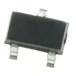
SOT−23 (TO−236) CASE 318
• Very Low Capacitance − Less Than 1.0 pF @ Zero V • Low Forward Voltage − 0.5 V (Typ) @ IF = 10 mA • These Devices are Pb−Free, Halogen Free/BFR Free and are RoHS
Compliant
MAXIMUM RATINGS (EACH DIODE)
Rating Continuous Reverse Voltage Symbol VR Value 7.0 Unit VCC
1 ANODE
3 CATHODE/ANODE MMBD352LT1 STYLE 11
2 CATHODE
1 CATHODE
THERMAL CHARACTERISTICS
Characteristic Total Device Dissipation FR−5 Board, (Note 1) TA = 25°C Derate above 25°C Thermal Resistance, Junction−to−Ambient Total Device Dissipation Alumina Substrate, (Note 2) TA = 25°C Derate above 25°C Thermal Resistance, Junction−to−Ambient Junction and Storage Temperature Symbol PD Max 225 1.8 556 300 2.4 417 −55 to +150 Unit mW mW/°C °C/W mW mW/°C °C/W °C ANODE 3
3 CATHODE/ANODE MMBD353LT1 STYLE 19
2 ANODE
RqJA PD
3 CATHODE MMBD354LT1 STYLE 9
1 ANODE 2 ANODE
RqJA TJ, Tstg
1 CATHODE 2 CATHODE MMBD355LT1 STYLE 12
Maximum ratings are those values beyond which device damage can occur. Maximum ratings applied to the device are individual stress limit values (not normal operating conditions) and are not valid simultaneously. If these limits are exceeded, device functional operation is not implied, damage may occur and reliability may be affected. 1. FR−5 = 1.0 x 0.75 x 0.062 in. 2. Alumina = 0.4 x 0.3 x 0.024 in. 99.5% alumina.
MARKING DIAGRAM
(EACH DIODE)
ELECTRICAL CHARACTERISTICS (TA = 25°C unless otherwise noted)
Rating Forward Voltage (IF = 10 mAdc) Reverse Leakage Current (Note 3) (VR = 3.0 V) (VR = 7.0 V) Capacitance (VR = 0 V, f = 1.0 MHz) Symbol VF IR Min − Max 0.60 Unit V mA 1
Mxx M G G Mxx = Device Code M = Date Code* G = Pb−Free Package (Note: Microdot may be in either location) *Date Code orientation and/or overbar may vary depending upon manufacturing location.
− − −
0.25 10 1.0
C
pF
ORDERING INFORMATION
See detailed ordering, marking, and shipping information in the package dimensions section on page 2 of this data sheet.
3. For each individual diode while the second diode is unbiased.
© Semiconductor Components Industries, LLC, 2009
August, 2009 − Rev. 7
1
Publication Order Number: MMBD352LT1/D
�MMBD352LT1G, MMBD353LT1G, MMBD354LT1G, MMBD355LT1G
TYPICAL CHARACTERISTICS
100 I F, FORWARD CURRENT (mA) 1.0
10 TA = -40°C
C, CAPACITANCE (pF) 0.8
TA = 85°C
0.9
0.8
1.0
TA = 25°C
0.7
0.1 0.3 0.4 0.5 0.6 0.7 VF, FORWARD VOLTAGE (VOLTS)
0.6 0 1.0 2.0 3.0 4.0 VR, REVERSE VOLTAGE (VOLTS)
Figure 1. Forward Voltage
Figure 2. Capacitance
ORDERING INFORMATION
Device MMBD352LT1G MMBD352LT3G MMBD353LT1G MMBD353LT3G MMBD354LT1G MMBD355LT1G M4F M5G Marking Package SOT−23 (Pb−Free) SOT−23 (Pb−Free) SOT−23 (Pb−Free) SOT−23 (Pb−Free) SOT−23 (Pb−Free) SOT−23 (Pb−Free) Shipping† 3,000 Units / Tape & Reel 10,000 Units / Tape & Reel 3,000 Units / Tape & Reel 10,000 Units / Tape & Reel 3,000 Units / Tape & Reel 3,000 Units / Tape & Reel
M6H MJ1
†For information on tape and reel specifications, including part orientation and tape sizes, please refer to our Tape and Reel Packaging Specifications Brochure, BRD8011/D.
http://onsemi.com
2
�MMBD352LT1G, MMBD353LT1G, MMBD354LT1G, MMBD355LT1G
PACKAGE DIMENSIONS
SOT−23 (TO−236) CASE 318−08 ISSUE AN
D
SEE VIEW C 3 NOTES: 1. DIMENSIONING AND TOLERANCING PER ANSI Y14.5M, 1982. 2. CONTROLLING DIMENSION: INCH. 3. MAXIMUM LEAD THICKNESS INCLUDES LEAD FINISH THICKNESS. MINIMUM LEAD THICKNESS IS THE MINIMUM THICKNESS OF BASE MATERIAL. 4. 318−01 THRU −07 AND −09 OBSOLETE, NEW STANDARD 318−08.
E
1 2
HE c e b q 0.25
A A1 MMBD352LT1
STYLE 11: PIN 1. ANODE 2. CATHODE 3. CATHODE−ANODE
L L1 VIEW C
DIM A A1 b c D E e L L1 HE
MIN 0.89 0.01 0.37 0.09 2.80 1.20 1.78 0.10 0.35 2.10
MILLIMETERS NOM MAX 1.00 1.11 0.06 0.10 0.44 0.50 0.13 0.18 2.90 3.04 1.30 1.40 1.90 2.04 0.20 0.30 0.54 0.69 2.40 2.64
MIN 0.035 0.001 0.015 0.003 0.110 0.047 0.070 0.004 0.014 0.083
INCHES NOM 0.040 0.002 0.018 0.005 0.114 0.051 0.075 0.008 0.021 0.094
MAX 0.044 0.004 0.020 0.007 0.120 0.055 0.081 0.012 0.029 0.104
MMBD353LT1
STYLE 19: PIN 1. CATHODE 2. ANODE 3. CATHODE−ANODE
SOLDERING FOOTPRINT*
0.95 0.037 0.95 0.037
MMBD354LT1
STYLE 9: PIN 1. ANODE 2. ANODE 3. CATHODE
MMBD355LT1
STYLE 12: PIN 1. CATHODE 2. CATHODE 3. ANODE
2.0 0.079 0.9 0.035
SCALE 10:1
0.8 0.031
mm inches
*For additional information on our Pb−Free strategy and soldering details, please download the ON Semiconductor Soldering and Mounting Techniques Reference Manual, SOLDERRM/D.
ON Semiconductor and are registered trademarks of Semiconductor Components Industries, LLC (SCILLC). SCILLC reserves the right to make changes without further notice to any products herein. SCILLC makes no warranty, representation or guarantee regarding the suitability of its products for any particular purpose, nor does SCILLC assume any liability arising out of the application or use of any product or circuit, and specifically disclaims any and all liability, including without limitation special, consequential or incidental damages. “Typical” parameters which may be provided in SCILLC data sheets and/or specifications can and do vary in different applications and actual performance may vary over time. All operating parameters, including “Typicals” must be validated for each customer application by customer’s technical experts. SCILLC does not convey any license under its patent rights nor the rights of others. SCILLC products are not designed, intended, or authorized for use as components in systems intended for surgical implant into the body, or other applications intended to support or sustain life, or for any other application in which the failure of the SCILLC product could create a situation where personal injury or death may occur. Should Buyer purchase or use SCILLC products for any such unintended or unauthorized application, Buyer shall indemnify and hold SCILLC and its officers, employees, subsidiaries, affiliates, and distributors harmless against all claims, costs, damages, and expenses, and reasonable attorney fees arising out of, directly or indirectly, any claim of personal injury or death associated with such unintended or unauthorized use, even if such claim alleges that SCILLC was negligent regarding the design or manufacture of the part. SCILLC is an Equal Opportunity/Affirmative Action Employer. This literature is subject to all applicable copyright laws and is not for resale in any manner.
PUBLICATION ORDERING INFORMATION
LITERATURE FULFILLMENT: Literature Distribution Center for ON Semiconductor P.O. Box 5163, Denver, Colorado 80217 USA Phone : 303−675−2175 or 800−344−3860 Toll Free USA/Canada Fax: 303−675−2176 or 800−344−3867 Toll Free USA/Canada Email: orderlit@onsemi.com N. American Technical Support: 800−282−9855 Toll Free USA/Canada Europe, Middle East and Africa Technical Support: Phone: 421 33 790 2910 Japan Customer Focus Center Phone: 81−3−5773−3850 ON Semiconductor Website: www.onsemi.com Order Literature: http://www.onsemi.com/orderlit For additional information, please contact your local Sales Representative
http://onsemi.com
3
MMBD352LT1/D
�


 工商网监
湘ICP备2023018690号
工商网监
湘ICP备2023018690号
