Is Now Part of
To learn more about ON Semiconductor, please visit our website at
www.onsemi.com
Please note: As part of the Fairchild Semiconductor integration, some of the Fairchild orderable part numbers
will need to change in order to meet ON Semiconductor’s system requirements. Since the ON Semiconductor
product management systems do not have the ability to manage part nomenclature that utilizes an underscore
(_), the underscore (_) in the Fairchild part numbers will be changed to a dash (-). This document may contain
device numbers with an underscore (_). Please check the ON Semiconductor website to verify the updated
device numbers. The most current and up-to-date ordering information can be found at www.onsemi.com. Please
email any questions regarding the system integration to Fairchild_questions@onsemi.com.
ON Semiconductor and the ON Semiconductor logo are trademarks of Semiconductor Components Industries, LLC dba ON Semiconductor or its subsidiaries in the United States and/or other countries. ON Semiconductor owns the rights to a number
of patents, trademarks, copyrights, trade secrets, and other intellectual property. A listing of ON Semiconductor’s product/patent coverage may be accessed at www.onsemi.com/site/pdf/Patent-Marking.pdf. ON Semiconductor reserves the right
to make changes without further notice to any products herein. ON Semiconductor makes no warranty, representation or guarantee regarding the suitability of its products for any particular purpose, nor does ON Semiconductor assume any liability
arising out of the application or use of any product or circuit, and specifically disclaims any and all liability, including without limitation special, consequential or incidental damages. Buyer is responsible for its products and applications using ON
Semiconductor products, including compliance with all laws, regulations and safety requirements or standards, regardless of any support or applications information provided by ON Semiconductor. “Typical” parameters which may be provided in ON
Semiconductor data sheets and/or specifications can and do vary in different applications and actual performance may vary over time. All operating parameters, including “Typicals” must be validated for each customer application by customer’s
technical experts. ON Semiconductor does not convey any license under its patent rights nor the rights of others. ON Semiconductor products are not designed, intended, or authorized for use as a critical component in life support systems or any FDA
Class 3 medical devices or medical devices with a same or similar classification in a foreign jurisdiction or any devices intended for implantation in the human body. Should Buyer purchase or use ON Semiconductor products for any such unintended
or unauthorized application, Buyer shall indemnify and hold ON Semiconductor and its officers, employees, subsidiaries, affiliates, and distributors harmless against all claims, costs, damages, and expenses, and reasonable attorney fees arising out
of, directly or indirectly, any claim of personal injury or death associated with such unintended or unauthorized use, even if such claim alleges that ON Semiconductor was negligent regarding the design or manufacture of the part. ON Semiconductor
is an Equal Opportunity/Affirmative Action Employer. This literature is subject to all applicable copyright laws and is not for resale in any manner.
�MMBF4091/MMBF4092/MMBF4093
N-Channel Switch
Features
• This device is designed for low level analog switching applications, sample and hold circuits and chopper stabilized
amplifiers.
• Sourced from Process 51.
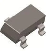
G
D
SOT-23
S
Mark: 61J / 61K / 61L
NOTE: Source & Drain
are interchangeable
Ordering Information
Part Number
Top Mark
Package
Packing Method
MMBF4091
61J
SOT 23
Tape and Reel
MMBF4092
61K
SOT 23
Tape and Reel
MMBF4093
61L
SOT 23
Tape and Reel
Absolute Maximum Ratings(1), (2)
Stresses exceeding the absolute maximum ratings may damage the device. The device may not function or be operable above the recommended operating conditions and stressing the parts to these levels is not recommended. In addition, extended exposure to stresses above the recommended operating conditions may affect device reliability. The
absolute maximum ratings are stress ratings only. Values are at TA = 25°C unless otherwise noted.
Symbol
Parameter
Value
Unit
V
VDG
Drain-Gate Voltage
40
VGS
Gate-Source Voltage
-40
V
IGF
Forward Gate Current
50
mA
-55 to 150
C
TJ, TSTG
Operating and Storage Junction Temperature Range
Notes:
1. These ratings are based on a maximum junction temperature of 150C.
2. These are steady-state limits. Fairchild Semiconductor should be consulted on applications involving pulsed or
low-duty-cycle operations.
© 2000 Fairchild Semiconductor Corporation
MMBF4091/MMBF4092/MMBF4093 Rev. 1.3
www.fairchildsemi.com
MMBF4091/MMBF4092/MMBF4093 — N-Channel Switch
July 2016
�Values are at TA = 25°C unless otherwise noted.
Symbol
PD
RJA
Parameter
Max.
Unit
Total Device Dissipation
350
mW
Derate Above 25C
2.8
mW/C
Thermal Resistance, Junction-to-Ambient(3)
357
C/W
Notes:
3. Device mounted on FR-4 PCB, 1.6” x 1.6” x 0.06”.
Electrical Characteristics
Values are at TA = 25°C unless otherwise noted.
Symbol
Parameter
Conditions
Min.
Max.
Unit
Off Characteristics
V(BR)GSS Gate-Source Breakdown Voltage
IG = 1 A, VDS = 0
VGS(off)
VDS = 20 V, ID = 1 nA
Gate-Source Cut-Off Voltage
-40
MMBF4091
MMBF4092
MMBF4093
-5.0
-2.0
-1.0
V
-10.0
-7.0
-5.0
V
IDGO
Drain-Gate Leakage Current
VDS = 20 V, Is = 0
VDS = 20 V, Is = 0, TA = 150°C
-200
-400
pA
nA
ID(off)
Drain Cutoff Leakage Current
VDS = 20 V, VGS = - 12 V MMBF4091
MMBF4092
VDS = 20 V, VGS = - 8 V
MMBF4093
VDS = 20 V, VGS = - 6 V
VDS = 20 V, VGS = - 12 V,
MMBF4091
TA = 150°C
VDS = 20 V, VGS = - 8 V,
MMBF4092
TA = 150°C
VDS = 20 V, VGS = - 6 V,
MMBF4093
TA = 150°C
200
200
200
pA
pA
pA
400
nA
400
nA
400
nA
On Characteristics
IDSS
Zero-Gate Voltage Drain Current(4) VDS = 20 V, IGS = 0
MMBF4091
MMBF4092
MMBF4093
30
15
8
mA
ID = 6.6 mA, VGS = 0
ID = 4.0 mA, VGS = 0
ID = 2.5 mA, VGS = 0
MMBF4091
MMBF4092
MMBF4093
0.2
0.2
0.2
V
ID = 1 mA, VGS = 0
MMBF4091
MMBF4092
MMBF4093
30
50
80
Drain-Source On Resistance
VDS = VGS = 0, f = 1 kHz
MMBF4091
MMBF4092
MMBF4093
30
50
80
Ciss
Input Capacitance
VDS = 20 V, VGS = 0 V, f = 1.0 MHz
16
pF
Crss
Reverse Transfer Capacitance
VDS = -20 V, f = 1.0 MHz
5
pF
VDS(on)
rDS(on)
Drain-Source On Voltage
Drain-Source On Resistance
Small Signal Characteristics
rDS(on)
© 2000 Fairchild Semiconductor Corporation
MMBF4091/MMBF4092/MMBF4093 Rev. 1.3
www.fairchildsemi.com
2
MMBF4091/MMBF4092/MMBF4093 — N-Channel Switch
Thermal Characteristics
�Parameter
Conditions
Min.
Max.
Unit
Switching Characteristics
tOn
tOff
Turn-On Time
ID(on) = 12 mA
ID(on) = 6.0 mA
ID(on) = 3.0 mA
MMBF4091
MMBF4092
MMBF4093
25
35
60
ns
ns
ns
Turn-Off Time
VGS(off) = 12 V
VGS(off) = 6.0 V
VGS(off) = 3.0 V
MMBF4091
MMBF4092
MMBF4093
40
60
80
ns
ns
ns
Note:
4. Pulse test: pulse width 300 s, duty cycle 1%.
© 2000 Fairchild Semiconductor Corporation
MMBF4091/MMBF4092/MMBF4093 Rev. 1.3
www.fairchildsemi.com
3
MMBF4091/MMBF4092/MMBF4093 — N-Channel Switch
Symbol
��ON Semiconductor and
are trademarks of Semiconductor Components Industries, LLC dba ON Semiconductor or its subsidiaries in the United States and/or other countries.
ON Semiconductor owns the rights to a number of patents, trademarks, copyrights, trade secrets, and other intellectual property. A listing of ON Semiconductor’s product/patent
coverage may be accessed at www.onsemi.com/site/pdf/Patent−Marking.pdf. ON Semiconductor reserves the right to make changes without further notice to any products herein.
ON Semiconductor makes no warranty, representation or guarantee regarding the suitability of its products for any particular purpose, nor does ON Semiconductor assume any liability
arising out of the application or use of any product or circuit, and specifically disclaims any and all liability, including without limitation special, consequential or incidental damages.
Buyer is responsible for its products and applications using ON Semiconductor products, including compliance with all laws, regulations and safety requirements or standards,
regardless of any support or applications information provided by ON Semiconductor. “Typical” parameters which may be provided in ON Semiconductor data sheets and/or
specifications can and do vary in different applications and actual performance may vary over time. All operating parameters, including “Typicals” must be validated for each customer
application by customer’s technical experts. ON Semiconductor does not convey any license under its patent rights nor the rights of others. ON Semiconductor products are not
designed, intended, or authorized for use as a critical component in life support systems or any FDA Class 3 medical devices or medical devices with a same or similar classification
in a foreign jurisdiction or any devices intended for implantation in the human body. Should Buyer purchase or use ON Semiconductor products for any such unintended or unauthorized
application, Buyer shall indemnify and hold ON Semiconductor and its officers, employees, subsidiaries, affiliates, and distributors harmless against all claims, costs, damages, and
expenses, and reasonable attorney fees arising out of, directly or indirectly, any claim of personal injury or death associated with such unintended or unauthorized use, even if such
claim alleges that ON Semiconductor was negligent regarding the design or manufacture of the part. ON Semiconductor is an Equal Opportunity/Affirmative Action Employer. This
literature is subject to all applicable copyright laws and is not for resale in any manner.
PUBLICATION ORDERING INFORMATION
LITERATURE FULFILLMENT:
Literature Distribution Center for ON Semiconductor
19521 E. 32nd Pkwy, Aurora, Colorado 80011 USA
Phone: 303−675−2175 or 800−344−3860 Toll Free USA/Canada
Fax: 303−675−2176 or 800−344−3867 Toll Free USA/Canada
Email: orderlit@onsemi.com
© Semiconductor Components Industries, LLC
N. American Technical Support: 800−282−9855 Toll Free
USA/Canada
Europe, Middle East and Africa Technical Support:
Phone: 421 33 790 2910
Japan Customer Focus Center
Phone: 81−3−5817−1050
www.onsemi.com
1
ON Semiconductor Website: www.onsemi.com
Order Literature: http://www.onsemi.com/orderlit
For additional information, please contact your local
Sales Representative
www.onsemi.com
�


 工商网监
湘ICP备2023018690号
工商网监
湘ICP备2023018690号
