ON Semiconductor
Is Now
To learn more about onsemi™, please visit our website at
www.onsemi.com
onsemi and and other names, marks, and brands are registered and/or common law trademarks of Semiconductor Components Industries, LLC dba “onsemi” or its affiliates and/or
subsidiaries in the United States and/or other countries. onsemi owns the rights to a number of patents, trademarks, copyrights, trade secrets, and other intellectual property. A listing of onsemi
product/patent coverage may be accessed at www.onsemi.com/site/pdf/Patent-Marking.pdf. onsemi reserves the right to make changes at any time to any products or information herein, without
notice. The information herein is provided “as-is” and onsemi makes no warranty, representation or guarantee regarding the accuracy of the information, product features, availability, functionality,
or suitability of its products for any particular purpose, nor does onsemi assume any liability arising out of the application or use of any product or circuit, and specifically disclaims any and all
liability, including without limitation special, consequential or incidental damages. Buyer is responsible for its products and applications using onsemi products, including compliance with all laws,
regulations and safety requirements or standards, regardless of any support or applications information provided by onsemi. “Typical” parameters which may be provided in onsemi data sheets and/
or specifications can and do vary in different applications and actual performance may vary over time. All operating parameters, including “Typicals” must be validated for each customer application
by customer’s technical experts. onsemi does not convey any license under any of its intellectual property rights nor the rights of others. onsemi products are not designed, intended, or authorized
for use as a critical component in life support systems or any FDA Class 3 medical devices or medical devices with a same or similar classification in a foreign jurisdiction or any devices intended for
implantation in the human body. Should Buyer purchase or use onsemi products for any such unintended or unauthorized application, Buyer shall indemnify and hold onsemi and its officers, employees,
subsidiaries, affiliates, and distributors harmless against all claims, costs, damages, and expenses, and reasonable attorney fees arising out of, directly or indirectly, any claim of personal injury or death
associated with such unintended or unauthorized use, even if such claim alleges that onsemi was negligent regarding the design or manufacture of the part. onsemi is an Equal Opportunity/Affirmative
Action Employer. This literature is subject to all applicable copyright laws and is not for resale in any manner. Other names and brands may be claimed as the property of others.
�MT9V034
1/3‐Inch Wide‐VGA CMOS
Digital Image Sensor
General Description
The MT9V034 is a 1/3-inch wide-VGA format CMOS active-pixel
digital image sensor with global shutter and high dynamic range
(HDR) operation. The sensor has specifically been designed to support
the demanding interior and exterior surveillance imaging needs, which
makes this part ideal for a wide variety of imaging applications in
real-world environments.
This wide-VGA CMOS image sensor features ON Semiconductor’s
breakthrough low-noise CMOS imaging technology that achieves
CCD image quality (based on signal-to-noise ratio and low-light
sensitivity) while maintaining the inherent size, cost, and integration
advantages of CMOS.
The active imaging pixel array is 752 H x 480 V. It incorporates
sophisticated camera functions on-chip-such as binning 2 x 2 and
4 x 4, to improve sensitivity when operating in smaller resolutions-as
well as windowing, column and row mirroring. It is programmable
through a simple two-wire serial interface.
The MT9V034 can be operated in its default mode or be
programmed for frame size, exposure, gain setting, and other
parameters. The default mode outputs a wide-VGA-size image at 60
frames per second (fps).
An on-chip analog-to-digital converter (ADC) provides 10 bits per
pixel. A 12-bit resolution companded for 10 bits for small signals can
be alternatively enabled, allowing more accurate digitization for
darker areas in the image.
In addition to a traditional, parallel logic output the MT9V034 also
features a serial low-voltage differential signaling (LVDS) output. The
sensor can be operated in a stereo-camera, and the sensor, designated
as a stereo-master, is able to merge the data from itself and the
stereo-slave sensor into one serial LVDS stream.
The sensor is designed to operate in a wide temperature range
(–30°C to +70°C).
Features
www.onsemi.com
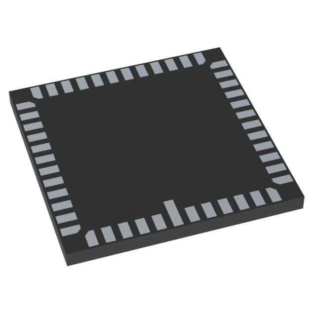
CLCC48 11.43 x 11.43
CASE 848AN
ORDERING INFORMATION
See detailed ordering and shipping information on page 2 of
this data sheet.
• ADC: On-chip, 10-bit Column-parallel
•
•
•
• Array format: Wide-VGA, Active 752 H x 480 V (360,960 Pixels)
• Global Shutter Photodiode Pixels; Simultaneous Integration and
•
•
•
•
•
•
•
•
Readout
RGB Bayer or Monochrome: NIR Enhanced Performance for Use
with Non-visible NIR Illumination
Readout Modes: Progressive or Interlaced
Shutter Efficiency: >99%
Simple Two-wire Serial Interface
Real-Time Exposure Context Switching − Dual Register Set
Register Lock Capability
Window Size: User Programmable to any Smaller Format (QVGA,
CIF, QCIF). Data Rate can be Maintained Independent of Window
Size
Binning: 2 x 2 and 4 x 4 of the Full Resolution
© Semiconductor Components Industries, LLC, 2008
January, 2017 − Rev. 7
1
•
(Option to Operate in 12-bit to 10-bit
Companding Mode)
Automatic Controls: Auto Exposure Control
(AEC) and Auto Gain Control (AGC);
Variable Regional and Variable Weight
AEC/AGC
Support for Four Unique Serial Control
Register IDs to Control Multiple Imagers on
the Same Bus
Data Output Formats:
• Single Sensor Mode:
10-bit Parallel/stand-alone
8-bit or 10-bit Serial LVDS
• Stereo Sensor Mode:
Interspersed 8-bit Serial LVDS
High Dynamic Range (HDR) Mode
Applications
•
•
•
•
•
•
•
Security
High Dynamic Range Imaging
Unattended Surveillance
Stereo Vision
Video as Input
Machine Vision
Automation
Publication Order Number:
MT9V034/D
�MT9V034
Table 1. KEY PERFORMANCE PARAMETERS
Parameter
Value
Optical Format
1/3-inch
Active Imager Size
4.51 mm (H) x 2.88 mm (V)
5.35 mm diagonal
Active Pixels
752 H x 480 V
Pixel Size
6.0 x 6.0 μm
Color Filter Array
Monochrome or color RGB Bayer
Shutter Type
Global Shutter
Maximum Data Rate
Master Clock
27 Mp/s
27 MHz
Full Resolution
752 x 480
Frame Rate
60 fps (at full resolution)
ADC Resolution
10-bit column-parallel
Responsivity
4.8 V/lux-sec (550 nm)
Dynamic Range
>55 dB linear;
>100 dB in HDR mode
Supply Voltage
3.3 V ± 0.3 V (all supplies)
Power Consumption