ON Semiconductor
Is Now
To learn more about onsemi™, please visit our website at
www.onsemi.com
onsemi and and other names, marks, and brands are registered and/or common law trademarks of Semiconductor Components Industries, LLC dba “onsemi” or its affiliates and/or
subsidiaries in the United States and/or other countries. onsemi owns the rights to a number of patents, trademarks, copyrights, trade secrets, and other intellectual property. A listing of onsemi
product/patent coverage may be accessed at www.onsemi.com/site/pdf/Patent-Marking.pdf. onsemi reserves the right to make changes at any time to any products or information herein, without
notice. The information herein is provided “as-is” and onsemi makes no warranty, representation or guarantee regarding the accuracy of the information, product features, availability, functionality,
or suitability of its products for any particular purpose, nor does onsemi assume any liability arising out of the application or use of any product or circuit, and specifically disclaims any and all
liability, including without limitation special, consequential or incidental damages. Buyer is responsible for its products and applications using onsemi products, including compliance with all laws,
regulations and safety requirements or standards, regardless of any support or applications information provided by onsemi. “Typical” parameters which may be provided in onsemi data sheets and/
or specifications can and do vary in different applications and actual performance may vary over time. All operating parameters, including “Typicals” must be validated for each customer application
by customer’s technical experts. onsemi does not convey any license under any of its intellectual property rights nor the rights of others. onsemi products are not designed, intended, or authorized
for use as a critical component in life support systems or any FDA Class 3 medical devices or medical devices with a same or similar classification in a foreign jurisdiction or any devices intended for
implantation in the human body. Should Buyer purchase or use onsemi products for any such unintended or unauthorized application, Buyer shall indemnify and hold onsemi and its officers, employees,
subsidiaries, affiliates, and distributors harmless against all claims, costs, damages, and expenses, and reasonable attorney fees arising out of, directly or indirectly, any claim of personal injury or death
associated with such unintended or unauthorized use, even if such claim alleges that onsemi was negligent regarding the design or manufacture of the part. onsemi is an Equal Opportunity/Affirmative
Action Employer. This literature is subject to all applicable copyright laws and is not for resale in any manner. Other names and brands may be claimed as the property of others.
�N02L83W2A
2Mb Ultra-Low Power Asynchronous CMOS SRAM
256K × 8 bit
Overview
The N02L83W2A is an integrated memory device
containing a 2 Mbit Static Random Access Memory
organized as 262,144 words by 8 bits. The device
is designed and fabricated using ON
Semiconductor’s advanced CMOS technology to
provide both high-speed performance and ultra-low
power. The device operates with two chip enable
(CE1 and CE2) controls and output enable (OE) to
allow for easy memory expansion. The
N02L83W2A is optimal for various applications
where low-power is critical such as battery backup
and hand-held devices. The device can operate
over a very wide temperature range of -40oC to
+85oC and is available in JEDEC standard
packages compatible with other standard 256Kb x
8 SRAMs
Features
• Single Wide Power Supply Range
2.3 to 3.6 Volts
• Very low standby current
2.0µA at 3.0V (Typical)
• Very low operating current
2.0mA at 3.0V and 1µs (Typical)
• Very low Page Mode operating current
0.8mA at 3.0V and 1µs (Typical)
• Simple memory control
Dual Chip Enables (CE1 and CE2)
Output Enable (OE) for memory expansion
• Low voltage data retention
Vcc = 1.8V
• Very fast output enable access time
30ns OE access time
• Automatic power down to standby mode
• TTL compatible three-state output driver
Product Family
Part Number
Package Type
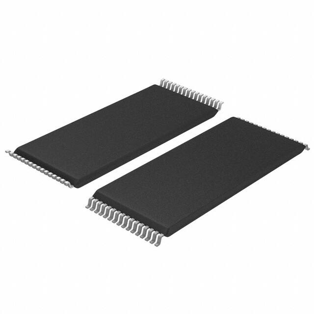
N02L83W2AT
32 - TSOP I
N02L83W2AN
32 - STSOP I
N02L83W2AT2
32 - TSOP I Green
N02L83W2AN2
32 - STSOP I Green
Operating
Power
Temperature Supply (Vcc)
Speed
55ns @ 2.7V
-40oC to +85oC 2.3V - 3.6V 70ns @ 2.3V
Pin Configuration
1
2
3
4
5
6
7
8
9
10
11
12
13
14
15
16
N02L83W2A
STSOP-I, TSOP-I
©2008 SCILLC. All rights reserved.
July 2008 - Rev. 8
2 µA
2 mA @ 1MHz
Pin Descriptions
Pin Name
A11
A9
A8
A13
WE
CE2
A15
VCC
A17
A16
A14
A12
A7
A6
A5
A4
Standby
Operating
Current (ISB), Current (Icc),
Typical
Typical
32
31
30
29
28
27
26
25
24
23
22
21
20
19
18
17
OE
A10
CE1
I/O7
I/O6
I/O5
I/O4
I/O3
VSS
I/O2
I/O1
I/O0
A0
A1
A2
A3
Pin Function
A0-A17
Address Inputs
WE
CE1, CE2
OE
I/O0-I/O7
Write Enable Input
Chip Enable Input
Output Enable Input
Data Inputs/Outputs
VCC
Power
VSS
Ground
Publication Order Number:
N02L83W2A/D
�N02L83W2A
Functional Block Diagram
Word
Address
Decode
Logic
Address
Inputs
A4 - A17
Page
Address
Decode
Logic
CE1
CE2
WE
OE
Control
Logic
16K Page
x 16 word
x 8 bit
RAM Array
Word Mux
Address
Inputs
A0 - A3
Input/
Output
Mux
and
Buffers
I/O0 - I/O7
Functional Description
CE1
CE2
WE
OE
I/O0 - I/O7
MODE
H
X
X
X
High Z
Standby1
Standby
1
X
L
POWER
X
X
High Z
Standby
Standby
Data In
Write2
Active
L
H
L
X2
L
H
H
L
Data Out
Read
Active
L
H
H
H
High Z
Active
Active
1. When the device is in standby mode, control inputs (WE and OE), address inputs and data input/outputs are internally isolated
from any external influence and disabled from exerting any influence externally.
2. When WE is invoked, the OE input is internally disabled and has no effect on the circuit.
Capacitance1
Item
Symbol
Test Condition
Max
Unit
25oC
Min
8
pF
8
pF
Input Capacitance
CIN
VIN = 0V, f = 1 MHz, TA =
I/O Capacitance
CI/O
VIN = 0V, f = 1 MHz, TA = 25oC
1. These parameters are verified in device characterization and are not 100% tested
Rev. 8 | Page 2 of 10 | www.onsemi.com
�N02L83W2A
Absolute Maximum Ratings1
Item
Symbol
Rating
Unit
Voltage on any pin relative to VSS
VIN,OUT
–0.3 to VCC+0.3
V
Voltage on VCC Supply Relative to VSS
VCC
–0.3 to 4.5
V
Power Dissipation
PD
500
mW
Storage Temperature
TSTG
–40 to 125
oC
Operating Temperature
TA
-40 to +85
oC
Soldering Temperature and Time
TSOLDER
260oC, 10sec
oC
1. Stresses greater than those listed above may cause permanent damage to the device. This is a stress rating only and functional
operation of the device at these or any other conditions above those indicated in the operating section of this specification is not
implied. Exposure to absolute maximum rating conditions for extended periods may affect reliability.
Operating Characteristics (Over Specified Temperature Range)
Typ1
Max
Unit
2.3
3.0
3.6
V
Symbol
Supply Voltage
VCC
Data Retention Voltage
VDR
Input High Voltage
VIH
1.8
VCC+0.3
V
Input Low Voltage
VIL
–0.3
0.6
V
Output High Voltage
VOH
IOH = 0.2mA
Output Low Voltage
VOL
IOL = -0.2mA
0.2
V
Input Leakage Current
ILI
VIN = 0 to VCC
0.5
µA
Output Leakage Current
ILO
OE = VIH or Chip Disabled
0.5
µA
Read/Write Operating Supply Current
@ 1 µs Cycle Time2
ICC1
VCC=3.6 V, VIN=VIH or VIL
Chip Enabled, IOUT = 0
2.0
4.0
mA
Read/Write Operating Supply Current
@ 70 ns Cycle Time2
ICC2
VCC=3.6 V, VIN=VIH or VIL
Chip Enabled, IOUT = 0
12.0
16.0
mA
Page Mode Operating Supply Current
@ 70 ns Cycle Time2 (Refer to Power
Savings with Page Mode Operation
diagram)
ICC3
VCC=3.6 V, VIN=VIH or VIL
Chip Enabled, IOUT = 0
4.0
Read/Write Quiescent Operating Supply Current3
ICC4
VCC=3.6 V, VIN=VIH or VIL
Chip Enabled, IOUT = 0,
f=0
ISB1
VIN = VCC or 0V
Chip Disabled
tA= 85oC, VCC = 3.6 V
Maximum Standby
Current3
Maximum Data Retention Current3
IDR
Test Conditions
Min.
Item
Chip Disabled3
VCC = 1.8V, VIN = VCC or 0
Chip Disabled, tA= 85oC
1.8
V
VCC–0.2
V
2.0
mA
3.0
mA
20.0
µA
10.0
µA
1. Typical values are measured at Vcc=Vcc Typ., TA=25°C and not 100% tested.
2. This parameter is specified with the outputs disabled to avoid external loading effects. The user must add current required to drive
output capacitance expected in the actual system.
3. This device assumes a standby mode if the chip is disabled (CE1 high or CE2 low). In order to achieve low standby current all
inputs must be within 0.2 volts of either VCC or VSS.
Rev. 8 | Page 3 of 10 | www.onsemi.com
�N02L83W2A
Power Savings with Page Mode Operation (WE = VIH)
Page Address (A4 - A17)
Word Address (A0 - A3)
Open page
Word 1
Word 2
...
Word 16
CE1
CE2
OE
Note: Page mode operation is a method of addressing the SRAM to save operating current. The internal
organization of the SRAM is optimized to allow this unique operating mode to be used as a valuable power
saving feature.
The only thing that needs to be done is to address the SRAM in a manner that the internal page is left open
and 8-bit words of data are read from the open page. By treating addresses A0-A3 as the least significant
bits and addressing the 16 words within the open page, power is reduced to the page mode value which is
considerably lower than standard operating currents for low power SRAMs.
Rev. 8 | Page 4 of 10 | www.onsemi.com
�N02L83W2A
Timing Test Conditions
Item
Input Pulse Level
0.1VCC to 0.9 VCC
Input Rise and Fall Time
5ns
Input and Output Timing Reference Levels
0.5 VCC
Output Load
CL = 30pF
Operating Temperature
-40 to +85 oC
Timing
2.3 - 3.6 V
2.7 - 3.6 V
Item
Symbol
Read Cycle Time
tRC
Address Access Time
tAA
70
55
ns
Chip Enable to Valid Output
tCO
70
55
ns
Output Enable to Valid Output
tOE
35
30
ns
Chip Enable to Low-Z output
tLZ
10
10
ns
Output Enable to Low-Z Output
tOLZ
5
5
ns
Chip Disable to High-Z Output
tHZ
0
20
0
15
ns
Output Disable to High-Z Output
tOHZ
0
20
0
15
ns
Output Hold from Address Change
tOH
10
10
ns
Write Cycle Time
tWC
70
55
ns
Chip Enable to End of Write
tCW
50
45
ns
Address Valid to End of Write
tAW
50
45
ns
Write Pulse Width
tWP
40
35
ns
Address Setup Time
tAS
0
0
ns
Write Recovery Time
tWR
0
0
ns
Min.
Max.
70
Min.
Max.
55
Units
ns
Write to High-Z Output
tWHZ
Data to Write Time Overlap
tDW
40
35
ns
Data Hold from Write Time
tDH
0
0
ns
End Write to Low-Z Output
tOW
5
5
ns
20
Rev. 8 | Page 5 of 10 | www.onsemi.com
15
ns
�N02L83W2A
Timing of Read Cycle (CE1 = OE = VIL, WE = CE2 = VIH)
tRC
Address
tAA
tOH
Data Out
Previous Data Valid
Data Valid
Timing Waveform of Read Cycle (WE=VIH)
tRC
Address
tAA
tHZ
CE1
tCO
CE2
tLZ
tOHZ
tOE
OE
tOLZ
Data Out
High-Z
Data Valid
Rev. 8 | Page 6 of 10 | www.onsemi.com
�N02L83W2A
Timing Waveform of Write Cycle (WE control)
tWC
Address
tWR
tAW
CE1
tCW
CE2
tAS
tWP
WE
tDW
High-Z
tDH
Data Valid
Data In
tWHZ
tOW
High-Z
Data Out
Timing Waveform of Write Cycle (CE1 Control)
tWC
Address
tWR
tAW
CE1
(for CE2 Control, use
inverted signal)
tAS
tCW
tWP
WE
tDW
Data Valid
Data In
tLZ
Data Out
tDH
tWHZ
High-Z
Rev. 8 | Page 7 of 10 | www.onsemi.com
�N02L83W2A
32-Lead TSOP-I Package (T32)
18.40±0.10
0.50mm REF
8.0±0.10
0.27
0.17
20.0±0.20
SEE DETAIL B
DETAIL B
1.10±0.15
0o-8o
0.20
0.00
0.80mm REF
Note:
1. All dimensions in millimeters
2. Package dimensions exclude molding flash
Rev. 8 | Page 8 of 10 | www.onsemi.com
�N02L83W2A
32-Lead STSOP-I Package (N32)
11.80±0.10
0.50mm REF
8.0±0.10
0.27
0.17
13.40±0.20
SEE DETAIL B
DETAIL B
1.10±0.15
0o-8o
0.20
0.00
0.80mm REF
Note:
1. All dimensions in millimeters
2. Package dimensions exclude molding flash
Rev. 8 | Page 9 of 10 | www.onsemi.com
�N02L83W2A
Ordering Information
Part Number
Package
Shipping Method
N02L83W2AT5I
Leaded 32-TSOP I
Tray
N02L83W2AT25I
Green 32-TSOP I (RoHS Compliant)
Tray
N02L83W2AN5I
Leaded 32-sTSOP I
Tray
N02L83W2AN25I
Green 32-sTSOP I (RoHS Compliant)
Tray
N02L83W2AT5IT
Leaded 32-TSOP I
Tape & Reel
N02L83W2AT25IT
Green 32-TSOP I (RoHS Compliant)
Tape & Reel
N02L83W2AN5IT
Leaded 32-sTSOP I
Tape & Reel
N02L83W2AN25IT
Green 32-sTSOP I (RoHS Compliant)
Tape & Reel
Revision History
Revision #
Date
A
Jan 2001
Initial Advance Release
Mar 2001
Added Table 3: Capacitance
Revised quiescent operating current, changed pin 31 to CE1, modified
table 1 and figure 2, other minor edits
C
Dec. 2001
Part number change from EM256L08, modified Overview and Features, added
Page Mode Operation diagram and Package diagram, revised Operating Characteristics table, Functional Description table, Timing diagrams, and Ordering
Information diagram
D
Nov. 2002
Replaced Isb and Icc on Product Family table with typical values
B
Change Description
E
Oct. 2004
Added Green Package Option
F
Dec. 2005
RoHS Compliant added onto Green packages
G
8
September 2006 Converted to AMI Semiconductor
July 2008
Converted to ON Semiconductor and new part numbers
ON Semiconductor and
are registered trademarks of Semiconductor Components Industries, LLC (SCILLC). SCILLC reserves the right to make changes without
further notice to any products herein. SCILLC makes no warranty, representation or guarantee regarding the suitability of its products for any particular purpose, nor does
SCILLC assume any liability arising out of the application or use of any product or circuit, and specifically disclaims any and all liability, including without limitation special,
consequential or incidental damages. “Typical” parameters which may be provided in SCILLC data sheets and/or specifications can and do vary in different applications
and actual performance may vary over time. All operating parameters, including “Typicals” must be validated for each customer application by customer's technical
experts. SCILLC does not convey any license under its patent rights nor the rights of others. SCILLC products are not designed, intended, or authorized for use as
components in systems intended for surgical implant into the body, or other applications intended to support or sustain life, or for any other application in which the failure
of the SCILLC product could create a situation where personal injury or death may occur. Should Buyer purchase or use SCILLC products for any such unintended or
unauthorized application, Buyer shall indemnify and hold SCILLC and its officers, employees, subsidiaries, affiliates, and distributors harmless against all claims, costs,
damages, and expenses, and reasonable attorney fees arising out of, directly or indirectly, any claim of personal injury or death associated with such unintended or
unauthorized use, even if such claim alleges that SCILLC was negligent regarding the design or manufacture of the part. SCILLC is an Equal Opportunity/Affirmative
Action Employer. This literature is subject to all applicable copyright laws and is not for resale in any manner.
PUBLICATION ORDERING INFORMATION
LITERATURE FULFILLMENT:
Literature Distribution Center for ON Semiconductor
PO Box 5163, Denver, Colorado 80217 USA
Phone: 303-675-2175 or 800-344-3860 Toll Free USA/Canada
Fax: 303-675-2176 or 800-344-3867 Toll Free USA/Canada
Email: orderlit@onsemi.com
N. American Technical Support: 800-282-9855 Toll
Free USA/Canada
Europe, Middle East & Africa Technical Support:
Phone 421-33-790-2910
Japan Customer Focus Center:
Phone 81-3-5773-3850
Rev. 8 | Page 10 of 10 | www.onsemi.com
ON Semiconductor Website: www.onsemi.com
Order Literature: http://www.onsemi.com/orderlit
For additional information, please contact your local
Sales Representative
�


 工商网监
湘ICP备2023018690号
工商网监
湘ICP备2023018690号
