NBA3N012C
3.3 V Automotive Grade
LVDS Line Receiver
Description
The NBA3N012C is a single LVCMOS Output Differential Line
Receiver for Low Power and high data rate Automotive applications.
The device is optimized to support data rate higher than 400 Mbps
(200 MHz). The NBA3N012C accept directly LVDS signal as an input
and translate it to LVCMOS output levels. The device includes an
input termination resistor minimizing number of the external
components for point to point interface.
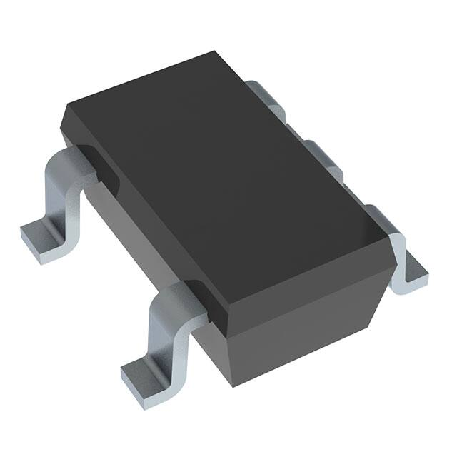
The NBA3N012C is offered in 5 lead SOT23 package and it is
shipping in 3000 pcs tape & reel.
Features
•
•
•
•
•
•
•
•
•
•
•
•
•
Compatible with TIA/EIA−644A Standard
Automotive Grade AECQ−100 Grade 1
> 400 Mbps (200 MHz) Data Rate
Operating Range: VDD = 3.3 V ± 0.3 V
Typical 100 ps Differential Skew
Maximum Propagation Delay of 3.5 ns
Low Power Dissipation (Typical 20 mW @ 3.3 V)
SOT23−5 Lead Package with Pinout optimized for easy PCB Layout
Integrated Line Termination Resistor of 100 W
Power Down High Impedance on LVDS Pins
Inputs Accept LVDS/CML/LVPECL Signals
Temperature Operating Range −40°C to +125°C
These are Pb−Free Devices
www.onsemi.com
MARKING
DIAGRAM
5
SOT23−5
DT SUFFIX
CASE 527AH
12CAYWG
G
1
12C
A
Y
W
G
= Specific Device Code
= Assembly Code
= Year
= Work Week
= Pb−Free Package
(Note: Microdot may be in either location)
LOGIC DIAGRAM
IN
Q
R
IN
Typical Applications:
• Automotive: Head Lamp Lighting for Cars
• Telecom: Wireless, Microwave and Optical
PINOUT DIAGRAM
Table 1. PIN DESCRIPTION
Pin Number
Pin Name
I/O Type
Description
1
VDD
Power Supply Pin
2
GND
Ground Pin
3
IN
Input
Non−Inverting Input Pin
4
IN
Input
Inverting Input Pin
5
Q
Output
Output Pin
Table 2. TRUTH TABLE
Output
[IN] – [IN]
Q
VID ≥ +0.1 V
H
VID ≤ −0.1 V
L
Full Fail Safe OPEN/SHORT or terminated
H or L
December, 2016 − Rev. 0
1
GND
2
IN
3
5
Q
4
IN
ORDERING INFORMATION
Inputs
© Semiconductor Components Industries, LLC, 2016
VDD
Device
Package
Shipping†
NBA3N012CSNT1G
SOT23−5
(Pb−Free)
3000 / Tape &
Reel
†For information on tape and reel specifications,
including part orientation and tape sizes, please
refer to our Tape and Reel Packaging Specification
Brochure, BRD8011/D.
1
Publication Order Number:
NBA3N012C/D
�NBA3N012C
Table 3. ATTRIBUTES (Note 1)
Characteristics
ESD Protection
Value
Human Body Model (JEDEC Standard 22, Method A114−E)
All Pins
≥ 8 kV
Charge Device Model (JEDEC Standard 22, Method C101D)
All Pins
≥ 1.25 kV
Moisture Sensitivity (Note 1)
Flammability Rating
Level 1
Oxygen Index: 28 to 34
UL 94 Code V−0 A
0.125 in 28 to 34
1. For additional information, see Application Note AND8003/D
Table 4. MAXIMUM RATINGS (Note 2)
Symbol
Parameter
VDD
Supply voltage
VIN
Input Voltage (IN, IN) LVDS
VQ
Output Voltage (Pin Q) LVCMOS
IOS
Output Short Circuit Current (Pin Q)
Tj
Tstg
Rating
Unit
−0.30 ≤ VDD ≤ +4.0
V
−0.30 to +3.90
V
−0.30 to (VDD + 0.30)
V
−100
mA
135
°C
−65 to +150
°C
Maximum Junction Temperature
Storage Temperature Range
107
°C/W
138.5
°C/W
Lead Temperature Soldering (4 Seconds) – SOLDERRM/D
260
°C
Package Power Dissipation @ 25°C − Derating of 7.22 mW/°C above 25°C
794
mW
qJC
Thermal resistance (Junction−to−Case) – (Note 3)
qJA
Thermal resistance (Junction−to−Ambient) – (Note 3)
Tsol
PD
Stresses exceeding those listed in the Maximum Ratings table may damage the device. If any of these limits are exceeded, device functionality
should not be assumed, damage may occur and reliability may be affected.
2. The maximum ratings applied are individual stress limit values and not valid simultaneously.
3. JEDEC standard multilayer board −2S2P (2 signal 2 power)
Table 5. DC CHARACTERISTICS VDD = 3.3 V ± 0.3 V, GND = 0 V, TA −40°C to +125°C (Note 4)
Symbol
Parameter
Test Conditions
IDD
No Load Supply Current
Pin: VDD; Inputs Open
VOH
Output High Voltage
Pin: Q; IOH = −0.4 mA,
Inputs shorted or terminated, VID = +200 mV
VOL
Output Low Voltage
Pin: Q; IOL = 2 mA, VID = −200 mV
IOS
Output Short Circuit Current
Pin: Q; VQ = 0 V
VCL
Input Clamp Voltage
ICL = −18 mA
Min
2.4
Typ
Max
Unit
5.4
9
mA
3.1
V
0.3
0.5
V
−15
−50
−100
mA
−1.5
−0.7
V
Product parametric performance is indicated in the Electrical Characteristics for the listed test conditions, unless otherwise noted. Product
performance may not be indicated by the Electrical Characteristics if operated under different conditions.
4. − minus sign indicated only direction. Current into the device is defined as positive. IOS is specified as magnitude only.
Table 6. ELECTRICAL CHARACTERISTICS VDD = 3.3 V ± 0.3 V, GND = 0 V, TA −40°C to +125°C, Pin: IN/IN (Note 5)
Symbol
Parameter
VTH
Differential Input High Threshold
VTL
Differential Input Low Threshold
VCM
Offset Voltage
IIN
Input Current
Test Conditions
−100
VDD = 0 V or 3.6 V
VIN = +3.6 V
Differential Input Current
RT
Integrated Termination Resistor
CIN
Input Capacitance
Typ
Max
Unit
+30
+100
mV
−30
0.1
VIN = +2.8 V
VIN = 0 V
IIND
Min
VCM dependent on VDD
VDD = 0 V
VIN = +0.4 V, VIN = +0 V
mV
2.35
V
−10
±1
+10
mA
−10
±1
+10
mA
+20
mA
4.4
mA
−20
3.0
3.9
VIN = +2.4 V, VIN = +2.0 V
IN = IN = GND
5. − minus sign indicated only direction. Current into the device is defined as positive.
www.onsemi.com
2
100
W
3
pF
�NBA3N012C
Table 7. SWITCHING CHARACTERISTICS
VDD = 3.3 V ± 0.3 V, GND = 0 V, TA −40°C to +125°C, F = 1 MHz, ZO = 50 W, tr, tf ≤ 3 ns (0% to 100%) − (Note 6)
Parameters
Min
Typ
Max
Unit
tpHLD
High to Low Differential Propagation Delay
1.0
1.8
3.5
ns
tpLHD
Low to High Differential Propagation Delay
1.0
Symbol
tr
Rise Time – Transition Low to High
tf
Fall Time – Transition High to Low
tSKD(P)
tSKD(PP)1
tSKD(PP)2
fMAX
1.7
3.5
ns
350
800
ps
175
800
ps
Differential Pulse Skew |tpHLD - tpLHD| (Note 7)
0
100
400
ps
Part to Part Skew – (Note 8)
0
0.3
1.0
ns
Part to Part Skew – (Note 9)
0
0.4
2.5
Maximum Operating Frequency – (Note 10)
250
ns
MHz
6. Test Conditions for the above − VID = 200 mV, CL = 15 pF (includes Load & Jig Capacitance), Figures 1 and 2
7. |tPHLD − tPLHD|, is the magnitude difference in differential propagation delay time between the positive going edge and the negative going
edge of the same channel.
8. Differential Part to Part Skew, is defined as the difference between the minimum and maximum specified differential propagation delays. This
specification applies to devices at the same VDD and within 5°C of each other within the operating temperature range.
9. Part to part skew, is the differential channel to channel skew of any event between devices. This specification applies to devices over
recommended operating temperature and voltage ranges, and across process distribution. tSKD2 is defined as |Max − Min| differential
propagation delay.
10. fMAX Input Conditions: tr = tf < 1 ns (0% to 100%), Duty Cycle 50%, differential (1.05 V to 1.35 V Peak to Peak). fMAX Output Conditions:
VOL (Max 0.4 V), VOH (min 2.4 V), Load = 15 pF (stray + probe), Duty Cycle 60%/40%
PARAMETER MEASUREMENT:
IN
Q
50 Ω
Generator
IN
CL
50 Ω
Figure 1. Receiver Propagation Delay & Transition Time Test Circuit
+1.3 V
IN
V ID = 200 mV
0V Differential
+1.2 V
+1.1 V
IN
tpLHD
t pHLD
VOH
80%
Q
1.5 V
20%
tf
tr
VOL
Figure 2. Receiver Propagation Delay & Transition Time Waveforms
www.onsemi.com
3
�MECHANICAL CASE OUTLINE
PACKAGE DIMENSIONS
SOT−23, 5 Lead
CASE 527AH
ISSUE A
DATE 09 JUN 2021
q
q
q
q
q
q1
q2
GENERIC
MARKING DIAGRAM*
XXXM
XXX = Specific Device Code
M = Date Code
*This information is generic. Please refer to
device data sheet for actual part marking.
Pb−Free indicator, “G” or microdot “G”, may
or may not be present. Some products may
not follow the Generic Marking.
DOCUMENT NUMBER:
DESCRIPTION:
98AON34320E
SOT−23, 5 LEAD
Electronic versions are uncontrolled except when accessed directly from the Document Repository.
Printed versions are uncontrolled except when stamped “CONTROLLED COPY” in red.
PAGE 1 OF 1
ON Semiconductor and
are trademarks of Semiconductor Components Industries, LLC dba ON Semiconductor or its subsidiaries in the United States and/or other countries.
ON Semiconductor reserves the right to make changes without further notice to any products herein. ON Semiconductor makes no warranty, representation or guarantee regarding
the suitability of its products for any particular purpose, nor does ON Semiconductor assume any liability arising out of the application or use of any product or circuit, and specifically
disclaims any and all liability, including without limitation special, consequential or incidental damages. ON Semiconductor does not convey any license under its patent rights nor the
rights of others.
© Semiconductor Components Industries, LLC, 2019
www.onsemi.com
�onsemi,
, and other names, marks, and brands are registered and/or common law trademarks of Semiconductor Components Industries, LLC dba “onsemi” or its affiliates
and/or subsidiaries in the United States and/or other countries. onsemi owns the rights to a number of patents, trademarks, copyrights, trade secrets, and other intellectual property.
A listing of onsemi’s product/patent coverage may be accessed at www.onsemi.com/site/pdf/Patent−Marking.pdf. onsemi reserves the right to make changes at any time to any
products or information herein, without notice. The information herein is provided “as−is” and onsemi makes no warranty, representation or guarantee regarding the accuracy of the
information, product features, availability, functionality, or suitability of its products for any particular purpose, nor does onsemi assume any liability arising out of the application or use
of any product or circuit, and specifically disclaims any and all liability, including without limitation special, consequential or incidental damages. Buyer is responsible for its products
and applications using onsemi products, including compliance with all laws, regulations and safety requirements or standards, regardless of any support or applications information
provided by onsemi. “Typical” parameters which may be provided in onsemi data sheets and/or specifications can and do vary in different applications and actual performance may
vary over time. All operating parameters, including “Typicals” must be validated for each customer application by customer’s technical experts. onsemi does not convey any license
under any of its intellectual property rights nor the rights of others. onsemi products are not designed, intended, or authorized for use as a critical component in life support systems
or any FDA Class 3 medical devices or medical devices with a same or similar classification in a foreign jurisdiction or any devices intended for implantation in the human body. Should
Buyer purchase or use onsemi products for any such unintended or unauthorized application, Buyer shall indemnify and hold onsemi and its officers, employees, subsidiaries, affiliates,
and distributors harmless against all claims, costs, damages, and expenses, and reasonable attorney fees arising out of, directly or indirectly, any claim of personal injury or death
associated with such unintended or unauthorized use, even if such claim alleges that onsemi was negligent regarding the design or manufacture of the part. onsemi is an Equal
Opportunity/Affirmative Action Employer. This literature is subject to all applicable copyright laws and is not for resale in any manner.
PUBLICATION ORDERING INFORMATION
LITERATURE FULFILLMENT:
Email Requests to: orderlit@onsemi.com
onsemi Website: www.onsemi.com
◊
TECHNICAL SUPPORT
North American Technical Support:
Voice Mail: 1 800−282−9855 Toll Free USA/Canada
Phone: 011 421 33 790 2910
Europe, Middle East and Africa Technical Support:
Phone: 00421 33 790 2910
For additional information, please contact your local Sales Representative
�