1. 物料型号:
- NBC12439, NBC12439A
2. 器件简介:
- NBC12439和NBC12439A是基于PLL的通用合成时钟源。VCO频率范围为400 MHz至800 MHz,可配置N分频输出,提供16 MHz、8 MHz、4 MHz或2 MHz的输出频率步进。PLL环路滤波器完全集成,无需外部组件。
3. 引脚分配:
- 输入引脚包括XTAL1、XTAL2(晶振输入)、S_LOAD(串行锁存输入)、S_DATA(串行数据输入)、S_CLOCK(串行时钟输入)、P_LOAD(并行锁存输入)、M[6:0](PLL环路分频器输入)、N[1:0](输出分频器输入)、OE(输出使能输入)、FREF_EXT(外部参考输入)、XTAL_SEL(晶振和外部参考选择输入)和PWR_DOWN(电源下拉输入)。
- 输出引脚包括FOUT、FOUT(PECL差分输出)和TEST(CMOS/TTL输出)。
4. 参数特性:
- 最佳输出抖动性能:±20 ps峰峰值。
- 全集成锁相环,内部环路滤波器。
- 并行接口用于编程计数器和输出分频器。
- 串行3线编程接口。
- 晶振输入10 MHz至20 MHz。
- 工作电压范围:3.135 V至5.25 V。
- CMOS和TTL兼容控制输入。
- PECL输出的电源下拉(÷16)。
- 环境工作温度:0°C至70°C(NBC12439)和-40°C至85°C(NBC12439A)。
5. 功能详解:
- 内部振荡器使用外部石英晶振作为频率参考。
- VCO输出通过M分频器和N输出分频器进行配置,以实现所需的输出频率。
- 配置逻辑包括串行和并行两部份,用于配置内部计数器。
- TEST输出提供多个内部节点值的可见性。
6. 应用信息:
- NBC12439和NBC12439A具有完全集成的板上晶振振荡器,以最小化系统实施成本。
- 晶振电路是串联谐振电路,因此需要使用串联谐振晶振以获得最佳性能。
- 电源滤波:NBC12439和NBC12439A对电源噪声敏感,可能需要在PLL_VCC引脚上增加电源滤波器。
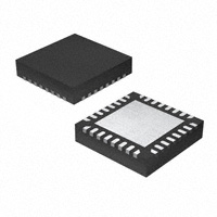
7. 封装信息:
- 提供LQFP-32、PLCC-28和QFN-32封装选项。
- 详细尺寸和标记图在文档的“PACKAGE DIMENSIONS”部分提供。