NBSG14 2.5V/3.3V SiGe Differential 1:4 Clock/Data Driver with RSECL* Outputs
*Reduced Swing ECL
http://onsemi.com Description MARKING DIAGRAMS*
The NBSG14 is a 1−to−4 clock/data distribution chip, optimized for ultra−low skew and jitter. Inputs incorporate internal 50 W termination resistors and accept NECL (Negative ECL), PECL (Positive ECL), LVTTL, LVCMOS, CML, or LVDS. Outputs are RSECL (Reduced Swing ECL), 400 mV.
Features
SG 14 ALYW FCBGA−16 BA SUFFIX CASE 489
16
• • • • •
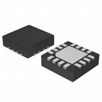
QFN−16 MN SUFFIX CASE 485G
A L Y W G
= Assembly Location = Wafer Lot = Year = Work Week = Pb−Free Package
(Note: Microdot may be in either location) *For additional marking information, refer to Application Note AND8002/D.
ORDERING INFORMATION
See detailed ordering and shipping information in the package dimensions section on page 11 of this data sheet.
© Semiconductor Components Industries, LLC, 2006
1
July, 2006 − Rev. 9
Publication Order Number: NBSG14/D
ÇÇÇ ÇÇÇ
1
• • • • •
Maximum Input Clock Frequency up to 12 GHz Typical Maximum Input Data Rate up to 12 Gb/s Typical 30 ps Typical Rise and Fall Times 125 ps Typical Propagation Delay RSPECL Output with Operating Range: VCC = 2.375 V to 3.465 V with VEE = 0 V RSNECL Output with RSNECL or NECL Inputs with Operating Range: VCC = 0 V with VEE = −2.375 V to −3.465 V RSECL Output Level (400 mV Peak−to−Peak Output), Differential Output 50 W Internal Input Termination Resistors Compatible with Existing 2.5 V/3.3 V LVEP, EP, and LVEL Devices Pb−Free Packages are Available
SG14 ALYWG G
�NBSG14
1 A 2 3 4 VEE 16
VTCLK
Q0 15
Q0 14
VCC 13
Exposed Pad (EP)
Q3
Q3
Q2
VTCLK B
CLK VEE VCC Q2
1 2 NBSG14 3 4
12 Q1 11 Q1 10 Q2 9 Q2
CLK CLK
C
CLK
VEE
VCC
Q1
VTCLK D
VTCLK
Q0
Q0
Q1
5 VEE
6 Q3
7 Q3
8 VCC
Figure 1. BGA−16 Pinout (Top View)
Figure 2. QFN−16 Pinout (Top View)
Table 1. Pin Description
Pin BGA D1 C1 QFN 1 2 Name VTCLK CLK I/O − ECL, CML, LVCMOS, LVDS, LVTTL Input ECL, CML, LVCMOS, LVDS, LVTTL Input − − RSECL Output RSECL Output − RSECL Output RSECL Output RSECL Output RSECL Output RSECL Output RSECL Output − Description Internal 50 W Termination pin. See Table 2. Inverted Differential Input. Internal 75 kW to VEE and 36.5 kW to VCC.
B1
3
CLK
Noninverted Differential Input. Internal 75 kW to VEE.
A1 B2,C2 A2* A3* B3,C3 A4* B4* C4* D4* D3* D2* N/A
4 5,16 6 7 8,13 9 10 11 12 14 15 −
VTCLK VEE Q3 Q3 VCC Q2 Q2 Q1 Q1 Q0 Q0 EP
Internal 50 W Termination Pin. See Table 2. Negative Supply Voltage. All VEE Pins must be Externally Connected to Power Supply to Guarantee Proper Operation. Inverted Differential Output 3. Typically Terminated with 50 W to VTT = VCC − 2 V* Noninverted Differential Output 3. Typically Terminated with 50 W to VTT = VCC − 2 V* Positive Supply Voltage. All VCC Pins must be Externally Connected to Power Supply to Guarantee Proper Operation. Inverted Differential Output 2. Typically Terminated with 50 W to VTT = VCC − 2 V* Noninverted Differential Output 2. Typically Terminated with 50 W to VTT = VCC − 2 V* Inverted Differential Output 1. Typically Terminated with 50 W to VTT = VCC − 2 V* Noninverted Differential Output 1. Typically Terminated with 50 W to VTT = VCC − 2 V* Inverted Differential Output 0. Typically Terminated with 50 W to VTT = VCC − 2 V* Noninverted Differential Output 0. Typically Terminated with 50 W to VTT = VCC − 2 V* Exposed Pad. The thermally exposed pad on package bottom (see case drawing) must be attached to a heat−sinking conduit.
1. In the differential configuration when the input termination pins (VTCLK, VTCLK) are connected to a common termination voltage, if no signal is applied then the device will be susceptible to self−oscillation. *Devices in BGA package typically terminated with 50 W to VTT = VCC − 1.5 V.
http://onsemi.com
2
�NBSG14
VCC Q3 Q3 VTCLK 50 W Q2 CLK CLK 50 W VTCLK 75 KW 75 KW 36.5 KW
Q2
Q1 Q1
VEE
Q0 Q0
Figure 3. Logic Diagram
Table 2. INTERFACING OPTIONS
INTERFACING OPTIONS CML LVDS AC−COUPLED RSECL, PECL, NECL LVTTL, LVCMOS CONNECTIONS Connect VTCLK and VTCLK to VCC Connect VTCLK and VTCLK Together Bias VTCLK and VTCLK Inputs within Common Mode Range (VIHCMR) Standard ECL Termination Techniques An External Voltage (VTHR) should be Applied to the Unused Differential Input. Nominal VTHR is 1.5 V for LVTTL and VCC/2 for LVCMOS Inputs. This Voltage must be within the VTHR Specification.
Table 3. ATTRIBUTES
Characteristics Internal Input Pulldown Resistor (CLK, CLK) Internal Input Pullup Resistor (CLK) ESD Protection Moisture Sensitivity (Note 1) FCBGA−16 QFN−16 Flammability Rating Transistor Count Meets or exceeds JEDEC Spec EIA/JESD78 IC Latchup Test 1. For additional information, see Application Note AND8003/D. Oxygen Index: 28 to 34 Human Body Model Machine Model Pb Pkg Level 3 Level 1 Value 75 kW 36.5 kW > 2 kV > 100 V Pb−Free Pkg N/A Level 1 Value
UL 94 V−0 @ 0.125 in 158
http://onsemi.com
3
�NBSG14
Table 4. MAXIMUM RATINGS
Symbol VCC VEE VI VINPP IIN IOUT TA Tstg qJA Parameter Positive Power Supply Negative Power Supply Positive Input Negative Input Differential Input Voltage |CLK−CLK| Input Current Through RT (50 W Resistor) Output Current Operating Temperature Range Storage Temperature Range Thermal Resistance (Junction−to−Ambient) (Note 2) 0 lfpm 500 lfpm 0 lfpm 500 lfpm 2S2P (Note 2) 2S2P (Note 3) 16 FCBGA 16 FCBGA 16 QFN 16 QFN 16 FCBGA 16 QFN Condition 1 VEE = 0 V VCC = 0 V VEE = 0 V VCC = 0 V VCC − VEE w 2.8 V VCC − VEE < 2.8 V Static Surge Continuous Surge 16 FCBGA 16 QFN VI v VCC VI w VEE Condition 2 Rating 3.6 −3.6 3.6 −3.6 2.8 |VCC−VEE| 45 80 25 50 −40 to +70 −40 to +85 −65 to +150 108 86 41.6 35.2 5 4.0 225 225 Unit V V V V V mA mA mA mA °C °C °C/W °C/W °C/W °C/W °C/W °C/W °C
qJC Tsol
Thermal Resistance (Junction−to−Case) Wave Solder Pb Pb−Free
Stresses exceeding Maximum Ratings may damage the device. Maximum Ratings are stress ratings only. Functional operation above the Recommended Operating Conditions is not implied. Extended exposure to stresses above the Recommended Operating Conditions may affect device reliability. 2. JEDEC standard 51−6, multilayer board − 2S2P (2 signal, 2 power). 3. JEDEC standard multilayer board − 2S2P (2 signal, 2 power) with 8 filled thermal vias under exposed pad.
http://onsemi.com
4
�NBSG14
Table 5. DC CHARACTERISTICS, INPUT WITH RSPECL OUTPUT VCC = 2.5 V; VEE = 0 V (Note 4)
−40°C Symbol IEE VOH VOUTPP VIH VIL VTHR VIHCMR Characteristic Negative Power Supply Current Output HIGH Voltage (Note 5) Output Amplitude Voltage Input HIGH Voltage (Single−Ended) (Notes 7 and 9) Input LOW Voltage (Single−Ended) (Notes 8 and 9) Input Threshold Voltage (Single−Ended) (Note 9) Input HIGH Voltage Common Mode Range (Differential Configuration) (Note 6) Internal Input Termination Resistor Input HIGH Current (@ VIH) Input LOW Current (@ VIL) Min 45 1525 315 VCC− 1435 VIH− 2500 VEE + 1125 1.2 Typ 60 1575 405 VCC− 1000* VCC− 1400* Max 75 1625 495 VCC VIH− 150 VCC− 75 2.5 Min 45 1550 315 VCC− 1435 VIH− 2500 VEE + 1125 1.2 25°C Typ 60 1610 405 VCC− 1000* VCC− 1400* Max 75 1650 495 VCC VIH− 150 VCC− 75 2.5 70°C(BGA)/85°C(QFN)** Min 45 1575 315 VCC− 1435 VIH− 2500 VEE + 1125 1.2 Typ 60 1635 405 VCC− 1000* VCC− 1400* Max 75 1675 495 VCC VIH− 150 VCC− 75 2.5 Unit mA mV mV mV mV mV V
RTIN IIH IIL
45
50 80 25
55 150 100
45
50 80 25
55 150 100
45
50 80 25
55 150 100
W mA mA
NOTE: Device will meet the specifications after thermal equilibrium has been established when mounted in a test socket or printed circuit board with maintained transverse airflow greater than 500 lfpm. Electrical parameters are guaranteed only over the declared operating temperature range. Functional operation of the device exceeding these conditions is not implied. Device specification limit values are applied individually under normal operating conditions and not valid simultaneously. *Typicals used for testing purposes. **The device packaged in FCBGA−16 have maximum temperature specification of 70°C and devices packaged in QFN−16 have maximum temperature specification of 85°C. 4. Input and output parameters vary 1:1 with VCC. VEE can vary +0.125 V to −0.5 V. 5. All outputs loaded with 50 W to VCC − 1.5 V for BGA package and VCC − 2 V for QFN package. VOH/VOL measured at VIH/VIL (Typical). 6. VIHCMR min varies 1:1 with VEE, VIHCMR max varies 1:1 with VCC. The VIHCMR range is referenced to the most positive side of the differential input signal. 7. VIH cannot exceed VCC. |VIH − VTHR| < 2600 mV. 8. VIL always ≥ VEE. |VIL − VTHR| < 2600 mV. 9. VTHR is the voltage applied to one input when running in single−ended mode.
http://onsemi.com
5
�NBSG14
Table 6. DC CHARACTERISTICS, INPUT WITH RSPECL OUTPUT VCC = 3.3 V; VEE = 0 V (Note 10)
−40°C Symbol IEE VOH VOUTPP VIH VIL VTHR VIHCMR Characteristic Negative Power Supply Current Output HIGH Voltage (Note 11) Output Amplitude Voltage Input HIGH Voltage (Single−Ended) (Notes 13 and 15) Input LOW Voltage (Single−Ended) (Notes 14 and 15) Input Threshold Voltage (Single−Ended) (Note 15) Input HIGH Voltage Common Mode Range (Differential Configuration) (Note 12) Internal Input Termination Resistor Input HIGH Current (@ VIH) Input LOW Current (@ VIL) Min 45 2325 350 VCC− 1435 VIH− 2500 VEE + 1125 1.2 Typ 60 2375 440 VCC− 1000* VCC− 1400* Max 75 2425 530 VCC VIH− 150 VCC− 75 3.3 Min 45 2350 350 VCC− 1435 VIH− 2500 VEE + 1125 1.2 25°C Typ 60 2410 440 VCC− 1000* VCC− 1400* Max 75 2450 530 VCC VIH− 150 VCC− 75 3.3 70°C(BGA)/85°C(QFN)** Min 45 2375 350 VCC− 1435 VIH− 2500 VEE + 1125 1.2 Typ 60 2435 440 VCC− 1000* VCC− 1400* Max 75 2475 530 VCC VIH− 150 VCC− 75 3.3 Unit mA mV mV mV mV mV V
RTIN IIH IIL
45
50 80 25
55 150 100
45
50 80 25
55 150 100
45
50 80 25
55 150 100
W mA mA
NOTE: Device will meet the specifications after thermal equilibrium has been established when mounted in a test socket or printed circuit board with maintained transverse airflow greater than 500 lfpm. Electrical parameters are guaranteed only over the declared operating temperature range. Functional operation of the device exceeding these conditions is not implied. Device specification limit values are applied individually under normal operating conditions and not valid simultaneously. *Typicals used for testing purposes. **The device packaged in FCBGA−16 have maximum temperature specification of 70°C and devices packaged in QFN−16 have maximum temperature specification of 85°C. 10. Input and output parameters vary 1:1 with VCC. VEE can vary +0.3 V to −0.165 V. 11. All outputs loaded with 50 W to VCC − 1.5 V for BGA package and VCC − 2 V for QFN package. VOH/VOL measured at VIH/VIL (Typical). 12. VIHCMR min varies 1:1 with VEE, VIHCMR max varies 1:1 with VCC. The VIHCMR range is referenced to the most positive side of the differential input signal. 13. VIH cannot exceed VCC. |VIH − VTHR| < 2600 mV. 14. VIL always ≥ VEE. |VIL − VTHR| < 2600 mV. 15. VTHR is the voltage applied to one input when running in single−ended mode.
http://onsemi.com
6
�NBSG14
Table 7. DC CHARACTERISTICS, NECL OR RSNECL INPUT WITH NECL OUTPUT
VCC = 0 V; VEE = −3.465 V to −2.375 V (Note 16) −40°C Symbol IEE VOH VOUTPP Characteristic Negative Power Supply Current Output HIGH Voltage (Note 17) Output Amplitude Voltage −3.465 V v VEE v −3.0 V −3.0 V < VEE v −2.375 V Input HIGH Voltage (Single−Ended) (Notes 19 and 21) Input LOW Voltage (Single−Ended) (Notes 20 and 21) Input Threshold Voltage (Single−Ended) (Note 21) Input HIGH Voltage Common Mode Range (Differential Configuration) (Note 18) Internal Input Termination Resistor Input HIGH Current (@ VIH) Input LOW Current (@ VIL) Min 45 −975 350 315 VCC− 1435 VIH− 2500 VEE + 1125 VEE + 1.2 Typ 60 −925 440 405 VCC− 1000* VCC− 1400* Max 75 −875 530 495 VCC VIH− 150 VCC− 75 0.0 Min 45 −950 350 315 VCC− 1435 VIH− 2500 VEE + 1125 VEE + 1.2 25°C Typ 60 −890 440 405 VCC− 1000* VCC− 1400* Max 75 −850 530 495 VCC VIH− 150 VCC− 75 0.0 70°C(BGA)/85°C(QFN)** Min 45 −925 350 315 VCC− 1435 VIH− 2500 VEE + 1125 VEE + 1.2 Typ 60 −865 440 405 VCC− 1000* VCC− 1400* Max 75 −825 530 495 VCC VIH− 150 VCC− 75 0.0 mV mV mV V Unit mA mV mV
VIH VIL VTHR VIHCMR
RTIN IIH IIL
45
50 80 25
55 150 100
45
50 80 25
55 150 100
45
50 80 25
55 150 100
W mA mA
NOTE: Device will meet the specifications after thermal equilibrium has been established when mounted in a test socket or printed circuit board with maintained transverse airflow greater than 500 lfpm. Electrical parameters are guaranteed only over the declared operating temperature range. Functional operation of the device exceeding these conditions is not implied. Device specification limit values are applied individually under normal operating conditions and not valid simultaneously. *Typicals used for testing purposes. **The device packaged in FCBGA−16 have maximum temperature specification of 70°C and devices packaged in QFN−16 have maximum temperature specification of 85°C. 16. Input and output parameters vary 1:1 with VCC. 17. All outputs loaded with 50 W to VCC −1.5 V for BGA package and VCC − 2 V for QFN package. VOH/VOL measured at VIH/VIL (Typical). 18. VIHCMR min varies 1:1 with VEE, VIHCMR max varies 1:1 with VCC. The VIHCMR range is referenced to the most positive side of the differential input signal. 19. VIH cannot exceed VCC. |VIH − VTHR| < 2600 mV. 20. VIL always ≥ VEE. |VIL − VTHR| < 2600 mV. 21. VTHR is the voltage applied to one input when running in single−ended mode.
http://onsemi.com
7
�NBSG14
Table 8. AC CHARACTERISTICS for FCBGA−16
VCC = 0 V; VEE = −3.465 V to −2.375 V or VCC = 2.375 V to 3.465 V; VEE = 0 V −40°C Symbol fmax tPLH, tPHL tSKEW Characteristic Maximum Frequency (See Figure 4) (Note 22) Propagation Delay to Output Differential Duty Cycle Skew (Note 23) Within−Device Skew (Note 24) Device−to−Device Skew (Note 25) RMS Random Clock Jitter (Figure 4) (Note 27) fin < 10 GHz Peak−to−Peak Data Dependent Jitter (Note 28) fin < 10 Gb/s Input Voltage Swing/Sensitivity (Differential Configuration) (Note 26) Output Rise/Fall Times (20% − 80%) @ 1 GHz Q, Q 75 20 30 Min 10.7 100 Typ 12 125 2 6 25 0.2 150 10 15 50 1 Max Min 10.7 100 25°C Typ 12 125 2 6 25 0.2 10 2600 55 75 20 30 2600 55 75 20 30 2600 55 mV ps 150 10 15 50 1 Max Min 10.7 100 70°C Typ 12 125 2 6 25 0.2 150 10 15 50 1 Max Unit GHz ps ps
tJITTER
ps
VINPP tr tf
NOTE: Device will meet the specifications after thermal equilibrium has been established when mounted in a test socket or printed circuit board with maintained transverse airflow greater than 500 lfpm. Electrical parameters are guaranteed only over the declared operating temperature range. Functional operation of the device exceeding these conditions is not implied. Device specification limit values are applied individually under normal operating conditions and not valid simultaneously. 22. Measured using a 500 mV source, 50% duty cycle clock source. All outputs loaded with 50 W to VCC − 1.5 V. Input edge rates 40 ps (20% − 80%). 23. See Figure 6. tSKEW = |tPLH − tPHL| for a nominal 50% Differential Clock Input Waveform. 24. Within−Device skew is measured between outputs under identical transitions and conditions on any one device. 25. Device−to−device skew for identical transitions at identical VCC levels. 26. VINPP (MAX) cannot exceed VCC − VEE (applicable only when VCC−VEE < 2600 mV). 27. Additive RMS Jitter with 50% duty cycle clock signal at 10 GHz. 28. Additive Peak−to−Peak data dependent jitter with NRZ PRBS 231−1 data at 10 Gb/s.
http://onsemi.com
8
�NBSG14
Table 9. AC CHARACTERISTICS for QFN−16
VCC = 0 V; VEE = −3.465 V to −2.375 V or VCC = 2.375 V to 3.465 V; VEE = 0 V −40°C Symbol fmax tPLH, tPHL tSKEW Characteristic Maximum Frequency (See Figure 4) (Note 29) Propagation Delay to Output Differential Duty Cycle Skew (Note 30) Within−Device Skew (Note 31) Device−to−Device Skew (Note 32) RMS Random Clock Jitter (Figure 4) (Note 34) fin < 10 GHz Peak−to−Peak Data Dependent Jitter (Note 35) fin < 10 Gb/s Input Voltage Swing/Sensitivity (Differential Configuration) (Note 33) Output Rise/Fall Times (20% − 80%) @ 1 GHz Q, Q 75 15 30 Min 10.5 90 Typ 12 125 3 6 25 0.2 160 15 15 50 1 Max Min 10.5 90 25°C Typ 12 125 3 6 25 0.2 10 2600 55 75 20 30 2600 55 75 20 30 2600 55 mV ps 160 15 15 50 1 Max Min 10.5 90 85°C Typ 12 125 3 6 25 0.2 160 15 15 50 1 Max Unit GHz ps ps
tJITTER
ps
VINPP tr tf
NOTE: Device will meet the specifications after thermal equilibrium has been established when mounted in a test socket or printed circuit board with maintained transverse airflow greater than 500 lfpm. Electrical parameters are guaranteed only over the declared operating temperature range. Functional operation of the device exceeding these conditions is not implied. Device specification limit values are applied individually under normal operating conditions and not valid simultaneously. 29. Measured using a 500 mV source, 50% duty cycle clock source. All outputs loaded with 50 W to VCC − 2.0 V. Input edge rates 40 ps (20% − 80%) 30. See Figure 6. tSKEW = |tPLH − tPHL| for a nominal 50% Differential Clock Input Waveform. 31. Within−Device skew is measured between outputs under identical transitions and conditions on any one device. 32. Device−to−device skew for identical transitions at identical VCC levels. 33. VINPP (MAX) cannot exceed VCC − VEE (applicable only when VCC−VEE < 2600 mV). 34. Additive RMS Jitter with 50% duty cycle clock signal at 10 GHz. 35. Additive Peak−to−Peak data dependent jitter with NRZ PRBS 231−1 data at 10 Gb/s.
http://onsemi.com
9
�NBSG14
500 OUTPUT VOLTAGE AMPLITUDE (mV) 10 9 400 OUTPUT AMPLITUDE 300 8 JITTERout ps (RMS) 7 6 5 4 3 2 1 0
200
100
Figure 5. Eye Diagram at 10.8 Gbps (VCC − VEE = 3.3 V @ 255C with Input Data Pattern of 2^31−1 PRBS. Total Pk−Pk System Jitter Including Signal Generator is 18 ps. This Data was taken by Acquiring 7000 Waveforms.)
ÇÇÇÇÇÇÇÇÇÇÇÇ ÇÇÇÇÇÇÇÇÑÑÑÑÇÇÇÇÇÇ ÇÇÇÇÇÇÇÇÇÇ ÇÇÇÇÇÇÇÇÑÑÑÑÇÇÇÇÇ ÇÇÇÇ ÇÇÇÇÇÇÇÇÇÇÑÑÑÑÑÑÑÇ ÇÇÇÇÇÇÇÇ ÇÇÇÇÇÇÇÇÇÇÑÑÑÑÑÑÑÇ ÇÇÇÇÇÇÇ ÇÇÇÇÇÇÇÇÇÇÑÑÑÑÑÑÑÇ ÇÇÇÇÇÇÇ ÇÇÇÇÇÇÇÇÇÇÇÇÇÇÇÇÇÇ ÇÇÇÇÇÇÇÇÇÇÇÇÇÇÇÇÇÇ
OUTPUT P−P SPEC (AMPLITUDE GUARANTEE) RMS JITTER 0 1 2 3 4 5 6 7 8 9 10 11 12 INPUT FREQUENCY (GHz)
Figure 4. Output Voltage Amplitude (VOUTPP) / RMS Jitter vs. Input Frequency (fin) at Ambient Temperature (Typical)
X = 17 ps/DIV, Y = 53 mV/DIV
http://onsemi.com
10
�NBSG14
D/CLK VINPP = = VIH(CLK) − VIL(CLK) D/CLK Q VOUTPP = VOH(Q) − VOL(Q) Q tPLH tPHL
Figure 6. AC Reference Measurement
Q Driver Device Q
Zo = 50 W
D Receiver Device
Zo = 50 W 50 W 50 W
D
VTT VTT = VCC − 2.0 V
Figure 7. Typical Termination for Output Driver and Device Evaluation (See Application Note AND8020/D − Termination of ECL Logic Devices.)
ORDERING INFORMATION
Device NBSG14BA NBSG14BAR2 NBSG14MN NBSG14MNG NBSG14MNR2 NBSG14MNR2G Package FCBGA−16 FCBGA−16 QFN−16 QFN−16 (Pb−Free) QFN−16 QFN−16 (Pb−Free) Shipping† 100 Units / Tray (Contact Sales Representative) 100 / Tape & Reel 123 Units / Rail 123 Units / Rail 3000 / Tape & Reel 3000 / Tape & Reel
Board NBSG14BAEVB
Description NBSG14BA Evaluation Board
†For information on tape and reel specifications, including part orientation and tape sizes, please refer to our Tape and Reel Packaging Specifications Brochure, BRD8011/D.
http://onsemi.com
11
�NBSG14
PACKAGE DIMENSIONS
LASER MARK FOR PIN 1 IDENTIFICATION IN THIS AREA
FCBGA−16 BA SUFFIX PLASTIC 4X4 (mm) BGA FLIP CHIP PACKAGE CASE 489−01 ISSUE O
−X− D M
NOTES: 1. DIMENSIONS ARE IN MILLIMETERS. 2. INTERPRET DIMENSIONS AND TOLERANCES PER ASME Y14.5M, 1994. 3. DIMENSION b IS MEASURED AT THE MAXIMUM SOLDER BALL DIAMETER, PARALLEL TO DATUM PLANE Z. 4. DATUM Z (SEATING PLANE) IS DEFINED BY THE SPHERICAL CROWNS OF THE SOLDER BALLS. 5. PARALLELISM MEASUREMENT SHALL EXCLUDE ANY EFFECT OF MARK ON TOP SURFACE OF PACKAGE. DIM A A1 A2 b D E e S MILLIMETERS MIN MAX 1.40 MAX 0.25 0.35 1.20 REF 0.30 0.50 4.00 BSC 4.00 BSC 1.00 BSC 0.50 BSC
−Y− K E
M 0.20
3X FEDUCIAL FOR PIN A1 IDENTIFICATION IN THIS AREA A B C D
e
4
3
2
1
3
16 X
b 0.15 0.08
M M
S VIEW M−M
ZXY Z
5 0.15 Z A A2 −Z−
A1
16 X
4 DETAIL K
0.10 Z
ROTATED 90 _ CLOCKWISE
http://onsemi.com
12
�NBSG14
PACKAGE DIMENSIONS
16 PIN QFN CASE 485G−01 ISSUE C
NOTES: 1. DIMENSIONING AND TOLERANCING PER ASME Y14.5M, 1994. 2. CONTROLLING DIMENSION: MILLIMETERS. 3. DIMENSION b APPLIES TO PLATED TERMINAL AND IS MEASURED BETWEEN 0.25 AND 0.30 MM FROM TERMINAL. 4. COPLANARITY APPLIES TO THE EXPOSED PAD AS WELL AS THE TERMINALS. 5. Lmax CONDITION CAN NOT VIOLATE 0.2 MM MINIMUM SPACING BETWEEN LEAD TIP AND FLAG MILLIMETERS MIN MAX 0.80 1.00 0.00 0.05 0.20 REF 0.18 0.30 3.00 BSC 1.65 1.85 3.00 BSC 1.65 1.85 0.50 BSC 0.18 TYP 0.30 0.50
D
A B
PIN 1 LOCATION
0.15 C 0.15 C 0.10 C TOP VIEW
16 X
0.08 C SIDE VIEW A1 C
16X
L
5
NOTE 5 4
16X
K
1 12
16X
b BOTTOM VIEW
0.10 C A B 0.05 C
NOTE 3
ON Semiconductor and are registered trademarks of Semiconductor Components Industries, LLC (SCILLC). SCILLC reserves the right to make changes without further notice to any products herein. SCILLC makes no warranty, representation or guarantee regarding the suitability of its products for any particular purpose, nor does SCILLC assume any liability arising out of the application or use of any product or circuit, and specifically disclaims any and all liability, including without limitation special, consequential or incidental damages. “Typical” parameters which may be provided in SCILLC data sheets and/or specifications can and do vary in different applications and actual performance may vary over time. All operating parameters, including “Typicals” must be validated for each customer application by customer’s technical experts. SCILLC does not convey any license under its patent rights nor the rights of others. SCILLC products are not designed, intended, or authorized for use as components in systems intended for surgical implant into the body, or other applications intended to support or sustain life, or for any other application in which the failure of the SCILLC product could create a situation where personal injury or death may occur. Should Buyer purchase or use SCILLC products for any such unintended or unauthorized application, Buyer shall indemnify and hold SCILLC and its officers, employees, subsidiaries, affiliates, and distributors harmless against all claims, costs, damages, and expenses, and reasonable attorney fees arising out of, directly or indirectly, any claim of personal injury or death associated with such unintended or unauthorized use, even if such claim alleges that SCILLC was negligent regarding the design or manufacture of the part. SCILLC is an Equal Opportunity/Affirmative Action Employer. This literature is subject to all applicable copyright laws and is not for resale in any manner.
PUBLICATION ORDERING INFORMATION
LITERATURE FULFILLMENT: Literature Distribution Center for ON Semiconductor P.O. Box 5163, Denver, Colorado 80217 USA Phone: 303−675−2175 or 800−344−3860 Toll Free USA/Canada Fax: 303−675−2176 or 800−344−3867 Toll Free USA/Canada Email: orderlit@onsemi.com N. American Technical Support: 800−282−9855 Toll Free USA/Canada Europe, Middle East and Africa Technical Support: Phone: 421 33 790 2910 Japan Customer Focus Center Phone: 81−3−5773−3850 ON Semiconductor Website: www.onsemi.com Order Literature: http://www.onsemi.com/orderlit For additional information, please contact your local Sales Representative
ÇÇ ÇÇ ÇÇ
(A3) D2 e
8 9 16 13
E
DIM A A1 A3 b D D2 E E2 e K L
A
SEATING PLANE
SOLDERING FOOTPRINT*
3.25 0.128 0.30 0.012
0.575 0.022
EXPOSED PAD
EXPOSED PAD
E2 e
3.25 0.128
1.50 0.059
0.50 0.02
0.30 0.012
SCALE 10:1 mm inches
*For additional information on our Pb−Free strategy and soldering details, please download the ON Semiconductor Soldering and Mounting Techniques Reference Manual, SOLDERRM/D.
http://onsemi.com
13
NBSG14/D
�


 工商网监
湘ICP备2023018690号
工商网监
湘ICP备2023018690号
