NCN8024
Smart Card Interface IC
The NCN8024 is a single smart card interface IC. It is dedicated for
3.0 V/5.0 V smart card reader/writer applications.
The device is fully compatible with the ISO 7816−3 and EMV
standards as well as with standards specifying conditional access in
Set−Top−Box (STB) including NDS.
For details regarding device implementation refer to application
note AND8452/D, available upon request (please contact your local
ON Semiconductor sales office or representative).
http://onsemi.com
MARKING
DIAGRAMS
Features
28
• Single IC Card Interface
• Fully Compatible with ISO 7816−3, EMV and Related Standards
•
•
•
•
•
•
•
•
•
•
•
•
•
Including NDS
Three Bidirectional Buffered I/O Level Shifters (C4, C7 and C8 Card
Pins)
3.0 V or 5.0 V ± 5% Regulated Card Power Supply such as ICC ≤
75 mA at 3.3 V ≤ VDDP ≤ 5.5 V
Independent Power Supply Range on Controller Interface
(2.7 V < VDD < 5.5 V)
Handles 3.0 V and 5.0 V Smart Cards
Thermal and Short Circuit Protection on all Card Pins
Support up to 18 MHz Clock with Internal Division Ratio 1/1, 1/2,
1/4 and 1/8 through CLKDIV1 and CLKDIV2 Pins
ESD Protection on Card Pins up to 8 kV+ (Human Body Model)
Activation/Deactivation Sequences (ISO7816)
Fault Protection Mechanisms Enabling Automatic Device
Deactivation in Case of Overload, Overheating, Card Take−off or
Power Supply Drop−out
Interrupt Signal INT for Card Presence and Faults
External Undervoltage Lockout Threshold Adjustment on VDD
(PORADJ Pin)
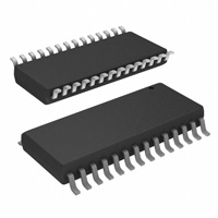
Available in 2 Package Formats: SOIC−28 and TSSOP−28
These are Pb−Free Devices
SOIC−28
CASE 751F
TSSOP−28
CASE 948AA
1
NCN
8024G
ALYW
NCN8024 = Specific Device Code
A
= Assembly Location
WL, L = Wafer Lot
YY, Y
= Year
WW, W = Work Week
G
= Pb−Free Package
ORDERING INFORMATION
See detailed ordering and shipping information in the package
dimensions section on page 14 of this data sheet.
Typical Application
•
•
•
•
NCN8024
AWLYYWWG
Set−Top Boxes Conditional Access & Pay−TV
Conditional Access Modules (CAM)
POS / ATM
Access Control, Identification
© Semiconductor Components Industries, LLC, 2012
October, 2012 − Rev. 4
1
Publication Order Number:
NCN8024/D
�NCN8024
VDDP
10 uF
100 nF
100 nF
VDD
100 nF
VDDP
Microcontroller
VDD
VDD
R1
CRD_PRES
CMDVCC
5V/3V
CLKDIV1
CRD_VCC
CRD_RST
CLKIN
CRD_CLK
CRD_AUX1
CRD_AUX2
CRD_IO
RSTIN
CRD_GND
CLKDIV2
100 nF
CRD_PRES
PORADJ
NCN8024
CONTROL
C2
VUP
INT
R2
DATAPORT
C1
I/Ouc
SMART CARD
GND
220 nF
GND
330 nF
1
2
3
4
GNDP
AUX1uc
AUX2uc
GND
GND
Figure 1. Typical Smart Card Interface Application
CLKDIV1
1
28
AUX2uc
CLKDIV2
2
27
AUX1uc
5V/3V
3
26
I/Ouc
GNDP
4
25
NC
C2
5
24
CLKIN
VDDP
6
23
INT
C1
7
22
GND
VUP
8
21
VDD
CRD_PRES
9
20
RSTIN
CRD_PRES
10
19
CMDVCC
CRD_I/O
11
18
PORADJ
CRD_AUX2
12
17
CRD_VCC
CRD_AUX1
13
16
CRD_RST
14
15
CRD_CLK
CRD_GND
Figure 2. SOIC−28 and TSS0P−28 Pinout (Top View)
http://onsemi.com
2
DET
DET
Vcc
RST
CLK
C4
GND
Vpp
I/O
C8
5 GND
6
7
8
�NCN8024
VDDP
VDD
21
6
9 CRD_PRES
Interrupt Block
INT 23
Card Detection
10 CRD_PRES
5V/3V
Supply Voltage
Monitoring
3
CMDVCC 19
PORADJ
18
CLKDIV1
1
CLKDIV2
2
DC/DC Converter
5
C2
7
C1
Internal Oscillator 2.5 MHz
17 CRD_VCC
Thermal Control
4
GNDP
8
VUP
CLKIN
24
NC
25
RSTIN
20
I/Ouc
26
11 CRD_I/O
AUX2uc
27
13 CRD_AUX2
AUX1uc
28
12 CRD_AUX1
GND
22
14 CRD_GND
Clock Dividers
15 CRD_CLK
Control Logic
and Sequencer
Card Pin
Drivers
16 CRD_RST
Figure 3. NCN8024 Block Diagram
PIN FUNCTION AND DESCRIPTION
Pin #
Name
Type
Description
1
CLKDIV1
Input
This pin coupled with CLKDIV2 is used to program the clock frequency division ratio (Table 1).
2
CLKDIV2
Input
This pin coupled with CLKDIV1 is used to program the clock frequency division ratio (Table 1).
3
5V/3V
Input
Allows selecting card VCC power supply voltage. CRD_VCC = 5 V when 5V/3V = HIGH or 3 V when
5V/3V = LOW
4
GNDP
GND
DC/DC Converter Power Supply Ground
5
C2
Power
DC/DC Converter Capacitor pin number 2 − A 100 nF capacitor is connected between this pin and
pin C1. The capacitor has to feature an ESR lower than 100 mW
6
VDDP
Power
DC/DC Converter Power Supply Voltage
7
C1
Power
DC/DC Converter Capacitor pin number 1 − A 100 nF capacitor is connected between this pin and
pin C2. The capacitor has to feature an ESR lower than 100 mW
8
VUP
Power
Charge−pump output − a very low ESR 100 nF capacitor (ESR< 100 mW) is connected between
this pin and GNDP
9
CRD_PRES
Input
Card presence pin active (card present) when CRD_PRES = Low. A built−in debounce timer of
about 8 ms is activated when a card is inserted.
10
CRD_PRES
Input
Card presence pin active (card present) when CRD_PRES = High. A built−in debounce timer of
about 8 ms is activated when a card is inserted.
http://onsemi.com
3
�NCN8024
PIN FUNCTION AND DESCRIPTION
Pin #
Name
Type
Description
11
CRD_I/O
Input/
Output
This pin handles the connection to the serial I/O (C7) of the card connector. A bi−directional level
translator adapts the serial I/O signal between the card and the micro controller. An 11 kW (typical)
pullup resistor to CRD_VCC provides a High impedance state for the smart card I/O link.
12
CRD_AUX2
Input/
Output
This pin handles the connection to the chip card’s serial auxiliary AUX2 I/O pin (C8). A bi−directional
level translator adapts the serial I/O signal between the card and the micro controller. An 11 kW
(typical) pullup resistor to CRD_VCC provides a High impedance state for the smart card C8 pin.
13
CRD_AUX1
Input/
Output
This pin handles the connection to the chip card’s serial auxiliary AUX1 I/O pin (C4). A bi−directional
level translator adapts the serial I/O signal between the card and the micro controller. An 11 kW
(typical) pullup resistor to CRD_VCC provides a High impedance state for the smart card C4 pin.
14
CRD_GND
GND
15
CRD_CLK
Output
This pin is connected to the CLOCK card connector’s pin (Chip card’s pin C3). The Clock signal
comes from the CLKIN input through clock dividers and level shifter.
16
CRD_RST
Output
This pin is connected to the chip card’s RESET pin (C2) through the card connector. A level
translator adapts the external Reset (RSTIN) signal to the smart card.
17
CRD_VCC
Power
This pin is connected to the smart card power supply pin. An internal DC/DC converter is
programmable using the pin 5V/3V to supply either 5 V or 3 V output voltage. An external distributed
ceramic capacitor (200 nF + 330 nF typical recommended) must be connected across CRD_VCC
and CRD_GND. This set of capacitor (if distributed) must be low ESR (< 100 mW).
18
PORADJ
Input
Power−on reset threshold adjustment input pin for changing the reset threshold with an external
resistor power divider. Recommended to be connected to ground when unused.
19
CMDVCC
Input
Command VCC pin. Activation sequence Enable/Disable pin (active Low). The activation sequence is
enabled by toggling CMDVCC High to Low and when a card is present.
20
RSTIN
Input
This Reset input connected to the host and referred to VDD (microcontroller side), is connected to
the smart card Reset pin through the internal level shifter which translates the level according to the
CRD_VCC programmed value.
21
VDD
Power
22
GND
GND
23
INT
Output
24
CLKIN
Input
25
NC
26
I/Ouc
Input/
Output
This pin is connected to an external micro−controller. A bi−directional level translator adapts the
serial I/O signal between the smart card and the external controller. A built−in constant 11 kW
(typical) resistor provides a high impedance state.
27
AUX1uc
Input/
Output
This pin is connected to an external micro−controller. A bi−directional level translator adapts the
serial C4 signal between the smart card and the external controller. A built−in constant 11 kW
(typical) resistor provides a high impedance state.
28
AUX2uc
Input/
Output
This pin is connected to an external micro−controller. A bi−directional level translator adapts the
serial C8 signal between the smart card and the external controller. A built−in constant 11 kW
(typical) resistor provides a high impedance state.
Card Ground
This pin is connected to the system controller power supply. It configures the level shifter input
stage to accept the signals coming from the controller. A 0.1 mF capacitor shall be used to bypass
the power supply voltage. When VDD is below 2.35 V typical the card pins are disabled.
Ground
The interrupt request is activated LOW on this pin. This is enabled when a card is present and the
card presence is detected by CRD_PRES or CRD_PRES pins. Similarly an interrupt is generated
when CRD_VCC is overloaded. 20 kW typical integrated pullup resistor to VDD.
Clock Input for External Clock
Unconnected
http://onsemi.com
4
�NCN8024
ATTRIBUTES
Characteristics
Values
ESD protection
Human Body Model (HBM) (Note 1)
Card Pins (Card Interface Pins 9 − 17)
All Other Pins
Machine Model (MM)
Card Pins (Card Interface Pins 9 − 17)
All Other Pins
Moisture sensitivity (Note 2) SOIC−28 and TSSOP−28
Flammability Rating Oxygen
8 kV
2 kV
400 V
150 V
Level 3
Index: 28 to 34
UL 94 V−0 @ 0.125 in
Meets or exceeds JEDEC Spec EIA/JESD78 IC Latch−up Test
1. Human Body Model (HBM), R = 1500 W, C = 100 pF.
2. For additional information, see Application Note AND8003/D.
MAXIMUM RATINGS (Note 3)
Rating
Symbol
Value
Unit
DC/DC Converter Power Supply Voltage
VDDP
−0.3 v VDDP v 5.5
V
Power Supply from Microcontroller Side
VDD
−0.3 v VDD v 5.5
V
CRD_VCC
−0.3 v CRD_VCC v 5.5
V
Charge Pump Output
VUP
−0.3 v VUP v 5.5
Digital Input Pins
Vin
−0.3 v Vin v VDD
V
Digital Output Pins (I/Ouc, AUX1uc, AUX2uc, INT)
Vout
−0.3 v Vout v VDD
V
Smart Card Output Pins
Vout
−0.3 v Vout v CRD_VCC
V
RqJA
75
76
°C/W
Operating Ambient Temperature Range
TA
−40 to +85
°C
Operating Junction Temperature Range
TJ
−40 to +125
°C
TJmax
+125
°C
Tstg
−65 to + 150
°C
External Card Power Supply
Thermal Resistance Junction−to−Air
SOIC−28
TSSOP−28
Maximum Junction Temperature
Storage Temperature Range
Stresses exceeding Maximum Ratings may damage the device. Maximum Ratings are stress ratings only. Functional operation above the
Recommended Operating Conditions is not implied. Extended exposure to stresses above the Recommended Operating Conditions may affect
device reliability.
3. Maximum electrical ratings are defined as those values beyond which damage to the device may occur at TA = +25°C
http://onsemi.com
5
�NCN8024
POWER SUPPLY SECTION (VDD = 3.3 V; VDDP = 5 V; Tamb = 25°C; FCLKIN = 10 MHz)
Pin
Symbol
6
VDDP
6
VDDP
Rating
Min
DC/DC Converter Power Supply, CRD_VCC = 3 V and 5 V with DC
Load Such as
|ICC| v 75 mA
|ICC| v 20 mA
NDS Conditions: DC/DC Converter Power Supply, CRD_VCC = 3 V
and 5 V with 75 mA Load Transient from 100 Hz to 200 MHz and
/CMDVCC Cycling (Note 4):
|ICC| v 75 mA
|ICC| v 20 mA
Typ
Max
Unit
V
3.3
3.0
5.0
5.5
5.5
V
4.5
3.15
5.0
5.5
5.5
6
IDDP
Inactive Mode
−
−
0.3
mA
6
IDDP
DC Operating Supply Current, FCLKIN = 10 MHz,
CoutCRD_CLK = 33 pF, ⎢ICRD_VCC⎢ = 0
−
−
5.0
mA
6
IDDP
DC Operating Supply Current,
CRD_VCC = 5 V, ICRD_VCC = 75 mA
CRD_VCC = 3 V, ICRD_VCC = 75 mA
−
−
200
200
21
VDD
Operating Voltage
2.7
−
5.5
V
21
IVDD
Inactive Mode 0 Standby Current
−
−
0.6
mA
21
IVDD
Operating Current − FCLK_IN = 10 MHz,
CoutCRD_CLK = 33 pF, ⎢ICRD_VCC⎢ = 0
−
−
1
mA
21
UVLOVDD
Undervoltage Lockout (UVLO), No External Resistor at Pin PORADJ
(Connected to GND), Falling VDD Level
2.25
2.35
2.45
V
21
UVLOHys
UVLO Hysteresis, No External Resistor at Pin PORADJ
(Connected to GND)
50
130
180
mV
mA
PORADJ PIN
18
VPORth+
External Rising Threshold Voltage on VDD for Power On Reset − Pin
PORADJ
1.18
1.24
1.3
V
18
VPORth−
External Falling Threshold voltage on VDD for Power On Reset − Pin
PORADJ
1.13
1.18
1.24
V
18
VPORHys
Hysteresis on VPORth (pin PORADJ)
30
60
100
mV
18
tPOR
Width of Power−On Reset Pulse (Note 4)
No External Resistor on PORADJ
External Resistor on PORADJ
4
4
8
8
12
12
18
IIL
Low Level Input Leakage Current, VIL CRD_IO and CRD_IO −>
IOuc (Falling Edge) (Note 7)
−
−
200
ns
tpu
Active pull−up pulse width buffers I/O, AUX1 & AUX2
(Note 7)
−
200
−
ns
VIH
VIL
CRD_PRES, CRD_PRES
Card Presence Voltage High Level
Card Presence Voltage Low Level
0.7 x VDD
−0.3
NOTE:
VDD + 0.3
0.3 x VDD
V
Device will meet the specifications after thermal equilibrium has been established when mounted in a test socket or printed
circuit board with maintained transverse airflow greater than 500 lfpm. Electrical parameters are guaranteed only over the
declared operating temperature range. Functional operation of the device exceeding these conditions is not implied. Device
specification limit values are applied individually under normal operating conditions and not valid simultaneously.
7. Guaranteed by design and characterization
http://onsemi.com
9
�NCN8024
SMART CARD INTERFACE SECTION, CRD_IO, CRD_AUX1, CRD_AUX2, CRD_CLK, CRD_RST, CRD_PRES,
CRD_PRES (VDD = 3.3 V; VDDP = 5 V; Tamb = 25°C; FCLKIN = 10 MHz)
Pin
9, 10
Symbol
|IIH|
|IIL|
9, 10
11, 12,
13, 16
Rating
Min
CRD_PRES, CRD_PRES
High level input leakage current, VIH = VDD
CRD_PRES
CRD_PRES
Low level input leakage current, VIL = 0 V
CRD_PRES
CRD_PRES
Max
Unit
mA
5
Tdebounce Debounce Time CRD_PRES and CRD_PRES (Note 7)
ICRD_IO
Typ
CRD_IO, CRD_AUX1, CRD_AUX2 Current Limitation
10
1
5
1
10
5
8
11
ms
−
−
15
mA
15
ICRD_CLK CRD_CLK Current Limitation
−
−
70
mA
16
ICRD_RST CRD_RST Current Limitation
−
−
20
mA
Activation Time (Note 7)
30
−
100
ms
Deactivation Time (Note 7)
30
−
250
ms
Shutdown Temperature
−
160
−
°C
tact
tdeact
Temp SD
NOTE:
Device will meet the specifications after thermal equilibrium has been established when mounted in a test socket or printed
circuit board with maintained transverse airflow greater than 500 lfpm. Electrical parameters are guaranteed only over the
declared operating temperature range. Functional operation of the device exceeding these conditions is not implied. Device
specification limit values are applied individually under normal operating conditions and not valid simultaneously.
7. Guaranteed by design and characterization
POWER SUPPLY
maximum current being internally limited below 150 mA
(Typical at 110 mA). CRD_VCC can stay in the range 4.6 V
– 5.30 V during current transient up to 200 mA (peak
current) over less than 400 ns of current pulse duration such
as the charge transient is lower than 40 nAs.
There’s no specific sequence for applying VDD or VDDP.
They can be applied to the interface in any sequence. After
powering the device INT remains Low until a card is
inserted.
The NCN8024 smart card interface has two power
supplies: VDD and VDDP.
VDD is usually common to the system controller and the
interface. The applied VDD ranges from 2.7 V up to 5.5 V.
If VDD goes below 2.35 V typical (UVLOVDD) a
power−down sequence is automatically performed. In that
case the interrupt (INT) pin is set Low.
A built−in charge−pump−based DC/DC converter
followed by a Low Drop−Out (LDO) regulator is used to
provide the 3 V or 5 V power supply voltage (CRD_VCC) to
the card. VDDP is the converter’s input voltage. VUP is the
charge−pump converter’s output. It is connected to the LDO
input. A reservoir capacitor of 100 nF is connected to VUP.
CRD_VCC is the LDO output. Even if the converter can
operate with a single output reservoir capacitor as low as
100 nF at CRD_VCC, it is recommended to use a capacitor
of at least 320 nF in order to satisfy the datasheet
specifications. The best recommended combination
guaranteeing optimal performances consists in a distributed
set of capacitors 220 nF + 330 nF (in particular
recommended for optimally satisfying the NDS standard).
To minimize dI/dt effects, the fly capacitor (100 nF) and the
reservoir capacitors VUP and CRD_VCC have to be
connected as close as possible to the corresponding device’s
pin and feature very low ESR values (lower than 50 mW).
The fly capacitor is connected between C1 and C2. The
decoupling capacitors on VDD and VDDP respectively
100 nF and 10 mF have also to be connected close to the
respective IC pins.
The CRD_VCC pin can source up to 75 mA continuously
over the VDDP range (from 3.3 V to 5.5 V), the absolute
SUPPLY VOLTAGE MONITORING
The supply voltage monitoring block includes the Power
On Reset (POR) circuitry and the under voltage lockout
(UVLO) detection (VDD voltage dropout detection).
PORADJ pin allows the user, according to the considered
application, to adjust the VDD UVLO threshold. If not used
PORADJ pin is connected to Ground.
The input supply voltage is continuously monitored to
prevent under voltage operation. At power up, the system
initializes the internal logic during POR timing and no
further signal can be provided or supported during this
period. Such initialization takes place when the input
voltage rises between 2 V to 2.6 V about typical.
The system is ready to operate when the input voltage has
reached the minimum 2.7 V. Considering this, the NCN8024
will detect an Under−Voltage situation when the input
supply voltage will drop below 2.35 V typical. When VDD
goes down below the UVLO falling threshold a deactivation
sequence is performed.
The device is inactive during power−on and power−off of
the VDD supply (8 ms reset pulse).
http://onsemi.com
10
�NCN8024
DATA I/O, AUX1 and AUX2 LEVEL SHIFTERS
PORADJ pin is used to modify the UVLO threshold
according to the below relationship considering an external
resistor divider R1 / R2 (see block diagram Figure 1):
The three bidirectional level shifters I/O, AUX1 and
AUX2 adapt the voltage difference that might exist between
the micro−controller and the smart card. These three
channels are identical. The first side of the bidirectional
level shifter dropping Low (falling edge) becomes the driver
side until the level shifter enters again in the idle state pulling
High CRD_IO and I/Ouc.
Passive 11 kW pull−up resistors have been internally
integrated on each terminal of the bidirectional channel. In
addition with these pull−up resistors, an active pull−up
circuit provides a fast charge of the stray capacitance.
The current to and from the card I/O lines is limited
internally to 15 mA and the maximum frequency on these
lines is 1 MHz.
UVLO + R1 ) R2 V POR
R2
If PORADJ is connected to Ground the VDD UVLO
threshold (VDD falling) is typically 2.35 V. In some cases it
can be interesting to adjust this threshold at a higher value
and by the way increase the VDD supply dropout detection
level which enables a deactivation sequence if the VDD
voltage is too low.
For example, there are microcontrollers for which the
minimum supply voltage insuring a correct operating is
higher than 2.55 V, increasing UVLOVDD (VDD falling) is
consequently necessary. Considering for instance a resistor
bridge with R1 = 56 kW, R2 = 42 kW and VPOR− = 1.18 V
typical the VDD dropout detection level can be increased up to:
STANDBY MODE
After a Power−on reset, the circuit enters the standby
mode. A minimum number of circuits are active while
waiting for the microcontroller to start a session:
• All card contacts are inactive
• Pins I/Ouc, AUX1uc and AUX2uc are in the
high−impedance state (11 kW pull−up resistor to VDD)
• Card pins are inactive and pulled Low
• Supply Voltage monitoring is active
• The internal DC/DC converter oscillator is running.
UVLO + 59k ) 42k V POR − + 2.75 V
42k
The minimum dropout detection voltage should be higher
than 2 V.
The maximum detection level may be up to VDD.
CLOCK DIVIDER:
The input clock can be divided by 1/1, 1/2, 1/4, or 1/8,
depending upon the specific application, prior to be applied
to the smart card driver. These division ratios are
programmed using pins CLKDIV1 and CLKDIV2 (see
Table 1). The input clock is provided externally to pin
CLKIN.
POWER−UP
In the standby mode the microcontroller can check the
presence of a card using the signals INT and CMDVCC as
shown in Table 2:
Table 1. Clock Frequency Programming
CLKDIV1
CLKDIV2
FCRD_CLK
0
0
CLKIN/8
0
1
CKLKIN / 4
1
0
CLKIN
1
1
CLKIN / 2
Table 2. Card Presence State
INT
CMDVCC
State
HIGH
HIGH
Card present
LOW
HIGH
Card not present
If a card is detected present (CRD_PRES or CRD_PRES
active) the controller can start a card session by pulling
CMDVCC Low. Card activation is run (t0, Figure 5). This
Power−Up Sequence makes sure all the card related signals
are LOW during the CRD_VCC positive going slope. These
lines are validated when CRD_VCC is stable and above the
minimum voltage specified. When the CRD_VCC voltage
reaches the programmed value (3.0 V or 5.0 V), the circuit
activates the card signals according to the following
sequence (Figure 5):
• CRD_VCC is powered−up at its nominal value (t1)
• I/O, AUX1 and AUX2 lines are activated (t2)
• Then Clock channel is activated and the clock signal is
applied to the card (t3)
• Finally the Reset level shifter is enabled (t4)
The clock input stage (CLKIN) can handle a 27 MHz
maximum frequency signal (considering a division ratio w
2). Of course, the ratio must be defined by the user to cope
with Smart Card considered in a given application
In order to avoid any duty cycle out of the 45% / 55%
range specification, the divider is synchronized by the last
flip flop, thus yielding a constant 50% duty cycle, whatever
be the divider ratio 1/2, 1/4 or 1/8. On the other hand, the
output signal Duty Cycle cannot be guaranteed 50% if the
division ratio is 1 and if the input Duty Cycle signal is not
within the 46 − 56% range at the CLKIN input.
When the signal applied to CLKIN is coming from the
external controller, the clock will be applied to the card
under the control of the microcontroller or similar device
after the activation sequence has been completed.
http://onsemi.com
11
�NCN8024
The clock can also be applied to the card using a RSTIN
mode allowing controlling the clock starting by setting
RSTIN Low (Figure 4). Before running the activation
sequence, that is before setting Low CMDVCC RSTIN is set
High. In these initial conditions CRD_CLK starts when
RSTIN is pulled Low. This allows a precise count of clock
pulses before toggling CRD_RST High for ATR
(Answer To Reset) request.
The internal activation sequence activates the different
channels according to a specific hardware built−it sequencing
internally defined but at the end the actual activation
sequencing is the responsibility of the application software
and can be redefined by the micro−controller to comply with
the different standards and the different ways the standards
manage this activation (for example light differences exist
between the EMV and the ISO7816 standards).
CMDVCC
CRD_VCC
CRD_IO
ATR
CRD_CLK
RSTIN
CRD_RST
t0
t1 t2
Figure 4. Activation Sequence − RSTIN mode (RSTIN Starting High)
CMDVCC
CRD_VCC
CRD_IO
ATR
CRD_CLK
RSTIN
CRD_RST
t0
t4
t1 t2 t3
tact
Figure 5. Activation Sequence − Normal Mode
http://onsemi.com
12
�NCN8024
POWER−DOWN
• CRD_CLK is set Low 12 ms after CRD_RST.
• CRD_IO, CRD_AUX1 and CRD_AUX2 are pulled Low
• Finally CRD_VCC supply can be shut−off.
When the communication session is completed the
NCN8024 runs a deactivation sequence by setting High
CMDVCC. The below power down sequence is executed:
• CRD_RST is forced to Low
CMDVCC
CRD_RST
CRD_CLK
CRD_IO
CRD_VCC
tdeact
Figure 6. Deactivation Sequence
• Card pin current limitation: in the case of a short circuit
FAULT DETECTION
In order to protect both the interface and the external smart
card, the NCN8024 provides security features to prevent
failures or damages as depicted here after.
• Card extraction detection
• VDD under voltage detection
• Short−circuit or overload on CRD_VCC
to ground. No feedback is provided to the external MPU.
• DC/DC operation: the internal circuit continuously
•
•
senses the CRD_VCC voltage (in the case of either over
or under voltage situation).
DC/DC operation: under−voltage detection on VDDP or
overload on VUP
Overheating
CRD_PRES
INT
CMDVCC
Debounce
Debounce
CRD_VCC
Powerdown Resulting of
Card Extraction
Powerdown Caused by
Short−Circuit
Figure 7. Fault Detection and Interrupt Management
Interrupt Pin Management:
During a card session, CMDVCC is Low and INT pin
goes Low when a fault is detected. In that case a deactivation
is immediately and automatically performed (see Figure 6).
When the microcontroller resets CMDVCC to High it can
sense the INT level again after having got completed the
deactivation.
As illustrated by Figure 7 the device has a debounce timer
of 8 ms typical duration. When a card is inserted, output INT
goes High only at the end of the debounce time. When the
card is removed a deactivation sequence is automatically
and immediately performed and INT goes Low.
A card session is opened by toggling CMDVCC High to
Low.
Before a card session, CMDVCC is supposed to be in a
High position. INT is Low if no card is present in the card
connector (Normally open or normally closed type). INT is
High if a card is present. If a card is inserted (INT = High)
and if VDD drops below the UVLO threshold then INT pin
drops Low immediately. It turns back High when VDD
increases again over the UVLO limit (including hysteresis),
a card being still present.
http://onsemi.com
13
�NCN8024
ESD PROTECTION
CRD_CLK, CRD_IO, CRD_AUX1, CRD_AUX2,
CRD_PRES and CRD_PRES pins can sustain 8 kV. The
CRD_VCC pin has the same ESD protection and can source
up to 75 mA continuously, the absolute maximum current
being internally limited with a max at 150 mA. The
CRD_VCC current limit depends on VDDP and CRD_VCC.
The NCN8024 includes devices to protect the pins against
the ESD spikes voltages. To cope with the different ESD
voltages developed across these pins, the built in structures
have been designed to handle either 2 kV, when related to the
micro controller side, or 8 kV when connected with the
external contacts (HBM model). Practically, the CRD_RST,
VDD
+3.3V
XTAL1 XTAL2
CLKDIV1
CLKDIV2
+
100 nF
VDDP
+5V or
+3.3V
5V/3V
GNDP
10 mF
C2
VDDP
C1
100 nF
VUP
CRD_PRES
1
28
2
27
3
26
4
25
24
5
6
7
8
9
CRD_PRES
10
CRD_I/O
11
CRD_AUX2
12
CRD_AUX1
13
CRD_GND
14
100 nF
100 kW
VDD
+3.3V
AUX2uc
NC
CLKIN
INT
23
NCN8024
3.3 V Microcontroller
AUX1uc
I/Ouc
GND
22
VDD
RSTIN
21
20
100 nF
CMDVCC
19
PORADJ
18
17
16
15
CRD_VCC
CRD_RST
R1
CRD_CLK
R2
Optional R1/R2 resistor divider −
if not used PORADJ has to be
connected to Ground
330 nF
220 nF
1
2
3
4
Vcc
GND
RST
Vpp
CLK
C4
I/O
C8
5
6
7
8
DET
Normally Open
SMART CARD
Figure 8. Application Schematic
ORDERING INFORMATION
Package
Shipping†
NCN8024DWR2G
SOIC−28
(Pb−Free)
1000 / Tape & Reel
NCN8024DTBR2G*
TSSOP−28
(Pb−Free)
2500 / Tape & Reel
Device
†For information on tape and reel specifications, including part orientation and tape sizes, please refer to our Tape and Reel Packaging
Specifications Brochure, BRD8011/D.
*Consult Sales Office
http://onsemi.com
14
�MECHANICAL CASE OUTLINE
PACKAGE DIMENSIONS
SOIC−28 WB
CASE 751F
ISSUE J
DATE 23 SEP 2015
SCALE 1:1
−X−
D
28
15
NOTES:
1. DIMENSIONING AND TOLERANCING PER ANSI
Y14.5M, 1982.
2. CONTROLLING DIMENSION: MILLIMETER.
3. DIMENSIONS D AND E DO NOT INCLUDE MOLD
PROTRUSION
4. MAXIMUM MOLD PROTRUSION 0.15 PER SIDE.
5. DIMENSION B DOES NOT INCLUDE DAMBAR
PROTRUSION. ALLOWABLE DAMBER
PR5OTRUSION SHALL NOT BE 0.13 TOTATL IN
EXCESS OF B DIMENSION AT MAXIMUM
MATERIAL CONDITION.
H
E
0.25
Y
M
M
−Y−
1
14
PIN 1 IDENT
A
L
0.10
G
B
0.025
M
T X
S
A1
Y
−T−
SEATING
PLANE
DIM
A
A1
B
C
D
E
G
H
L
M
C
M
S
SOLDERING FOOTPRINT
GENERIC
MARKING DIAGRAM*
8X
11.00
28X
28
1.30
1
MILLIMETERS
MIN
MAX
2.35
2.65
0.13
0.29
0.35
0.49
0.23
0.32
17.80
18.05
7.40
7.60
1.27 BSC
10.05
10.55
0.41
0.90
0_
8_
XXXXXXXXXXXXXX
XXXXXXXXXXXXXX
XXXXXXXXXXXXXX
AWLYYWWG
28
1
XXXXX
A
WL
Y
WW
G
28X
0.52
1.27
PITCH
14
= Specific Device Code
= Assembly Location
= Wafer Lot
= Year
= Work Week
= Pb−Free Package
*This information is generic. Please refer to
device data sheet for actual part marking.
Pb−Free indicator, “G” or microdot “ G”,
may or may not be present.
15
DIMENSIONS: MILLIMETERS
DOCUMENT NUMBER:
DESCRIPTION:
98ASB42345B
SOIC−28 WIDE BODY
Electronic versions are uncontrolled except when accessed directly from the Document Repository.
Printed versions are uncontrolled except when stamped “CONTROLLED COPY” in red.
PAGE 1 OF 1
ON Semiconductor and
are trademarks of Semiconductor Components Industries, LLC dba ON Semiconductor or its subsidiaries in the United States and/or other countries.
ON Semiconductor reserves the right to make changes without further notice to any products herein. ON Semiconductor makes no warranty, representation or guarantee regarding
the suitability of its products for any particular purpose, nor does ON Semiconductor assume any liability arising out of the application or use of any product or circuit, and specifically
disclaims any and all liability, including without limitation special, consequential or incidental damages. ON Semiconductor does not convey any license under its patent rights nor the
rights of others.
© Semiconductor Components Industries, LLC, 2019
www.onsemi.com
�MECHANICAL CASE OUTLINE
PACKAGE DIMENSIONS
TSSOP28
CASE 948AA
ISSUE A
DATE 26 OCT 2011
SCALE 1:1
e
28
PIN ONE
LOCATION
2X
0.20 C B A
ÇÇÇÇ
ÇÇÇÇ
ÇÇÇÇ
15
DETAIL A
E1 E
1
14
A
0.05
DIM
A
A1
A2
b
b1
c
c1
D
E
E1
e
L
L1
R
R1
S
01
02
03
A
A2
A
D
0.10 C
NOTES:
1. DIMENSIONS AND TOLERANCING PER
ASME Y14.5M, 1994.
2. DIMENSIONS IN MILLIMETERS.
3. DIMENSION b DOES NOT INCLUDE
DAMBAR PROTRUSION. ALLOWABLE
DAMBAR PROTRUSION SHALL BE
0.08 MM TOTAL IN EXCESS OF THE “b”
DIMENSION AT MAXIMUM MATERIAL
CONDITION.
4. DATUMS A AND B TO BE DETERMINED
AT DATUM PLANE H.
B
A
SEATING
PLANE
C
28X
A1
b
02
0.10 C B A
S
H
ÉÉÉ
ÇÇÇ
ÇÇÇ
ÉÉÉ
ÇÇÇ
ÉÉÉ
R1
(b)
c
R
GAUGE PLANE
c1
0.25
b1
03
SECTION A−A
L
(L1)
GENERIC
MARKING DIAGRAM*
01
XXXXX
XXXXG
ALYW
DETAIL A
RECOMMENDED
SOLDERING FOOTPRINT
28X
MILLIMETERS
MIN
MAX
−−−
1.20
0.05
0.15
0.80
1.05
0.19
0.30
0.19
0.25
0.09
0.20
0.09
0.16
9.60
9.80
6.40 BSC
4.30
4.50
0.65 BSC
0.45
0.75
1.00 REF
0.09
−−−
0.09
−−−
0.20
−−−
0_
8_
12 _REF
12 _REF
0.42
XXXXX
A
L
Y
W
G
28X
1.15
6.70
0.65
PITCH
DOCUMENT NUMBER:
DESCRIPTION:
*This information is generic. Please refer
to device data sheet for actual part
marking.
DIMENSIONS: MILLIMETERS
98AON13023D
= Specific Device Code
= Assembly Location
= Wafer Lot
= Year
= Work Week
= Pb−Free Package
Electronic versions are uncontrolled except when accessed directly from the Document Repository.
Printed versions are uncontrolled except when stamped “CONTROLLED COPY” in red.
28 LEAD TSSOP, 9.7X4.4X1.0 MM, 0.65 PITCH
PAGE 1 OF 1
ON Semiconductor and
are trademarks of Semiconductor Components Industries, LLC dba ON Semiconductor or its subsidiaries in the United States and/or other countries.
ON Semiconductor reserves the right to make changes without further notice to any products herein. ON Semiconductor makes no warranty, representation or guarantee regarding
the suitability of its products for any particular purpose, nor does ON Semiconductor assume any liability arising out of the application or use of any product or circuit, and specifically
disclaims any and all liability, including without limitation special, consequential or incidental damages. ON Semiconductor does not convey any license under its patent rights nor the
rights of others.
© Semiconductor Components Industries, LLC, 2019
www.onsemi.com
�onsemi,
, and other names, marks, and brands are registered and/or common law trademarks of Semiconductor Components Industries, LLC dba “onsemi” or its affiliates
and/or subsidiaries in the United States and/or other countries. onsemi owns the rights to a number of patents, trademarks, copyrights, trade secrets, and other intellectual property.
A listing of onsemi’s product/patent coverage may be accessed at www.onsemi.com/site/pdf/Patent−Marking.pdf. onsemi reserves the right to make changes at any time to any
products or information herein, without notice. The information herein is provided “as−is” and onsemi makes no warranty, representation or guarantee regarding the accuracy of the
information, product features, availability, functionality, or suitability of its products for any particular purpose, nor does onsemi assume any liability arising out of the application or use
of any product or circuit, and specifically disclaims any and all liability, including without limitation special, consequential or incidental damages. Buyer is responsible for its products
and applications using onsemi products, including compliance with all laws, regulations and safety requirements or standards, regardless of any support or applications information
provided by onsemi. “Typical” parameters which may be provided in onsemi data sheets and/or specifications can and do vary in different applications and actual performance may
vary over time. All operating parameters, including “Typicals” must be validated for each customer application by customer’s technical experts. onsemi does not convey any license
under any of its intellectual property rights nor the rights of others. onsemi products are not designed, intended, or authorized for use as a critical component in life support systems
or any FDA Class 3 medical devices or medical devices with a same or similar classification in a foreign jurisdiction or any devices intended for implantation in the human body. Should
Buyer purchase or use onsemi products for any such unintended or unauthorized application, Buyer shall indemnify and hold onsemi and its officers, employees, subsidiaries, affiliates,
and distributors harmless against all claims, costs, damages, and expenses, and reasonable attorney fees arising out of, directly or indirectly, any claim of personal injury or death
associated with such unintended or unauthorized use, even if such claim alleges that onsemi was negligent regarding the design or manufacture of the part. onsemi is an Equal
Opportunity/Affirmative Action Employer. This literature is subject to all applicable copyright laws and is not for resale in any manner.
PUBLICATION ORDERING INFORMATION
LITERATURE FULFILLMENT:
Email Requests to: orderlit@onsemi.com
onsemi Website: www.onsemi.com
◊
TECHNICAL SUPPORT
North American Technical Support:
Voice Mail: 1 800−282−9855 Toll Free USA/Canada
Phone: 011 421 33 790 2910
Europe, Middle East and Africa Technical Support:
Phone: 00421 33 790 2910
For additional information, please contact your local Sales Representative
�


 工商网监
湘ICP备2023018690号
工商网监
湘ICP备2023018690号
