NCP1522BUGEVB
NCP1522B Adjustable
Output Voltage Step-Down
Converter Evaluation Board
User's Manual
http://onsemi.com
EVAL BOARD USER’S MANUAL
Overview
which reduces component size by allowing smaller
inductors and capacitors. Automatic switching PWM/PFM
mode offers improved system efficiency.
Additional features include integrated soft−start,
cycle−by−cycle current limiting and thermal shutdown
protection. The NCP1522B is available in space saving, low
profile TSOP−5 and UDFN−6 packages.
The NCP1522B step−down PWM DC−DC converter is
optimized for portable applications powered from one cell
Li−ion or three cell Alkaline/NiCd/NiMH batteries.
The part is available in adjustable output voltage versions
ranging from 0.9 V to 3.3 V. It uses synchronous rectification
to increase efficiency and reduce external part count. The
device also has a built−in 3.0 MHz (nominal) oscillator
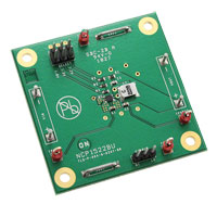
Figure 1. Board Picture in TSOP−5
© Semiconductor Components Industries, LLC, 2012
April, 2012 − Rev. 1
Figure 2. Board Picture in UDFN−6
1
Publication Order Number:
EVBUM2105/D
�NCP1522BUGEVB
MAXIMUM RATINGS (Note 1)
Rating
Symbol
Value
Unit
Vmin
−0.3
V
Vmax
7.0
V
Vmax
VIN + 0.3
V
Rqja
300
260
°C/W
Operating Ambient Temperature Range
TA
−40 to 85
°C
Storage Temperature Range
Tstg
−55 to 150
°C
Junction Operating Temperature
TJ
−40 to 125
°C
Lu
$100
mA
2.0
200
kV
V
1
per IPC
Minimum Voltage All Pins
Maximum Voltage All Pins (Note 2)
Maximum Voltage EN1, EN2, FB, LX
Thermal Resistance Junction to Air
TSOP−5
UDFN−6
Latchup Current Maximum Rating TA = 85°C (Note 4) Other Pins
ESD Withstand Voltage (Note 3)
Vesd
Human Body Model
Machine Model
Moisture Sensitivity Level (Note 5)
MSL
Stresses exceeding Maximum Ratings may damage the device. Maximum Ratings are stress ratings only. Functional operation above the
Recommended Operating Conditions is not implied. Extended exposure to stresses above the Recommended Operating Conditions may affect
device reliability.
1. Maximum electrical ratings are defined as those values beyond which damage to the device may occur at TA = 25°C
2. According JEDEC standard JESD22−A108B
3. This device series contains ESD protection and exceeds the following tests:
Human Body Model (HBM) per JEDEC standard: JESD22−A114
Machine Model (MM) per JEDEC standard: JESD22−A115
4. Latchup current maximum rating per JEDEC standard: JESD78.
5. JEDEC Standard: J−STD−020A.
ELECTRICAL CHARACTERISTICS
For Electrical Characteristic, please report to our NCP1522B datasheet available on our website, www.onsemi.com.
NCP1522B − BOARD CONNECTIONS
Symbol
Switch Descriptions
INPUT POWER
VIN+
This is the positive connection for power supply.
VIN−
This is the return connection for the power supply
GND1, GND2
Ground clip
SETUP
ENABLE
To enable the buck converter, connect a shorting jumper between ENABLE−1 and ENABLE−2.
To disable the buck converter, connect a shorting jumper between ENABLE−3 and ENABLE−2.
SELECT
A shorting jumper must be used to select an output voltage of 1.2V, 1.5V or 1.8V
OUTPUT POWER
VOUT+
This is the positive connection of the output voltage.
VOUT−
This is the return connection of the output voltage.
TEST POINT
TPVIN
This is the test point of the input voltage.
TPEN
This is the test point of the enable pin.
TPLX
This is the test point of the inductor voltage.
TPVOUT
This is the test point of the output voltage.
http://onsemi.com
2
�NCP1522BUGEVB
NCP1522B − BOARD SCHEMATIC
TPLX
TP3
TPVIN
TP1
CON2
1
2
VIN
U1
VIN
C1
4.7mF
VIN
1
VIN
2
EN
LX
5
SW
TPVOUT
TP4
L1
2.2mH
VOUT
GND
3
EN
FB
VOUT
1
2
R1
510k
4
C3
18pF
CON2
NCP1522
VIN
TPEN
TP2
1
2
3
SELECT
CON3x2
EN
H1
FIX
H2
FIX
H3
FIX
H4
FIX
1
1
1
1
2
2
C2
4.7mF
1.8V
1.5V
R4
250k
1
3
5
ENABLE
CON3x1
GND2
JMP2
R3
330k
2
4
6
GND1
JMP1
1
1
1.2V
R2
510k
Figure 3. Board Schematic in TSOP−5
FB
TPLX
TP3
U1
TPVIN
TP1
CON2
VIN
2
VIN
3
FB
GND
LX
VIN
GND
5
SW
TPVOUT
TP4
L1
2.2mH
VOUT
R1
510k
TPEN
TP2
SELECT
CON3x2
EN
C2
4.7mF
H1
FIX
H2
FIX
H3
FIX
H4
FIX
Figure 4. Board Schematic in UDFN−6
http://onsemi.com
3
1
1
1
2
2
2
4
6
1
2
3
VIN
R4
250k
CON2
1
3
5
ENABLE
CON3x1
R3
330k
1.5V
1.2V
1
1
GND2
JMP2
C3
18pF
FB
R2
510k
GND1
JMP1
VOUT
1
2
4
NCP1522U
C1
4.7mF
VIN
EN
6
1
1
2
1
1.8V
EN
�NCP1522BUGEVB
NCP1522B − TEST PROCEDURE
Equipment needed
4. Connect the power supply connector to connectors
VIN+ and VIN−. The DC current measurement on
VIN line should be around 0.3 mA.
5. Close ENABLE connector. The DC current
measurement on Vin line should be around 55 mA.
6. Measure the output voltage between VOUT+ and
VOUT− connectors. You should see around 1.2 V
voltage operation.
7. Remove the ENABLE jumper. The DC current
measurement on Vin line should be back around
0.3 mA.
• Power supply
• Digital Volt Meter
• Digital Amp Meter
Test
1. Jumper ENABLE should be open.
2. Jumper SELECT should be closed to 1.2 V.
3. Set the power supply to 3.6 V and the current limit
of at least 800 mA.
NCP1522B − BILL OF MATERIAL
Footprint
Manufacturer
Manufacturer
Part Number
Designator
Qty.
Description
Value
Tolerance
U1
1
IC, Converter,
DC/DC
NA
NA
TSOP−5
UDFN
ON Semiconductor
NCP1522B
NCP1522BU
C1
1
Ceramic
capacitor
4.7mF, 10V,
X5R
10%
0805
TDK
C1608X5R1A475
C2
1
Ceramic
capacitor
10mF, 6.3V,
X5R
10%
0603
TDK
C1608X5R0J105
C3
1
Ceramic
capacitor
18pF, 50V,
COG
5%
0603
TDK
C1608C0G1H180
R1, R2
2
SMD resistor
510k
1%
0603
std
std
R3
1
SMD resistor
330k
1%
0603
std
std
R4
1
SMD resistor
240k
1%
0603
std
std
L1
1
Inductor
2,2mH
30%
1210
Coilcraft
LPS3008−222NL
VIN, VOUT
4
Connector
NA
NA
NA
Kontek Comatel
Cambion
3110014000500
160−1724−02−05−00
ENABLE
1
3 Pin Jumper
Header
NA
NA
2,54mm
TYCO/AMP
Molex / Waldom
5−826629−0
90120−0160
SELECT
1
3x2 Pin Jumper
Header
NA
NA
2,54mm
TYCO/AMP
Molex / Waldom
4731955180470
90131−0140
GND1,
GND2
2
Jumper for GND
NA
NA
10,16mm
Harwin
Molex / Waldom
D3082−01
90120−0160
TPEN,
TPLX,
TPVIN,
TPVOUT
4
Test Point
Type 3
NA
NA
f1,60mm
Keystone
5010
PCB
1
50.8mm x
50.8mm x 1mm,
4 Layers
NA
NA
NA
Any
TLS−P−004−A−1106−BR
TLS−P−003−A−0207−BR
http://onsemi.com
4
�NCP1522BUGEVB
NCP1522B − PCB LAYOUT
Board reference: TLS−P−001−A−0107−BR
Board reference: TLS−P−001−A−0207−BR
Figure 5. Assembly Layer in TSOP−5
Figure 6. Assembly Layer in UDFN−6
Figure 7. Part Layout in TSOP−5
Figure 8. Part Layout in UDFN−6
http://onsemi.com
5
�NCP1522BUGEVB
Figure 9. Top Layer Routing in TSOP−5
Figure 10. Top Layer Routing in UDFN−6
Figure 11. Ground Layer Routing in UDFN−6
Figure 12. Ground Layer Routing in UDFN−6
http://onsemi.com
6
�NCP1522BUGEVB
Figure 13. Power Layer Routing in TSOP−5
Figure 14. Power Layer Routing in UDFN−6
Figure 15. Bottom Layer Routing in TSOP−5
Figure 16. Bottom Layer Routing in UDFN−6
http://onsemi.com
7
�onsemi,
, and other names, marks, and brands are registered and/or common law trademarks of Semiconductor Components Industries, LLC dba “onsemi” or its affiliates
and/or subsidiaries in the United States and/or other countries. onsemi owns the rights to a number of patents, trademarks, copyrights, trade secrets, and other intellectual property. A
listing of onsemi’s product/patent coverage may be accessed at www.onsemi.com/site/pdf/Patent−Marking.pdf. onsemi is an Equal Opportunity/Affirmative Action Employer. This
literature is subject to all applicable copyright laws and is not for resale in any manner.
The evaluation board/kit (research and development board/kit) (hereinafter the “board”) is not a finished product and is not available for sale to consumers. The board is only intended
for research, development, demonstration and evaluation purposes and will only be used in laboratory/development areas by persons with an engineering/technical training and familiar
with the risks associated with handling electrical/mechanical components, systems and subsystems. This person assumes full responsibility/liability for proper and safe handling. Any
other use, resale or redistribution for any other purpose is strictly prohibited.
THE BOARD IS PROVIDED BY ONSEMI TO YOU “AS IS” AND WITHOUT ANY REPRESENTATIONS OR WARRANTIES WHATSOEVER. WITHOUT LIMITING THE FOREGOING,
ONSEMI (AND ITS LICENSORS/SUPPLIERS) HEREBY DISCLAIMS ANY AND ALL REPRESENTATIONS AND WARRANTIES IN RELATION TO THE BOARD, ANY
MODIFICATIONS, OR THIS AGREEMENT, WHETHER EXPRESS, IMPLIED, STATUTORY OR OTHERWISE, INCLUDING WITHOUT LIMITATION ANY AND ALL
REPRESENTATIONS AND WARRANTIES OF MERCHANTABILITY, FITNESS FOR A PARTICULAR PURPOSE, TITLE, NON−INFRINGEMENT, AND THOSE ARISING FROM A
COURSE OF DEALING, TRADE USAGE, TRADE CUSTOM OR TRADE PRACTICE.
onsemi reserves the right to make changes without further notice to any board.
You are responsible for determining whether the board will be suitable for your intended use or application or will achieve your intended results. Prior to using or distributing any systems
that have been evaluated, designed or tested using the board, you agree to test and validate your design to confirm the functionality for your application. Any technical, applications or
design information or advice, quality characterization, reliability data or other services provided by onsemi shall not constitute any representation or warranty by onsemi, and no additional
obligations or liabilities shall arise from onsemi having provided such information or services.
onsemi products including the boards are not designed, intended, or authorized for use in life support systems, or any FDA Class 3 medical devices or medical devices with a similar
or equivalent classification in a foreign jurisdiction, or any devices intended for implantation in the human body. You agree to indemnify, defend and hold harmless onsemi, its directors,
officers, employees, representatives, agents, subsidiaries, affiliates, distributors, and assigns, against any and all liabilities, losses, costs, damages, judgments, and expenses, arising
out of any claim, demand, investigation, lawsuit, regulatory action or cause of action arising out of or associated with any unauthorized use, even if such claim alleges that onsemi was
negligent regarding the design or manufacture of any products and/or the board.
This evaluation board/kit does not fall within the scope of the European Union directives regarding electromagnetic compatibility, restricted substances (RoHS), recycling (WEEE), FCC,
CE or UL, and may not meet the technical requirements of these or other related directives.
FCC WARNING – This evaluation board/kit is intended for use for engineering development, demonstration, or evaluation purposes only and is not considered by onsemi to be a finished
end product fit for general consumer use. It may generate, use, or radiate radio frequency energy and has not been tested for compliance with the limits of computing devices pursuant
to part 15 of FCC rules, which are designed to provide reasonable protection against radio frequency interference. Operation of this equipment may cause interference with radio
communications, in which case the user shall be responsible, at its expense, to take whatever measures may be required to correct this interference.
onsemi does not convey any license under its patent rights nor the rights of others.
LIMITATIONS OF LIABILITY: onsemi shall not be liable for any special, consequential, incidental, indirect or punitive damages, including, but not limited to the costs of requalification,
delay, loss of profits or goodwill, arising out of or in connection with the board, even if onsemi is advised of the possibility of such damages. In no event shall onsemi’s aggregate liability
from any obligation arising out of or in connection with the board, under any theory of liability, exceed the purchase price paid for the board, if any.
The board is provided to you subject to the license and other terms per onsemi’s standard terms and conditions of sale. For more information and documentation, please visit
www.onsemi.com.
PUBLICATION ORDERING INFORMATION
LITERATURE FULFILLMENT:
Email Requests to: orderlit@onsemi.com
onsemi Website: www.onsemi.com
◊
TECHNICAL SUPPORT
North American Technical Support:
Voice Mail: 1 800−282−9855 Toll Free USA/Canada
Phone: 011 421 33 790 2910
www.onsemi.com
1
Europe, Middle East and Africa Technical Support:
Phone: 00421 33 790 2910
For additional information, please contact your local Sales Representative
�