NCP1522B
Buck Converter - DC-DC
3 MHz, 600 mA
The NCP1522B step−down DC−DC converter is a monolithic
integrated circuit optimized for portable applications powered from one
cell Li−Ion or three cell Alkaline/NiCd/NiMH batteries. The part,
available in adjustable output voltage versions ranging from 0.9 V to
3.3 V, is able to deliver up to 600 mA. It uses synchronous rectification
to increase efficiency and reduce external part count. The device also
has a built−in 3 MHz (nominal) oscillator which reduces component
size by allowing smaller inductors and capacitors. Automatic switching
PWM/PFM mode offers improved system efficiency.
Additional features include integrated soft−start, cycle−by−cycle
current limiting and thermal shutdown protection. The NCP1522B is
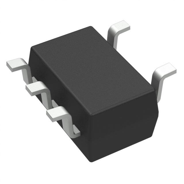
available in a space saving, low profile TSOP5 and UDFN6 packages.
Up to 93% Efficiency
Allow Use of Small External Components
Source up to 600 mA
3 MHz Switching Frequency
Adjustable Output Voltage from 0.9 V to 3.3 V
Synchronous Rectification for Higher Efficiency
2.7 V to 5.5 V Input Voltage Range
Low Quiescent Current
Shutdown Current Consumption of 0.3 mA
Thermal Limit Protection
Short Circuit Protection
All Pins are Fully ESD Protected
These are Pb−Free Devices
1
1
VIN
LX
5
2
GND
3
EN
L
OFF ON
COUT
FB
1
1
2
3
6
BRMG 5
G
4
Shipping†
Package
NCP1522BSNT1G
TSOP−5 3000/Tape & Reel
(Pb−Free)
NCP1522BMUTBG
UDFN6 3000/Tape & Reel
(Pb−Free)
†For information on tape and reel specifications,
including part orientation and tape sizes, please
refer to our Tape and Reel Packaging Specification
Brochure, BRD8011/D.
R2
VOUT
R1
GANAYWG
G
ORDERING INFORMATION
Device
CIN
OFF ON
5
BR
= Specific Device Code
M
= Date Code
G
= Pb−Free Package
(Note: Microdot may be in either location)
Cellular Phones, Smart Phones and PDAs
Digital Still/Video Cameras
MP3 Players and Portable Audio Systems
Wireless and DSL Modems
Portable Equipment
USB Powered Devices
VIN
5
TSOP−5
SN SUFFIX
CASE 483
UDFN6
MU SUFFIX
CASE 517AB
Typical Applications
•
•
•
•
•
•
MARKING
DIAGRAM
GAN
= Specific Device Code
A
= Assembly Location
Y
= Year
W
= Work Week
G
= Pb−Free Package
(Note: Microdot may be in either location)
Features
•
•
•
•
•
•
•
•
•
•
•
•
•
http://onsemi.com
Cff
4
1 EN
FB
6
2 GND LX
5
3 VIN GND
4
L
R1
Cff
VOUT
COUT
R2
VIN
Figure 1. Typical Application − TSOP−5
© Semiconductor Components Industries, LLC, 2010
August, 2019 − Rev. 1
1
CIN
Figure 2. Typical Application − UDFN6
Publication Order Number:
NCP1521B/D
�NCP1522B
100
95
EFFICIENCY (%)
90
85
80
75
70
65
VOUT = 3.3 V
VIN = 4.2 V
TA = 25°C
60
55
50
0
100
200
300
400
500
600
IOUT, OUTPUT CURRENT (mA)
Figure 3. Efficiency vs. Output Current
Q1
Vbattery
Q2
VIN
1
LX
5
PWM/PFM
CONTROL
2.2 mH
4.7 mF
4.7 mF
GND
2
Enable
EN
3
R1
ILIMIT
LOGIC
CONTROL
& THERMAL
SHUTDOWN
FB
4
REFERENCE
VOLTAGE
R2
Figure 4. Simplified Block Diagram
http://onsemi.com
2
18 pF
�NCP1522B
PIN FUNCTION DESCRIPTION
Pin
TSOP−5
Pin
UDFN6
Pin Name
Type
1
3
VIN
Analog /
Power Input
Power supply input for the PFET power stage, analog and digital blocks. The
pin must be decoupled to ground by a 10 mF ceramic capacitor.
2
2, 4
GND
Analog /
Power Ground
This pin is the GND reference for the NFET power stage and the analog section of the IC. The pin must be connected to the system ground.
3
1
EN
Digital Input
Enable for switching regulators. This pin is active HIGH and is turned off by
logic LOW on this pin.
4
6
FB
Analog Input
Feedback voltage from the output of the power supply. This is the input to the
error amplifier.
5
5
LX
Analog Output
Description
Connection from power MOSFETs to the Inductor.
PIN CONNECTIONS
VIN
1
GND
2
EN
3
5
4
LX
FB
EN
1
6
FB
GND
2
5
LX
VIN
3
4
GND
(Top View)
Figure 5. Pin Connections − TSOP−5
Figure 6. Pin Connections − UDFN6
MAXIMUM RATINGS
Rating
Symbol
Value
Unit
Minimum Voltage All Pins
Vmin
−0.3
V
Maximum Voltage All Pins (Note 2)
Vmax
7.0
V
Maximum Voltage EN, FB, LX
Vmax
VIN + 0.3
V
Thermal Resistance, Junction−to−Air
(with Recommended Soldering Footprint)
TSOP−5
UDFN6
RqJA
300
260
°C/W
Operating Ambient Temperature Range
TA
−40 to 85
°C
Storage Temperature Range
Tstg
−55 to 150
°C
Junction Operating Temperature
Tj
−40 to 125
°C
Latchup Current Maximum Rating (TA = 85°C) (Note 4) Other Pins
Lu
$100
mA
2.0
200
kV
V
1
per IPC
ESD Withstand Voltage (Note 3)
Human Body Model
Machine Model
Vesd
Moisture Sensitivity Level (Note 5)
MSL
Stresses exceeding Maximum Ratings may damage the device. Maximum Ratings are stress ratings only. Functional operation above the
Recommended Operating Conditions is not implied. Extended exposure to stresses above the Recommended Operating Conditions may affect
device reliability.
1. Maximum electrical ratings are defined as those values beyond which damage to the device may occur at TA = 25°C.
2. According to JEDEC standard JESD22−A108B.
3. This device series contains ESD protection and exceeds the following tests:
Human Body Model (HBM) per JEDEC standard: JESD22−A114.
Machine Model (MM) per JEDEC standard: JESD22−A115.
4. Latchup current maximum rating per JEDEC standard: JESD78.
5. JEDEC Standard: J−STD−020A.
http://onsemi.com
3
�NCP1522B
ELECTRICAL CHARACTERISTICS (Typical values are referenced to TA = +25°C, Min and Max values are referenced −40°C to +85°C
ambient temperature, unless otherwise noted, operating conditions VIN = 3.6 V, VOUT = 1.2 V, unless otherwise noted.)
Pin
Rating
TSOP
UDFN
Symbol
Min
Typ
Max
Unit
VIN PIN
Input Voltage Range
1
3
VIN
2.7
−
5.5
V
Quiescent Current, PFM No Switching
1
3
Iq ON
−
50
90
mA
Standby Current, EN Low
1
3
Iq OFF
−
0.2
1.5
mA
Under Voltage Lockout (VIN Falling)
1
3
VUVLO
2.2
2.4
2.55
V
Positive Going Input High Voltage Threshold, EN0 Signal
3
1
VIH
1.2
−
−
V
Negative Going Input High Voltage Threshold, EN0 Signal
3
1
VIL
−
−
0.4
V
EN High Input Current, EN = 3.6 V
3
1
IENH
−
2.0
−
mA
−
−3.0
$1.0
$2.0
−
$3.0
EN PIN
OUTPUT
%
Output Voltage Accuracy (Note 6)
Ambient Temperature
Overtemperature Range
DVOUT
Minimum Output Voltage (Note 7)
VOUT
−
0.9
−
V
Maximum Output Voltage
VOUT
−
3.3
−
V
Output Voltage Load Regulation Overtemperature
IOUT = 100 mA to 600 mA
VOUT
−
0.0008
−
Load Transient Response, Rise/Falltime 1 ms
10 mA to 100 mA Load Step
200 mA to 600 mA Load Step
VOUT
−
−
50
54
−
−
Output Voltage Line Regulation, IOUT = 100 mA,
VIN = 2.7 V to 5.5 V
VOUT
−
0.08
−
Line Transient Response, IOUT = 100 mA,
3.6 V to 3.0 V Line Step (Falltime=50 ms)
VOUT
−
2.0
−
Output Voltage Ripple, IOUT = 300 mA (PWM Mode)
VOUT
−
1.0
−
mV
Output Voltage Ripple, IOUT = 0 mA (PFM Mode)
VOUT
−
8.0
−
mV
%/mA
mV
%
mVPP
Peak Inductor Current
5
5
ILIM
−
1200
−
mA
Oscillator Frequency
5
5
FOSC
2.4
3.0
3.6
MHz
Duty Cycle
5
5
−
−
−
100
%
Soft−Start Time
TSTART
−
320
500
ms
Thermal Shutdown Threshold
TSD
−
160
−
°C
Thermal Shutdown Hysteresis
TSDH
−
25
−
°C
P−Channel On−Resistance
RLxH
−
400
−
mW
N−Channel On−Resistance
RLxL
−
400
−
mW
P−Channel Leakage Current
ILeakH
−
0.05
−
mA
N−Channel Leakage Current
ILeakL
−
0.01
−
mA
POWER SWITCHES
6. The overall output voltage tolerance depends upon the accuracy of the external resistor (R1, R2).
7. For VOUT = 0.9 V, maximum input voltage do not exceed 5.2 V.
http://onsemi.com
4
�NCP1522B
TABLE OF GRAPHS
Typical Characteristics for Step−down Converter
ISTB
Standby Current
vs. Input Voltage
7
Quiescent Current, PFM No Switching
vs. Input Voltage
8
Output Voltage Accuracy
vs. Temperature
9, 10
Efficiency
vs. Output Current
Freq
Switching Frequency
vs. Input Voltage
14
VOUT
Soft−Start
vs. Time
15
VOUT
Short Circuit Protection
vs. Time
16
VOUT
Line Regulation
vs. Input Voltage
17, 18
VOUT
Line Transient
vs. Time
19, 20
VOUT
Load Regulation
vs. Output Current
21, 22
VOUT
Load Transient
vs. Time
Iq
VOUT
Eff
0.9
QUIESCENT CURRENT (mA)
0.7
0.6
0.5
0.4
0.3
0.2
0.1
0
11, 12, 13
23, 24, 25, 26
56
0.8
STANDBY CURRENT (mA)
Figure
2.5
3.0
3.5
4.0
4.5
5.0
5.5
54
52
50
48
46
44
2.5
VIN, INPUT VOLTAGE (V)
3.0
3.5
4.0
4.5
VIN, INPUT VOLTAGE (V)
Figure 7. Shutdown Current vs. Supply Voltage
5.0
5.5
Figure 8. Quiescent Current PFM No Switching
vs. Supply Voltage
http://onsemi.com
5
�NCP1522B
3.0
3.0
2.0
IOUT = 600 mA
1.0
ACCURACY (%)
ACCURACY (%)
2.0
IOUT = 20 mA
IOUT = 200 mA
0
−1.0
−2.0
−3.0
0
1.0
VIN = 3.6 V
VIN = 2.7 V
0
VIN = 5.5 V
−1.0
−2.0
−3.0
20
40
60
80
TEMPERATURE (°C)
100
120
0
20
40
60
80
TEMPERATURE (°C)
100
120
Figure 9. Output Voltage Accuracy vs. Temperature
(VIN = 3.6 V, VOUT = 1.2 V)
Figure 10. Output Voltage Accuracy vs. Temperature
(VOUT = 1.2 V, IOUT = 200 mA)
100
100
95
95
90
EFFICIENCY (%)
EFFICIENCY (%)
90
VOUT = 3.3 V
85
VOUT = 1.8 V
80
75
VOUT = 0.9 V
70
65
80
65
55
55
200
300
400
500
50
600
VIN = 2.7 V
70
60
100
VIN = 5.5 V
75
60
50
0
VIN = 3.6 V
85
0
100
200
300
400
500
IOUT, OUTPUT CURRENT (mA)
IOUT, OUTPUT CURRENT (mA)
Figure 11. Efficiency vs. Output Current
(VIN = 3.6 V, TA = 255C)
Figure 12. Efficiency vs. Output Current
(VOUT = 1.2 V, TA = 255C)
100
600
3.6
95
3.4
85
FREQUENCY (MHz)
EFFICIENCY (%)
90
−40°C
80
75
25°C
70
85°C
65
60
−40°C
3
2.8
25°C
85°C
2.6
55
50
3.2
0
100
200
300
400
500
IOUT, OUTPUT CURRENT (mA)
2.4
2.5
600
Figure 13. Efficiency vs. Output Current
(VIN = 3.6 V, VOUT = 1.2 V)
3
3.5
4
4.5
VIN, INPUT VOLTAGE (V)
5
Figure 14. Switching Frequency vs. Input
Voltage (VOUT = 1.2 V, IOUT = 300 mA)
http://onsemi.com
6
5.5
�NCP1522B
VIN
2 V/div
VOUT
500 mV/div
ILX
500 mV/div
ILX
100 mV/div
Time
100 ms/div
Time
10 ms/div
Figure 16. Short−Circuit Protection
(VIN = 3.6 V, VOUT = 1.2 V)
1
1
0.8
0.8
0.6
0.6
85°C
0.2
LINE REGULATION (%)
LINE REGULATION (%)
Figure 15. Typical Soft−Start
(VOUT = 1.2 V, IOUT = 250 mA)
0.4
25°C
0
−0.2
−40°C
−0.4
VOUT
200 mV/div
−0.6
IOUT = 1 mA
0.4
IOUT = 600 mA
0.2
0
−0.2
IOUT = 300 mA
−0.4
−0.6
−0.8
−0.8
−1
2.7
3.2
3.7
4.2
4.7
−1
2.7
5.2
VIN, INPUT VOLTAGE (V)
3.2
3.7
4.2
4.7
5.2
VIN, INPUT VOLTAGE (V)
Figure 17. Line Regulation
(VOUT = 1.2 V, IOUT = 300 mA)
Figure 18. Line Regulation
(VOUT = 1.2 V, TA = 255C)
VIN
0.5 V/div
VIN
0.5 V/div
VOUT
20 mV/div
VOUT
20 mV/div
Figure 19. 3.0 V to 3.6 V Line Transient
(Risetime = 50 ms, VOUT = 1.2 V, IOUT = 100 mA,
TA = 255C)
Figure 20. 3.6 V to 3.0 V Line Transient
(Risetime = 50 ms, VOUT = 1.2 V, IOUT = 100 mA,
TA = 255C)
http://onsemi.com
7
�3.0
3.0
2.0
2.0
LOAD REGULATION (%)
LOAD REGULATION (%)
NCP1522B
−40°C
1.0
0.0
−1.0
25°C
−2.0
−3.0
0
VIN = 5.5 V
1.0
VIN = 3.6 V
0.0
−1.0
VIN = 2.7 V
−2.0
85°C
−3.0
100
200
300
400
500
IOUT, OUTPUT CURRENT (mA)
0
600
Figure 21. Load Regulation
(VIN = 3.6 V, VOUT = 1.2 V)
100
200
300
400
500
IOUT, OUTPUT CURRENT (mA)
Figure 22. Load Regulation
(VOUT = 1.2 V, TA = 255C)
IOUT
50 mA/div
VOUT
20 mV/div
VOUT
20 mV/div
IOUT
20 mA/div
Figure 24. 100 mA to 10 mA Load Transient
(VIN = 3.6 V, VOUT = 1.2 V, TA = 255C)
Figure 23. 10 mA to 100 mA Load Transient
(VIN = 3.6 V, VOUT = 1.2 V, TA = 255C)
VOUT
20 mV/div
VOUT
20 mV/div
IOUT
200 mA/div
IOUT
200 mA/div
Figure 26. 600 mA to 200 mA Load Transient
(VIN = 3.6 V, VOUT = 1.2 V, TA = 255C)
Figure 25. 200 mA to 600 mA Load Transient
(VIN = 3.6 V, VOUT = 1.2 V, TA = 255C)
http://onsemi.com
8
600
�NCP1522B
DC/DC OPERATION DESCRIPTION
Detailed Description
The NCP1522B uses a constant frequency, voltage mode
step−down architecture. Both the main (P−Channel
MOSFET) and synchronous (N−Channel MOSFET)
switches are internal.
The output voltage is set by an external resistor divider
in the range of 0.9 V to 3.3 V and can source at least
600 mA.
The NCP1522B works with two modes of operation;
PWM/PFM depending on the current required. In PWM
mode, the device can supply voltage with a tolerance of
"3% and 90% efficiency or better. Lighter load currents
cause the device to automatically switch into PFM mode to
reduce current consumption and extended battery life.
Additional features include soft−start, undervoltage
protection, current overload protection, and thermal
shutdown protection. As shown in Figure 1, only six
external components are required. The part uses an internal
reference voltage of 0.6 V. It is recommended to keep
NCP1522B in shutdown mode until the input voltage is
2.7 V or higher.
VOUT 10 mV/div
ILx 100 mA/div
VLx 2 V/div
200 ns/div
Figure 27. PWM Switching Waveform
(VIN = 3.6 V, VOUT = 1.2 V, IOUT = 600 mA)
PFM Operating Mode
Under light load conditions, the NCP1522B enters in low
current PFM mode operation to reduce power
consumption. The output regulation is implemented by
pulse frequency modulation. If the output voltage drops
below the threshold of PFM comparator, a new cycle will
be initiated by the PFM comparator to turn on the switch
Q1. Q1 remains ON during the minimum on time of the
structure while Q2 is in its current source mode. The peak
inductor current depends upon the drop between input and
output voltage. After a short dead time delay where Q1 is
switched OFF, Q2 is turned in its ON state. The negative
current detector will detect when the inductor current drops
below zero and sends the signal to turn Q2 to current source
mode to prevent a too large deregulation of the output
voltage. When the output voltage falls below the threshold
of the PFM comparator, a new cycle starts immediately.
PWM Operating Mode
In this mode, the output voltage of the device is regulated
by modulating the on−time pulse width of the main switch
Q1 at a fixed 3 MHz frequency.
The switching of the PMOS Q1 is controlled by a
flip−flop driven by the internal oscillator and a comparator
that compares the error signal from an error amplifier with
the sum of the sensed current signal and compensation
ramp.
The driver switches ON and OFF the upper side transistor
(Q1) and switches the lower side transistor in either ON
state or in current source mode.
At the beginning of each cycle, the main switch Q1 is
turned ON by the rising edge of the internal oscillator
clock. The inductor current ramps up until the sum of the
current sense signal and compensation ramp becomes
higher than the error amplifier’s voltage. Once this has
occurred, the PWM comparator resets the flip−flop, Q1 is
turned OFF while the synchronous switch Q2 is turned in
its current source mode. Q2 replaces the external Schottky
diode to reduce the conduction loss and improve the
efficiency. To avoid overall power loss, a certain amount of
dead time is introduced to ensure Q1 is completely turned
OFF before Q2 is being turned ON.
Vout
VLx
Figure 28. PFM Switching Waveforms
(VIN = 3.6 V, VOUT = 1.2 V, IOUT = 0 mA, Temp = 25_C)
http://onsemi.com
9
�NCP1522B
Soft−Start
Undervoltage Lockout
The NCP1522B uses soft−start to limit the inrush current
when the device is initially powered up or enabled.
Soft−start is implemented by gradually increasing the
reference voltage until it reaches the full reference voltage.
During startup, a pulsed current source charges the internal
soft−start capacitor to provide gradually increasing
reference voltage. When the voltage across the capacitor
ramps up to the nominal reference voltage, the pulsed
current source will be switched off and the reference
voltage will switch to the regular reference voltage.
The input voltage VIN must reach 2.4 V (typ) before the
NCP1522B enables the DC/DC converter output to begin
the start up sequence (see Soft−Start section). The UVLO
threshold hysteresis is typically 100 mV.
Shutdown Mode
Forcing this pin to a voltage below 0.4 V will shut down
the IC. In shutdown mode, the internal reference, oscillator
and most of the control circuitries are turned off. Therefore,
the typical current consumption will be 0.3 mA (typical
value). Applying a voltage above 1.2 V to EN pin will
enable the device for normal operation. The typical
threshold is around 0.7 V. The device will go through
soft−start to normal operation.
Cycle−by−Cycle Current Limitation
From the block diagram, an ILIM comparator is used to
realize cycle−by−cycle current limit protection. The
comparator compares the LX pin voltage with the
reference voltage, which is biased by a constant current. If
the inductor current reaches the limit, the ILIM comparator
detects the LX voltage falling below the reference voltage
and releases the signal to turn off the switch Q1. The
cycle−by−cycle current limit is set at 1200 mA (nom).
Thermal Shutdown
Internal Thermal Shutdown circuitry is provided to
protect the integrated circuit in the event that the maximum
junction temperature is exceeded. If the junction
temperature exceeds 160°C, the device shuts down. In this
mode switch Q1 and Q2 and the control circuits are all
turned off. The device restarts in soft−start after the
temperature drops below 135°C. This feature is provided
to prevent catastrophic failures from accidental device
overheating, and it is not intended as a substitute for proper
heatsinking.
Low Dropout Operation
The NCP1522B offers a low input to output voltage
difference. The NCP1522B can operate at 100% duty
cycle. In this mode the PMOS (Q1) remains completely on.
The minimum input voltage to maintain regulation can
be calculated as:
Short Circuit Protection
VIN(min) + VOUT(max)
) (IOUT (RDS(ON) ) RINDUCTOR))
When the output is shorted to ground, the device limits
the inductor current. The duty−cycle is minimum and the
consumption on the input line is 300 mA (Typ). When the
short circuit condition is removed, the device returns to the
normal mode of operation.
(eq. 1)
•
•
•
•
VOUT: Output Voltage (Volts)
IOUT: Max Output Current
RDS(ON) = P−Channel Switch RDS(ON)
RINDUCTOR: Inductor Resistance (DCR)
http://onsemi.com
10
�NCP1522B
APPLICATION INFORMATION
Output Voltage Selection
The corner frequency is given by:
The output voltage is programmed through an external
resistor divider connected from VOUT to FB then to GND.
For low power consumption and noise immunity, the
resistor from FB to GND (R2) should be in the
[100 k−600 k] range. If R2 is 200 k given the VFB is 0.6 V,
the current through the divider will be 3.0 mA.
The formula below gives the value of VOUT, given the
desired R1 and the R1 value:
VOUT + VFB
•
•
•
•
(1 ) R1)
R2
fc +
2p ǸL
(eq. 2)
Inductance (L)
In PWM operating mode, the input current is pulsating
with a large switching noise. Using an input bypass
capacitor can reduce the peak current transients drawn
from
the
input supply source, thereby reducing switching noise
significantly. The capacitance needed for the input bypass
capacitor depends on the source impedance of the input
supply.
The maximum RMS current occurs at 50% duty cycle
with maximum output current, which is Iout_max/2.
For NCP1522B, a low profile ceramic capacitor of
4.7 mF should be used for most of the cases. For effective
bypass results, the input capacitor should be placed as close
as possible to the VIN pin.
Taiyo Yuden
TDK
JMK212BY475MG
C2012X5ROJ475KB
C1632X5ROJ475KT
1
2p Ǹ2.2 mH
4.7 mF
+ 49 kHz
(eq. 3)
Output Capacitor (COUT)
1.0
mH
10
mF
2.2
mH
4.7
mF
Inductor Selection
The inductor parameters directly related to device
performances are saturation current and DC resistance and
inductance value. The inductor ripple current (DIL)
decreases with higher inductance:
ǒ
V
V
DIL + OUT 1− OUT
L fSW
VIN
Ǔ
(eq. 4)
• DIL: Peak to Peak Inductor Ripple Current
• L: Inductor Value
• fSW: Switching Frequency
The saturation current of the inductor should be rated
higher than the maximum load current plus half the ripple
current:
Table 1. List of Input Capacitors
GRM21BR71C475KA
+
Table 2. L−C Filter Example
Input Capacitor Selection
Murata
COUT
The device is intended to operate with inductance value
of 2.2 mH.
If the corner frequency is moved, it is recommended to
check the loop stability depending on the accepted output
ripple voltage and the required output curret. Take care to
check the loop stability. The phase margin is usually higher
than 45°.
VOUT: Output Voltage (Volts)
VFB: Feedback Voltage = 0.6 V
R1: Feedback Resistor from VOUT to FB
R2: Feedback Resistor from FB to GND
GRM188R60J475KE
1
DI
IL(MAX) + IO(MAX) ) L
2
4.7 mF
• DIL(MAX): Maximum Inductor Current
• DIO(MAX): Maximum Output Current
4.7 mF
(eq. 5)
The inductor’s resistance will factor into the overall
efficiency of the converter. For best performance, the DC
resistance should be less than 0.3 W for good efficiency.
4.7 mF
Output L−C Filter Design Considerations
The NCP1522B operates at 3 MHz frequency and uses
voltage mode architecture. The correct selection of the
output filter ensures good stability and fast transient
response.
Due to the nature of the buck converter, the output L−C
filter must be selected to work with internal compensation.
For NCP1522B, the internal compensation is internally
fixed and it is optimized for an output filter of L = 2.2 mH
and COUT = 4.7 mF.
Table 3. LIST OFINDUCTORS
Coilcraft
LPO3010 Series
FDK
MIPW3226 Series
TDK
VLF3010AT Series
Taiyo Yuden
LQ CBL2012 Series
http://onsemi.com
11
DO1605−T Series
�NCP1522B
Output Capacitor Selection
Table 4. LIST OF OUTPUT CAPACITORS
Selecting the proper output capacitor is based on the
desired output ripple voltage. Ceramic capacitors with low
ESR values will have the lowest output ripple voltage and
are strongly recommended. The output capacitor requires
an X7R dielectric.
The output ripple voltage in PWM mode is given by:
DVOUT + DIL
•
•
•
•
•
ǒ4
Ǔ
1
) ESR
fSW COUT
GRM188R60J475KE
Murata
GRM21BR71C475KA
GRM188R60OJ106ME
GRM21BR60J106ME19L
Taiyo Yuden
(eq. 6)
TDK
10 mF
JMK212BY475MG
4.7 mF
JMK212BJ106MG
10 mF
C2012X5ROJ475KB
DVOUT: Output Voltage Ripple in PWM Mode
DIL: Peak to Peak Inductor Ripple Current
fSW: Switching Frequency
COUT: Output Capacitor
ESR: Output Capacitor Serial Resistor
4.7 mF
C1632X5ROJR75KT
C2012X5ROJ106K
4.7 mF
10 mF
Feed−Forward Capacitor Selection
The feed−forward capacitor sets the feedback loop
response and is critical to obtain good loop stability.
Given that the compensation is internally fixed, an 18 pF
or higher ceramic capacitor is needed. Choose a small
ceramic capacitor X7R dielectric.
http://onsemi.com
12
�MECHANICAL CASE OUTLINE
PACKAGE DIMENSIONS
TSOP−5
CASE 483
ISSUE N
5
1
SCALE 2:1
NOTES:
1. DIMENSIONING AND TOLERANCING PER ASME
Y14.5M, 1994.
2. CONTROLLING DIMENSION: MILLIMETERS.
3. MAXIMUM LEAD THICKNESS INCLUDES LEAD FINISH
THICKNESS. MINIMUM LEAD THICKNESS IS THE
MINIMUM THICKNESS OF BASE MATERIAL.
4. DIMENSIONS A AND B DO NOT INCLUDE MOLD
FLASH, PROTRUSIONS, OR GATE BURRS. MOLD
FLASH, PROTRUSIONS, OR GATE BURRS SHALL NOT
EXCEED 0.15 PER SIDE. DIMENSION A.
5. OPTIONAL CONSTRUCTION: AN ADDITIONAL
TRIMMED LEAD IS ALLOWED IN THIS LOCATION.
TRIMMED LEAD NOT TO EXTEND MORE THAN 0.2
FROM BODY.
D 5X
NOTE 5
2X
DATE 12 AUG 2020
0.20 C A B
0.10 T
M
2X
0.20 T
5
B
1
4
2
B
S
3
K
DETAIL Z
G
A
A
TOP VIEW
DIM
A
B
C
D
G
H
J
K
M
S
DETAIL Z
J
C
0.05
H
C
SIDE VIEW
SEATING
PLANE
END VIEW
GENERIC
MARKING DIAGRAM*
SOLDERING FOOTPRINT*
0.95
0.037
MILLIMETERS
MIN
MAX
2.85
3.15
1.35
1.65
0.90
1.10
0.25
0.50
0.95 BSC
0.01
0.10
0.10
0.26
0.20
0.60
0_
10 _
2.50
3.00
1.9
0.074
5
5
XXXAYWG
G
1
1
Analog
2.4
0.094
XXX = Specific Device Code
A
= Assembly Location
Y
= Year
W = Work Week
G
= Pb−Free Package
1.0
0.039
XXX MG
G
Discrete/Logic
XXX = Specific Device Code
M = Date Code
G
= Pb−Free Package
(Note: Microdot may be in either location)
0.7
0.028
SCALE 10:1
mm Ǔ
ǒinches
*For additional information on our Pb−Free strategy and soldering
details, please download the ON Semiconductor Soldering and
Mounting Techniques Reference Manual, SOLDERRM/D.
DOCUMENT NUMBER:
DESCRIPTION:
98ARB18753C
TSOP−5
*This information is generic. Please refer to
device data sheet for actual part marking.
Pb−Free indicator, “G” or microdot “ G”,
may or may not be present.
Electronic versions are uncontrolled except when accessed directly from the Document Repository.
Printed versions are uncontrolled except when stamped “CONTROLLED COPY” in red.
PAGE 1 OF 1
ON Semiconductor and
are trademarks of Semiconductor Components Industries, LLC dba ON Semiconductor or its subsidiaries in the United States and/or other countries.
ON Semiconductor reserves the right to make changes without further notice to any products herein. ON Semiconductor makes no warranty, representation or guarantee regarding
the suitability of its products for any particular purpose, nor does ON Semiconductor assume any liability arising out of the application or use of any product or circuit, and specifically
disclaims any and all liability, including without limitation special, consequential or incidental damages. ON Semiconductor does not convey any license under its patent rights nor the
rights of others.
© Semiconductor Components Industries, LLC, 2018
www.onsemi.com
�MECHANICAL CASE OUTLINE
PACKAGE DIMENSIONS
UDFN6 2x2, 0.65P
CASE 517AB
ISSUE C
DATE 10 APR 2013
SCALE 4:1
NOTES:
1. DIMENSIONING AND TOLERANCING PER ASME Y14.5M, 1994.
2. CONTROLLING DIMENSION: MILLIMETERS.
3. DIMENSION b APPLIES TO PLATED TERMINAL AND IS MEASURED
BETWEEN 0.15 AND 0.25MM FROM THE TERMINAL TIP.
4. COPLANARITY APPLIES TO THE EXPOSED PAD AS WELL AS THE
TERMINALS.
5. TIE BARS MAY BE VISIBLE IN THIS VIEW AND ARE CONNECTED TO
THE THERMAL PAD.
A B
D
NOTE 5
PIN ONE
REFERENCE
0.10 C
0.10 C
ÍÍ
ÍÍ
ÍÍ
E
END VIEW
TOP VIEW
ÉÉÉ
ÉÉÉ
ÇÇÇ
A3
DETAIL B
0.10 C
EXPOSED Cu
A
6X
0.08 C
A1
NOTE 4
C
SIDE VIEW
DETAIL A
D2
1
SEATING
PLANE
L
3
4
6X
L
DETAIL A
ALTERNATE TERMINAL
CONSTRUCTIONS
b
e
BOTTOM VIEW
0.10
M
C A B
0.05
M
C
A1
GENERIC
MARKING DIAGRAM*
ALTERNATE
CONSTRUCTIONS
L1
6
A3
DETAIL B
L
E2
ÉÉ
ÉÉ
ÇÇ
MOLD CMPD
MILLIMETERS
MIN
MAX
0.45
0.55
0.00
0.05
0.127 REF
0.25
0.35
2.00 BSC
1.50
1.70
2.00 BSC
0.80
1.00
0.65 BSC
0.25
0.35
--0.15
DIM
A
A1
A3
b
D
D2
E
E2
e
L
L1
XXMG
G
XX = Specific Device Code
M = Date Code
G
= Pb−Free Package
(Note: Microdot may be in either location)
*This information is generic. Please refer to
device data sheet for actual part marking.
Pb−Free indicator, “G” or microdot “ G”,
may or may not be present.
RECOMMENDED
SOLDERING FOOTPRINT*
PACKAGE
OUTLINE
1.70
6X
0.47
2.30
0.95
1
0.65
PITCH
6X
0.40
DIMENSIONS: MILLIMETERS
*For additional information on our Pb−Free strategy and soldering
details, please download the ON Semiconductor Soldering and
Mounting Techniques Reference Manual, SOLDERRM/D.
DOCUMENT NUMBER:
DESCRIPTION:
98AON22162D
UDFN6 2X2, 0.65P
Electronic versions are uncontrolled except when accessed directly from the Document Repository.
Printed versions are uncontrolled except when stamped “CONTROLLED COPY” in red.
PAGE 1 OF 1
ON Semiconductor and
are trademarks of Semiconductor Components Industries, LLC dba ON Semiconductor or its subsidiaries in the United States and/or other countries.
ON Semiconductor reserves the right to make changes without further notice to any products herein. ON Semiconductor makes no warranty, representation or guarantee regarding
the suitability of its products for any particular purpose, nor does ON Semiconductor assume any liability arising out of the application or use of any product or circuit, and specifically
disclaims any and all liability, including without limitation special, consequential or incidental damages. ON Semiconductor does not convey any license under its patent rights nor the
rights of others.
© Semiconductor Components Industries, LLC, 2019
www.onsemi.com
�onsemi,
, and other names, marks, and brands are registered and/or common law trademarks of Semiconductor Components Industries, LLC dba “onsemi” or its affiliates
and/or subsidiaries in the United States and/or other countries. onsemi owns the rights to a number of patents, trademarks, copyrights, trade secrets, and other intellectual property.
A listing of onsemi’s product/patent coverage may be accessed at www.onsemi.com/site/pdf/Patent−Marking.pdf. onsemi reserves the right to make changes at any time to any
products or information herein, without notice. The information herein is provided “as−is” and onsemi makes no warranty, representation or guarantee regarding the accuracy of the
information, product features, availability, functionality, or suitability of its products for any particular purpose, nor does onsemi assume any liability arising out of the application or use
of any product or circuit, and specifically disclaims any and all liability, including without limitation special, consequential or incidental damages. Buyer is responsible for its products
and applications using onsemi products, including compliance with all laws, regulations and safety requirements or standards, regardless of any support or applications information
provided by onsemi. “Typical” parameters which may be provided in onsemi data sheets and/or specifications can and do vary in different applications and actual performance may
vary over time. All operating parameters, including “Typicals” must be validated for each customer application by customer’s technical experts. onsemi does not convey any license
under any of its intellectual property rights nor the rights of others. onsemi products are not designed, intended, or authorized for use as a critical component in life support systems
or any FDA Class 3 medical devices or medical devices with a same or similar classification in a foreign jurisdiction or any devices intended for implantation in the human body. Should
Buyer purchase or use onsemi products for any such unintended or unauthorized application, Buyer shall indemnify and hold onsemi and its officers, employees, subsidiaries, affiliates,
and distributors harmless against all claims, costs, damages, and expenses, and reasonable attorney fees arising out of, directly or indirectly, any claim of personal injury or death
associated with such unintended or unauthorized use, even if such claim alleges that onsemi was negligent regarding the design or manufacture of the part. onsemi is an Equal
Opportunity/Affirmative Action Employer. This literature is subject to all applicable copyright laws and is not for resale in any manner.
PUBLICATION ORDERING INFORMATION
LITERATURE FULFILLMENT:
Email Requests to: orderlit@onsemi.com
onsemi Website: www.onsemi.com
◊
TECHNICAL SUPPORT
North American Technical Support:
Voice Mail: 1 800−282−9855 Toll Free USA/Canada
Phone: 011 421 33 790 2910
Europe, Middle East and Africa Technical Support:
Phone: 00421 33 790 2910
For additional information, please contact your local Sales Representative
�


 工商网监
湘ICP备2023018690号
工商网监
湘ICP备2023018690号
