Buck Converter - High
Current, Synchronous
NCP3232N
The NCP3232N is a high current, high efficiency voltage−mode
synchronous buck converter which operates from 4.5 V to 21 V input
and generates output voltages down to 0.6 V at up to 15 A.
www.onsemi.com
Features
Wide Input Voltage Range from 4.5 V to 21 V
0.6 V Internal Reference Voltage
500 kHz Switching Frequency
External Programmable Soft−Start
Lossless Low−side FET Current Sensing
Output Over−voltage Protection and Under−voltage Protection
System Over−temperature Protection using a Thermistor or Sensor
Hiccup Mode Operation for all Faults
Pre−bias Start−up
Adjustable Output Voltage
Power Good Output
Internal Over−temperature Protection
These Devices are Pb−Free and are RoHS Compliant*
MARKING
DIAGRAM
1
1 40
A
WL
YY
WW
G
= Assembly Location
= Wafer Lot
= Year
= Work Week
= Pb−Free Package
SS
ISET
FB
AGND
COMP
OTS
VIN
PG
VIN
4
1
5
3
6
2
8
9
7
10
VIN
11
VIN
12
VIN
13
VIN
14
37 PGND
VSWH
15
36 BST
PGND
16
PGND
17
PGND
18
PGND
19
32 VSWH
PGND
20
31 VSWH
40 EN
VIN
EP42
39 VCC
GND
EP41
38 VB
35 VSW
34 VSWH
27
28
29
PGND
PGND
VSWH
30
26
PGND
VSWH
25
23
PGND
PGND
22
33 VSWH
24
21
PGND
VSWH
EP43
PGND
Cellular Base Stations
ASIC, FPGA, DSP and CPU Core and I/O Supplies
Telecom and Network Equipment
Server and Storage System
VIN
PIN CONNECTIONS
Typical Application
•
•
•
•
NCP3232N
AWLYYWWG
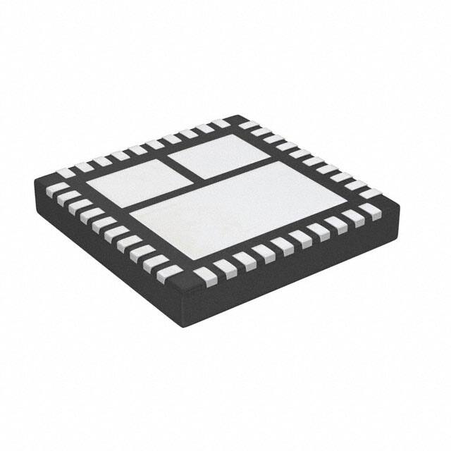
QFN40 6x6, 0.5P
CASE 485CM
PGND
•
•
•
•
•
•
•
•
•
•
•
•
•
(TOP VIEW)
ORDERING INFORMATION
Device
Package
Shipping†
NCP3232NMNTXG
QFN−40
(Pb−Free)
2500 /
Tape & Reel
†For information on tape and reel specifications,
including part orientation and tape sizes, please
refer to our Tape and Reel Packaging Specification
Brochure, BRD8011/D.
*For additional information on our Pb−Free strategy and soldering details, please
download the ON Semiconductor Soldering and Mounting Techniques
Reference Manual, SOLDERRM/D.
© Semiconductor Components Industries, LLC, 2015
May, 2021 − Rev. 9
1
Publication Order Number:
NCP3232N/D
�NCP3232N
VB
LDO
VCC
VCC
VB
VB
VB
BST
VIN
OSC
COMP
VREF
FB
VB
Control Logic
Ramp Generator
PWM Logic
+
E/A
−
− and −
SS
Soft Start
VCC
2 mA
EN
VB
VSWH
UVLO
OVP, UVP
Power Good
OCP, TSD
Protection
VSW
VB
Enable
Logic
1.2 V
POR
PGND
PG
VB
+
−
VREF
OTS
ISET
AGND
Figure 1. NCP3232N Block Diagram
www.onsemi.com
2
�NCP3232N
PIN DESCRIPTION
Pin No.
Symbol
1
SS
A capacitor from this pin to GND allows the user to adjust the soft−start ramp time.
Description
2
FB
Output voltage feedback.
3
COMP
4
ISET
5
AGND
6
OTS
7
PG
Power good indicator of the output voltage. Open−drain output. Connect PG to VDD with an external resistor.
8−14, EP42
VIN
The VIN pin is connected to the internal power NMOS switch. The VIN pin has high di/dt edges and
must be decoupled to ground close to the pin of the device.
15, 29−34,
EP43
VSWH
The VSWH pin is the connection of the drain and source of the internal NMOS switches. At switch
off, the inductor will drive this pin below ground as the body diode and the NMOS conducts with a
high dv/dt.
16−28, 37
PGND
Ground reference and high−current return path for the bottom gate driver and low- side NMOS
35
VSW
IC connection to the switch node between the top MOSFET and bottom MOSFET. Return path of
the high−side gate driver.
36
BST
Top gate driver input supply, a bootstrap capacitor connection between SWN and this pin.
38
VB
39
VCC
40
EN
EP41
GND
Output of the error amplifier.
A resistor from this pin to ground sets the over−current protection (OCP) threshold.
Analog ground.
Negative input of internal thermal comparator. Tie this pin to ground if not in use.
The internal LDO output and input supply for the charge pump. Connect a minimum of 4.7uF ceramic capacitor from this pin to ground.
Input Supply for IC. This pin must be connected to VIN.
Logic control for enabling the switcher. An internal pull−up enables the device automatically. The
EN pin can also be driven high to turn on the device, or low to turn off the device. A comparator
and precision reference allow the user to implement this pin as an adjustable UVLO circuit.
Exposed Pad. Connect GND to a large copper plane at ground potential to improve thermal dissipation.
www.onsemi.com
3
�NCP3232N
VIN
VIN
BST
VCC
VOUT
VSWH
VSW
VB
PGND
NCP3232N
ISET
AGND
VPG
EN
FB
OTS
PG
COMP
SS
1 MW
Figure 2. Typical Application Circuit
ABSOLUTE MAXIMUM RATINGS (measured vs. GND pad, unless otherwise noted)
Symbol
Rating
Power Supply to GND
Value
Unit
VIN, VCC
−0.3 to 23
V
VSW to GND
VSWH, VSW
−0.6 to 30 (DC)
−5(t
很抱歉,暂时无法提供与“NCP3232NMNTXG”相匹配的价格&库存,您可以联系我们找货
免费人工找货