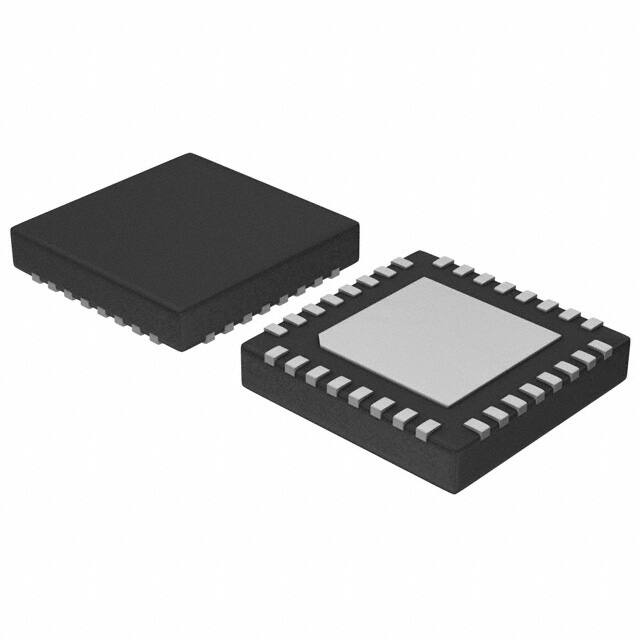
NCP81174N
4/3/2-Phase Synchronous
Buck Controller with Power
Saving Mode and PWM VID
Interface
www.onsemi.com
The NCP81174N is a general−purpose multi−phase synchronous
buck controller. It combines differential voltage sensing, differential
phase current sensing, and PWM VID interface to provide accurate
regulated power for the computer or graphic controllers. It can
receive power saving command (PSI) from processors and operates in
single−phase diode emulation mode to obtain high efficiency in light
load. Dual−edge current mode multiphase PWM modulation ensures a
fast transient response with minimum possible capacitors.
1
32
QFN32
MN SUFFIX
CASE 488AM
Features
•
•
•
•
•
•
•
•
•
•
•
•
•
•
MARKING DIAGRAM
Output Voltage up to 2.0 V with PWM VID Interface
Support 1.8 V VID Interface
Remote Differential Output Voltage Sense
Differential Current Sense for Each Phase
200 kHz − 1000 kHz Switching Frequency
PWMVID Frequency up to 5 MHz
Power Saving Interface (PSI)
Power Good Output
Thermally Compensated Current Monitoring
Over Current Protection
Fast Transient Response
Latched OVP and UVP Protections
QFN−32, 5 x 5 mm, 0.5 mm Pitch Package
This is a Pb−Free Device
1
81174N
AWLYYWWG
G
A
WL
YY
WW
G
(Note: Microdot may be in either location)
ORDERING INFORMATION
Typical Applications
• GPU and CPU Power
• Graphics Card Applications
© Semiconductor Components Industries, LLC, 2016
March, 2016 − Rev. 0
= Assembly Location
= Wafer Lot
= Year
= Work Week
= Pb−Free Package
Device
Package
Shipping†
NCP81174NMNTXG
QFN32
(Pb−Free)
2500 / Tape &
Reel
†For information on tape and reel specifications,
including part orientation and tape sizes, please
refer to our Tape and Reel Packaging Specifications
Brochure, BRD8011/D.
1
Publication Order Number:
NCP81174N/D
�G3
G2
G1
30
DRVON
31
G4
VREF
32
VCC
REFIN
NCP81174N
29
28
27
26
25
VIDBUF
1
24
CS4
VID
2
23
CS4N
VR_RDY
3
22
CS3
EN
4
21
CS3N
PSI
5
20
CS2
VINMON
6
19
CS2N
ROSC
7
18
CS1
ILIM
8
17
CS1N
NCP81174N
Top View
(not to scale)
13
14
15
16
VFB
VDFB
CSSUM
12
VDRP
11
COMP
10
DIFFOUT
VSP
9
VSN
FLAG/GND (Pin 33)
Figure 1. Pinout
www.onsemi.com
2
�NCP81174N
Figure 2. Typical Four Phase Application Circuit with PWM−VID Interface
www.onsemi.com
3
�NCP81174N
VID
UVP&OVP
VIDBUF
REFIN
G1
G2
PWM
Control
VSN
VSP
G3
G4
PSI
DIFFOUT
ILIM
EN
VFB
Fault Logic
UVLO
PGOOD
COMP
VR_RDY
VINMON
DRVON
VDFB
VDRP
CSSUM
VREF
CS1
CS1N
VREF
VCC
CS2
CS2N
CS3
Ramp
Generator
CS Amps
RSOC
CS3N
CS4
GND
CS4N
Figure 3. Functional Block Diagram
www.onsemi.com
4
�NCP81174N
PIN DESCRIPTION
Pin
Name
1
VIDBUF
Description
2
VID
3
VR_RDY
4
EN
Chip enable.
5
PSI
Power saving control. Three levels.
6
VINMON
7
ROSC
VID PWM pulse output from an internal buffer.
Voltage ID from processor.
Power good indicator.
Light input power rail monitor. It is a divided down voltage from the input power rail, should be kept to less
than 4 V at all time.
A resistance from this pin to ground programs the oscillator frequency.
8
ILIM
Over current shutdown threshold setting.
9
VSP
Non−inverting input to the internal differential remote sense amplifier.
10
VSN
Inverting input to the internal differential remote sense amplifier.
11
DIFFOUT
12
COMP
13
VFB
14
VDRP
Voltage signal proportional to the total current.
15
VDFB
Current summing amplifier inverting input
16
CSSUM
17
CS1N
18
CS1
19
CS2N
Output of the differential remote voltage sense amplifier.
Output of the compensation amplifier.
Inverting input of the compensation error amplifier
Current summing output signal
Inverting input to current sense amplifier, phase 1.
Non−inverting input to current sense amplifier, phase 1.
Inverting input to current sense amplifier, phase 2.
20
CS2
21
CS3N
Non−inverting input to current sense amplifier, phase 2.
22
CS3
23
CS4N
24
CS4
25
G1
Phase 1 PWM output, 3 levels.
26
G2
Phase 2 PWM output, 3 levels.
27
G3
Phase 3 PWM output, 3 levels.
28
G4
Phase 4 PWM output, 3 levels.
29
DRVON
30
VCC
5 V power supply for the chip.
31
VREF
2.0 V output reference voltage. A 10 nF ceramic capacitor is recommended to connect this pin to ground.
32
REFIN
Reference voltage input for output voltage regulation.
33
FLAG
Thermal pad and analog ground, connected to system ground.
Inverting input to current sense amplifier, phase 3.
Non−inverting input to current sense amplifier, phase 3.
Inverting input to current sense amplifier, phase 4.
Non−inverting input to current sense amplifier, phase 4.
Gate driver enable.
www.onsemi.com
5
�NCP81174N
MAXIMUM RATINGS
ELECTRICAL INFORMATION
Pin Symbol
VMAX
VMIN
ISOURCE
ISINK
COMP
5.5 V
−0.3 V
10 mA
10 mA
VDRP
5.5 V
−0.3 V
5 mA
5 mA
VSP
5.5 V
GND – 300 mV
1 mA
1 mA
VSN
GND + 300 mV
GND – 300 mV
1 mA
1 mA
DIFFOUT
5.5 V
−0.3 V
20 mA
20 mA
VR_RDY
5.5 V
−0.3 V
N/A
20 mA
VCC
7.0 V
−0.3 V
N/A
10 mA
ROSC
5.5 V
−0.3 V
1 mA
N/A
All Other Pins
5.5 V
−0.3 V
*All signals referenced to AGND unless otherwise noted.
THERMAL INFORMATION
Rating
Thermal Characteristic, QFN Package (Note 1)
Junction Temperature Range (Note 2)
Symbol
Value
Unit
RqJA
48.5
°C/W
TJ
−40 to 125
°C
Operating Ambient Temperature Range
TA
0 to 100
°C
Maximum Storage Temperature Range
TSTG
−55 to +150
°C
Moisture Sensitivity Level, QFN Package
MSL
1
Stresses exceeding those listed in the Maximum Ratings table may damage the device. If any of these limits are exceeded, device functionality
should not be assumed, damage may occur and reliability may be affected.
*The maximum package power dissipation must be observed.
1. JESD 51−5 (1S2P Direct−Attach Method) with 0 LFM.
2. JESD 51−7 (1S2P Direct−Attach Method) with 0 LFM.
www.onsemi.com
6
�NCP81174N
ELECTRICAL CHARACTERISTICS (VVCC = 5 V, VREFIN = 1.0 V, VPSI = 3.3 V, typical values are referenced to TA = 25°C, Min and
Max values are referenced to TA from 0°C to 100°C. unless other noted.)
Characteristics
Test Conditions
Symbol
Min
Typ
Max
Unit
1.5
2.5
mA
4.25
4.4
V
SUPPLY CURRENT
VCC Shutdown Current
EN < 0.95 V
ISHUT
VCC UVLO Rising
VCC UVLO Falling
4.0
4.10
V
SWITCHING FREQUENCY
Fsw
PS0 Switching Frequency Range
200
1000
kHz
10
%
2.0
2.05
V
1.98
2.0
2.02
V
Switching Frequency Accuracy
ROSC Output Voltage
VOLTAGE REFERENCE
VREF Reference Voltage
IREF = 1 mA
VVREF
PWM MODULATION
Minimum On Time (Note 3)
Fsw = 800 kHz
−
30
−
ns
0% Duty Cycle
COMP voltage when the PWM outputs
remain HI
−
1.3
−
V
100% Duty Cycle
COMP voltage when the PWM outputs
remain HI
−
2.3
−
V
PWM Phase Angle Error
Between adjacent phases
15
°
−15
VOLTAGE ERROR AMPLIFIER
Open−Loop DC Gain (Note 3)
100
dB
Unity Gain Bandwidth (Note 3)
10
MHz
Slew Rate (Note 3)
COMP Voltage Swing
5
3.5
−
−
V
ICOMP(sink) = 0.2 mA
−
−
50
mV
0
1.3
3
V
−50
0
50
nA
1.0
mV
200
nA
Non−inverting Voltage Range (Note 3)
Input Bias Current
Input Offset Voltage (Note 3)
V/ms
ICOMP(source) = 2 mA
VSP = VSN = 1.0 V
−1.0
CSx = CSxN = 1.0 V
−200
CURRENT−SENSE AMPLIFIER
Input Bias Current
0
Input Offset Voltage (Note 3)
−1.0
1.0
mV
Common Mode Input Range (Note 3)
−0.3
2.0
V
Differential Mode Input Range
−120
120
mV
6.3
V/V
Closed−Loop DC Gain (Note 3)
0 V < CSx − CSxN < 0.1 V
5.7
−3 dB Gain Bandwidth (Note 3)
6.0
10
Current Sharing Offset
−2.5
−
MHz
2.5
mV
CURRENT SUMMING AMPLIFIER
Current Sense Input to CSSUM DC Gain
−60 mV < CSx − CSxN < 60 mV
Current Sense Input to CSSUM −3 dB
Bandwidth (Note 3)
CL = 10 pF to GND, RL = 10 kW to
GND
CSSUM Output Slew Rate (Note 3)
−3.93
V/V
4
MHz
4
V/ms
Product parametric performance is indicated in the Electrical Characteristics for the listed test conditions, unless otherwise noted. Product
performance may not be indicated by the Electrical Characteristics if operated under different conditions.
3. Guaranteed by design, may not be tested.
www.onsemi.com
7
�NCP81174N
ELECTRICAL CHARACTERISTICS (VVCC = 5 V, VREFIN = 1.0 V, VPSI = 3.3 V, typical values are referenced to TA = 25°C, Min and
Max values are referenced to TA from 0°C to 100°C. unless other noted.)
Characteristics
Test Conditions
Symbol
Min
Typ
Max
Unit
CSSUM Summing Amp Output Offset
(Note 3)
−15
0
15
mV
Maximum CSSUM Output Voltage
3.0
CURRENT SUMMING AMPLIFIER
V
Minimum CSSUM Output Voltage
0.3
V
Output Source Current (Note 3)
1
−
−
mA
Output Sink Current (Note 3)
1
−
−
mA
−200
200
nA
−4.0
4.0
mV
DROOP AMPLIFIER VDRP
Input Bias Current (Note 3)
Input Offset Voltage (Note 3)
VSP = VSN = 1.1 V
Open Loop DC Gain (Note 3)
CL = 20 pF to GND including ESD
RL = 1 kW to GND
−
100
Open Loop Unity Gain Bandwidth
(Note 3)
CL = 20 pF to GND including ESD
RL = 1 kW to GND
−
10
−
MHz
Maximum Output Voltage
ISOURCE = 4.0 mA
3
−
−
V
Minimum Output Voltage
ISINK = 1.0 mA
−
−
1
V
Output source current (Note 3)
Vout = 3.0 V
4
−
−
mA
Output sink current (Note 3)
Vout = 1.0 V
1
−
−
mA
dB
REMOTE VOLTAGE DIFFERENTIAL SENSE AMPLIFIER
Input Bias Current (Note 3)
VSN = 0 V
30
mA
VSP Input Pull down Resistance
DRVON = low
DRVON = high
1.5
17
kW
VSP Input Bias Voltage (Note 3)
DRVON = low
DRVON = high
0.09
0.66
V
Input Voltage Range (Note 3)
−0.3
−
3.0
V
−
10
−
MHz
VSP −VSN = 0.5 to 1.3 V
0.98
1.0
1.025
V/V
3.0
−
−
V
−
−
0.5
V
3 dB Bandwidth (Note 3)
CL = 80 pF to GND,
RL = 10 kW to GND
Closed Loop DC gain
Maximum Output Voltage
ISOURCE = 2 mA
Minimum Output Voltage
ISINK = 2 mA
Output source current (Note 3)
Vout = 3 V
2.0
−
−
mA
Output sink current (Note 3)
Vout = 0.5 V
2.0
−
−
mA
Output High Voltage
Sourcing 500 mA
3.0
−
−
V
Output Low Voltage
Sinking 500 mA
−
−
0.7
V
Rise Time
CL (PCB) = 20 pF,
DVo = 10% to 90%
−
20
−
ns
Fall Time
CL (PCB) = 20 pF,
DVo = 10% to 90%
−
20
−
ns
EN rising
−
1.1
1.15
V
EN falling
0.95
1.0
DRVON
ENABLE
Enable Threshold
Product parametric performance is indicated in the Electrical Characteristics for the listed test conditions, unless otherwise noted. Product
performance may not be indicated by the Electrical Characteristics if operated under different conditions.
3. Guaranteed by design, may not be tested.
www.onsemi.com
8
�NCP81174N
ELECTRICAL CHARACTERISTICS (VVCC = 5 V, VREFIN = 1.0 V, VPSI = 3.3 V, typical values are referenced to TA = 25°C, Min and
Max values are referenced to TA from 0°C to 100°C. unless other noted.)
Characteristics
Test Conditions
Symbol
Min
Typ
Max
Unit
−
−
1.0
mA
ENABLE
EN Input Bias Current
External 1k pull−up to 3.3 V
POWER SAVE INPUT
PSI High Threshold (1.8 V input logic),
Refer to Table 1
Rising
Falling
1.4
1.2
1.55
V
1.05
PSI Low Threshold
Rising
Falling
0.8
0.6
0.95
V
0.5
−
−
1.0
mA
3.0
−
−
V
1.4
1.5
1.6
V
PSI Input Bias Current (Note 3)
PWM OUTPUTS
Output High Voltage
Sourcing 500 mA
Mid Output Voltage
Output Low Voltage
Sinking 500 mA
−
−
0.7
V
Rise Time
CL (PCB) = 50 pF,
DVo = 10% to 90%
−
10
15
ns
Fall Time
CL (PCB) = 50 pF,
DVo = 10% to 90%
−
10
15
ns
−
80
−
mA
210
240
265
mV
−
20
27
ms
4/3/2 PHASE DETECTION
Gate Pin Source Current
Gate Pin Threshold Voltage
Phase Detect Timer
VR_RDY – STARTUP
Vout Startup Delay
Measured from EN to Vout Start up
from 0 V
1.3
ms
VR_RDY Startup Delay
Measured from EN to VR_RDY
assertion, VBOOT = 0.9 V
1.9
ms
VR_RDY Shutdown Delay
Measured from EN to VR_RDY
de−assertion
200
350
ns
VR_RDY Low Voltage
IVR_RDY = 10 mA (sink)
−
−
0.4
V
VR_RDY Leakage Current
VR_RDY = 5 V
−
−
0.2
mA
0.95
1.0
1.05
V/V
PROTECTION – OCP, OVP, UVP
Current Limit ILIM to VDRP Gain
Current Limit ILIM to VDRP Gain in PSI
0.25
Current Limit ILIM Input Range
Under Voltage Protection (UVP)
Threshold
0
V/V
2.0
V
Relative to REFIN Voltage
50%
5
ms
Over Voltage Protection (OVP) Threshold Relative to REFIN Voltage
150%
REFIN
Over Voltage Protection (OVP) Threshold
Clamping Voltage
2
V
Over Voltage Protection (OVP) Delay
5
ms
Under Voltage Protection (UVP) Delay
REFIN
VINMON
0.94
VINMON Rising
1
V
Product parametric performance is indicated in the Electrical Characteristics for the listed test conditions, unless otherwise noted. Product
performance may not be indicated by the Electrical Characteristics if operated under different conditions.
3. Guaranteed by design, may not be tested.
www.onsemi.com
9
�NCP81174N
ELECTRICAL CHARACTERISTICS (VVCC = 5 V, VREFIN = 1.0 V, VPSI = 3.3 V, typical values are referenced to TA = 25°C, Min and
Max values are referenced to TA from 0°C to 100°C. unless other noted.)
Characteristics
Test Conditions
Symbol
Min
Typ
Max
Unit
0.65
0.87
V
VINMON
VINMON Falling
PWM−VID BUFFER
Buffer Output Rise Time
Tr
3
ns
Buffer Output Fall Time
Tf
3
ns
Rising and Falling Edge Delay (Note 3)
DT = |Tr − Tf|
DT
Propagation Delay
Tpd = TpHL = TpLH
Tpd
Propagation Delay Error (Note 3)
DTpd = TpHL – TpLH
0.5
8
DTpd
ns
ns
0.5
ns
REFIN
REFIN Discharge Switch ON−Resistance
IREFIN (sink) = 2 mA
REFIN Discharge Time (Note 3)
Measured from EN assertion
6
W
100
ms
Product parametric performance is indicated in the Electrical Characteristics for the listed test conditions, unless otherwise noted. Product
performance may not be indicated by the Electrical Characteristics if operated under different conditions.
3. Guaranteed by design, may not be tested.
www.onsemi.com
10
�NCP81174N
DETAILED DESCRIPTION
General
inductor and capacitors. Introduction of dual−edge current
mode multi−phase control results in fast transient response
and good dynamic current balance.
The NCP81174N, a 4/3/2−phase synchronous buck
controller with PWM VID interface in a QFN−32 package,
provides a compact−footprint power management solution
for new generation computing and graphic processors. It
receives power saving input (PSI) from processors and
operates in 1−phase forced PWM or diode emulation mode
to obtain high efficiency in light−load conditions. It can
either receive PWMVID from the processor to achieve
dynamic voltage control or locally set the reference from an
internal precise 2 V regulator. Operating in high switching
frequency up to 1 MHz allows employing small size
Power Operation Modes
The NCP81174N has 3 power operation modes
corresponding to PSI levels as shown in Table 1. The chip
is compatible to different I/O systems. The configuration
would follow Table 1, the ENABLE signal needs to be
higher than 1.1 V only to turn on the chip. The operation
mode can be changed on the fly.
Table 1. POWER SAVING INTERFACE (PSI) CONFIGURATIONS (1.8 V I/O, 2.5 V > EN > 1.1 V)
PSI Level
Power Mode
Phase Configuration
High (PSI ≥ 1.4 V)
PS0
Full Phase, FCCM
Intermediate (0.8 V < PSI < 1.4 V)
PS1
1−Phase, FCCM
Low (PSI ≤ 0.8 V)
PS2
1−Phase, Auto CCM/DCM
Remote Voltage Sense
Switching Frequency
A true differential amplifier allows the NCP81174N to
measure Vcore voltage feedback with respect to the Vcore
ground reference point by connecting the Vcore reference
point to VSP, and the Vcore ground reference point to VSN.
This configuration keeps ground potential differences
between the local controller ground and the Vcore ground
reference point from affecting regulation of Vcore between
Vcore and Vcore ground reference points. The remote
sensing amplifier also subtracts the REFIN (DAC) voltage,
thereby producing an unamplified output error voltage at the
DIFFOUT pin. This output also has a 1.3 V bias voltage as
the floating ground to allow both positive and negative error
voltages.
The Rosc pin provides a 2.0 V reference voltage. The
resistor connected to this pin will sink current from the pin
to ground. This current is internally mirrored into a capacitor
to create an oscillator. The period is proportional to the
resistance and the frequency is inversely proportional to the
total resistance. The total resistance may be estimated by
Equation 1. This equation is valid for the individual phase
frequency in multi−phase mode PS0 and single phase mode
PS1. In PS2, the frequency will be close to set frequency in
CCM and scaled down with load current in DCM operation.
Rosc ^ 20947 @ F SW −1.1262
(eq. 1)
ROSC vs. FREQ
60
Calculation
REFIN
Real
50
Rosc−kohm
40
VSN
30
VSP
20
10
0
100
DIFFOUT
1000
Freq−kHz
Figure 5. ROSC vs. Frequency
Figure 4. Voltage Remote Sense
www.onsemi.com
11
�NCP81174N
PWM VID
V max + Vref @
The NCP81174N receives the PWMVID signal from the
upstream controller for the Vcore regulation. The signal is
decoded internally and passed to the VID buffer output
(VIDBUF), where the duty cycle is converted to a
corresponding signal between 0 V and 2 V. The VIDBUF
high level is derived from a precise 2.0 V reference voltage.
The VIDBUF signal is then filtered through the external low
pass filter constructed by R_REFADJ and C_REFIN. The
filtered output is connected to the REFIN pin. The REFIN
is the voltage reference of the Vcore regulator. The output
voltage maximum, minimum, and also boot voltage can be
calculated with below equations.
V min + Vref @
R_VREF2
(eq. 2)
R VREF2 ) ǒR_VREF1 ø R_REFADJǓ
R_VREF1 ø R_REFADJ
(eq. 3)
R_VREF1 ) ǒR_VREF1 ø R_REFADJǓ
V boot +
V max ) V min
(eq. 4)
2
VREF
R _VREF1
VIDBUF
REFIN
R _REFADJ
PWMVID
C_ REFIN
R _VREF2
Figure 6. PWM VID Interface
PWM Comparators with Hysteresis and 3rd State of
PWM Outputs
Soft Start
The NCP81174N has an internal controlled soft start
function. The output starts to ramp up following a system
reset period after the device is enabled. The device is able to
start up smoothly under an output pre−biased condition
without discharging the output before ramping up.
Before the output soft start begins, an internal switch will
be turned on to discharge the external filter capacitor
C_REFIN connected to the REFIN pin to reset the DAC
setting, the typical on resistance of the switch is around 6 Ws.
After the discharging, internal switch will be turned off to
allow external C_REFIN capacitor to recharge. After ~
100 ms interval, the output voltage ramps up with a fixed
slew rate.
The circuit can be set to start from either all the phases
when the input power rails are all available or from phase 1
when only one input power rail is available by presetting the
power mode from PSI pin (See Power Operation Modes).
Four PWM comparators receive an error signal at their
non−inverting input and one of the triangle waves at its
inverting input. The output of each comparator generates the
PWM outputs G1, G2, G3 and G4.
During the steady state operation, the duty cycle will
center on the valley of the triangle waveform, with steady
state duty cycle calculated by Vout/Vin. During a transient
event, both high and low comparator output transitions shift
phase to the points where the error signal intersects the down
and up ramp of the triangle wave.
PWM signals vary between high and low in all phase
operation or forced PWM mode. In power saving mode
(PS2), PWM signals vary between high and mid level to
allow diode emulation.
2/3/4 Phase Operation
Besides 4−phase, the part can be configured to run in 2 or
3−phase mode. In 2−phase mode, phase 1 and 3 should be
used to drive the external gate drivers, gate outputs G2 and
G4 should be grounded. In 3−phase mode, gate output G4
should be grounded. The current sense inputs of the unused
channels should be connected to the Vcore output.
Thermal Compensation Amplifier with VDRP and
VDFB Pins
Thermal compensation amplifier is an internal amplifier
in the path of droop current feedback for additional
adjustment of the gain of summing current and temperature
compensation. The way thermal compensation is
implemented separately ensures minimum interference to
the voltage loop compensation network.
www.onsemi.com
12
�NCP81174N
Differential Current Sense Amplifiers and Summing
Amplifier
Over Current Protection and Under Voltage Protection
A programmable overcurrent function is incorporated
within the IC. The inverting input of the comparator is
connected to the ILIM pin. The voltage at this pin (0~2 V)
sets the maximum output current the converter can produce.
The VREF pin provides a convenient and accurate reference
voltage from which a resistor divider can create the
overcurrent setpoint voltage. Although not actually
disabled, tying the ILIM pin directly to the VREF pin sets the
limit above useful levels − effectively disabling overcurrent
shutdown. The comparator non−inverting input is the
summed current information from the current sense
amplifier. The overcurrent event will set PWM low for the
rest of the cycle when the current information exceeds the
voltage at the ILIM pin. If the overcurrent continuously
happens and the output will eventually hit the Under Voltage
Protection (UVP) limit and it will be a latched event. The
UVP limit is set to 50% below the REFIN voltage. The
PWM outputs will stay at mid state until the VCC voltage is
removed and re−applied, or the ENABLE input is brought
low and then high.
Four differential amplifiers are provided to sense the
output current of each phase. The inputs of each current
sense amplifier must be connected across the current sensing
element of the phase controlled by the corresponding gate
output (G1, G2, G3, or G4). If a phase is unused, the
differential inputs to that phase’s current sense amplifier
must be shorted together and connected to the output.
A voltage is generated across the current sense element
(such as an inductor or sense resistor) by the current flowing
in that phase. The outputs of four current amplifiers are fed
into a summing amplifier to have a summed−up output
(CSSUM). Signal of CSSUM combines information of total
current of all phases in operation. The gain from the total
sense current input to CSSUM (ACSSUM) is ~3.93.
The output of the current sense amplifiers are used to
control three functions. First, the output controls the
adaptive voltage positioning, where the output voltage is
actively controlled according to the output current. Second,
the output signal is fed to the current limit circuit. This again
is the summed current of all phases in operation. Finally, the
individual phase current is connected to the PWM
comparator. In this way current balance is accomplished.
Over Voltage Protection
An output voltage monitor is incorporated. During normal
operation, if the output voltage is 50% over the REFIN, the
VR_RDY goes low, the DRVON signal remains high, and
PWM outputs are set low. The limit will be clamped to 2 V
if 50% over REFIN creates a voltage above the 2 V. The
outputs will remain disabled until the VCC voltage is
removed and reapplied, or the ENABLE input is brought
low and then high.
Undervoltage Lockout (VCC UVLO) and VINMON
VCC is constantly monitored for undervoltage lockout
(UVLO). Line input (VIN) is monitored for undervoltage
lockout through VINMON pin by connecting an appropriate
resistor divider from line input to the VINMON input. The
setting of the resistor divider should make the VINMON
voltage less than 4 V at all time. During power-up both VCC
and VINMON will be monitored. Only after they exceed
their individual UVLO thresholds, the full circuit will be
activated and ready for soft start if the enable pin is also
valid. Both UVLO comparators have hysteresis to avoid
chattering. The second function of VINMON pin is to
provide feed-forward input voltage information in PS2
mode, see Power Operation Mode section.
www.onsemi.com
13
�NCP81174N
DESIGN METHODOLOGY
Programming the Current Limit
Acssum
RNOR
The VREF pin provides a 2.0 V reference voltage which
is divided down with a resistor divider (RLIM1/RLIM2) and
fed into the current limit pin ILIM. The current limit
function is based on the total sensed current of all phases
multiplied by a controlled gain (Acssum*Adrp). DCR
sensed inductor current is a function of the winding
temperature. If not using thermal compensation, the best
approach is to set the maximum current limit based on
expected average maximum temperature of the inductor
windings,
I1
RISO1
RSUM
+
Ilim
Figure 7. ACSSUM and ADRP
As introduced before, VLIMIT comes from a resistor
divider connected to VREF, thus
V LIMIT + 2 V @
(eq. 6)
@
ǒ
I MIN_OCP @ ) 0.5 @
A DRP + −
(eq. 7)
R LIM1 ) R LIM2
@ COEpsi
(eq. 8)
R NOR @ ǒR ISO1 ) R ISO2 ) R T2Ǔ (eq. 9)
ǒR NOR ) R ISO1 ) R ISO2 ) R T2Ǔ @ R SUM
RISO1 and RISO2 are in series with RT2, the NTC
temperature sense resistor placed near inductor. RSUM is
the resistor connecting between pin VDFB and pin CSSUM.
In PS0 mode, the current limit follows the Equation 10; In
PS1 or PS2, the current limit calculation follows
Equation 11, COEpsi is a coefficient for the current limiting
related in power saving mode PS1, PS2. COEpsi value is one
over the original phase count N. Refer to the PSI and phase
shedding section for more details.
Ǔ
ǒV in * N @ V outǓ @ V out
L @ F SW @ V in
R LIM2
A CSSUM X+ −3.93
V LIMIT ^ A CSSUM @ A DRP @ DCR TMAX
V LIMIT ^ A CSSUM @ A DRP @ DCR TMAX
OCP
event
−
Therefore calculate the current limit voltage as below,
@ ǒI MIN_OCP @ ) 0.5 @ I PPǓ
+
I4
For multiphase controller, the ripple current can be
calculated as,
L @ F SW @ V in
−
+
I3
(eq. 5)
ǒV in * N @ V outǓ @ V out
RT2 RISO2
I2
DCR Tmax + DCR 25o @ (1 ) 0.00393 @ (T max * 25))
I PP +
Adrp
In Equation 7, ACSSUM and ADRP are the gain of current
summing amplifier and droop amplifier.
2 V@R LIM2
RLIM1)RLIM2
I LIMIT(normal) ^
3.93 @
RNOR@ǒR ISO1)RISO2)RT2Ǔ
ǒRNOR)RISO1)RISO2)RT2Ǔ@RSUM
ǒV in * N @ V outǓ @ V out
* 0.5 @
2 V@R LIM2
L @ F SW @ V in
I LIMIT(PSI) ^
3.93 @
@ DCR 25° @ ǒ1 ) 0.00393 @ ǒT inductor * 25ǓǓ
RLIM1)RLIM2
RNOR@ǒRISO1)RISO2)RT2Ǔ
ǒRNOR)RISO1)RISO2)RT2Ǔ@RSUM
ǒV in * V outǓ @ V out
* 0.5 @
(eq. 10)
@ COEpsi
@ DCR 25° @ ǒ1 ) 0.00393 @ ǒT inductor * 25ǓǓ
(eq. 11)
L @ F SW @ V in
The first cut approach is to use a 0.1 mF capacitor for C and
then solve for R.
N is the number of phases involved in the circuit.
Inductor Current Sensing Compensation
The NCP81174N uses the inductor current sensing
method. An RC filter is selected to cancel out the impedance
from inductor and recover the current information through
the inductor’s DCR. This is done by matching the RC time
constant of the sensing filter to the L/DCR time constant.
R sense(T) +
L
(eq. 12)
0.1 @ mF @ DCR 25C @ (1 ) 0.00393 @ (T * 25))
Because the inductor value is a function of load and
inductor temperature final selection of R is best done
experimentally on the bench by monitoring the VDRP pin
and performing a step load test on the actual solution.
www.onsemi.com
14
�NCP81174N
Compensation and Output Filter Design
E1
+
R14
−
V3
Voff
E
C6
0
0
0 12
1
L
2
DCR
1
LBRD
RBRD
2
0
VRamp_min
CBulk
CCer
RSUM
ESRBulk
ESRCer
2
2
RDFB
ESLBulk
Vout
ESLCer
R8
Voff
1E4
1
1
Vdrp
C5
0
C_REFIN
R_VIDBUF
R12
COMP
PWMVID
0
R_VREF2
CFB1
CH
RFB1
CF
VREF
2.0V
0
REFIN
0
RF
R_VREF1
0
RFB
V4
R6
Voff
1E4
Voffset
C4
0
0
Figure 8. System Average Model
CH
A simple state average model shown in Figure 8 can be
used to assist the system design and determine a stable
solution.
The goal is to compensate the system such that the
resulting gain generates constant output impedance from
DC up to the frequency where the ceramic takes over
holding the impedance below the target output impedance.
By matching the following equations a good set of starting
compensation values can be found for a typical mixed bulk
and ceramic capacitor type output filter.
RFB1
1
+
1
RF
CF
RFB
I Bias
−
+
+
1.3 V
RDRP
Droop
Amp
RT
RISO2
−
Error
Amp
PWM
Comparator
+
−
RNOR
1.3 V
RISO1
RSUM
Gain = 4
−
(eq. 13)
1
1
+
2p @ CF @ RF
2p @ (RBRD ) ESRBulk) @ CBulk
2p @ CFB1 @ (RFB1 ) RFB)
CFB1
+
CSSUM
Amp 1.3 V
RSx
(eq. 14)
+
+
RL
+
−
2p @ CCer @ (RBRD ) ESRBulk)
Gain = 1
CSx
Droop Injection and Thermal Compensation
Figure 9. Droop Injection and Thermal Compensation
The VDRP signal is generated by summing the sensed
output currents for each phase. A droop amplifier is added
to adjust the total gain to approximately eight. VDRP is
externally summed into the feedback network by the resistor
RDRP. This introduces an offset which is proportional to the
output current thereby forcing a controlled, resistive output
impedance.
RDRP determines the target output impedance by the
basic equation:
V out
I out
+ Z out +
R FB @ DCR @ A CCSUM @ A DRP
R DRP +
www.onsemi.com
15
R DRP
R FB @ DCR @ A CSSUM @ A DRP
Z out
(eq. 15)
(eq. 16)
�NCP81174N
nonlinear. Putting a resistor in series with the NTC helps
make the device appear more linear with temperature. The
series resistor is split and inserted on both sides of the NTC
to reduce noise injection into the feedback loop. The
recommended total value for RISO1 plus RISO2 is
approximately 1.0 kW.
The output impedance varies with inductor temperature
by the equation:
The value of the inductor’s DCR is a function of
temperature according to Equation 17:
DCR(T) + DCR 25C @ (1 ) 0.00393 @ (T * 25))
(eq. 17)
Actual DCR increases by temperature. The system can be
thermally compensated to cancel this effect to a great degree
by adding an NTC in parallel with RNOR to reduce the
droop gain as the temperature increases. The NTC device is
Z out(T) +
R FB @ DCR 25C @ (1 ) 0.00393 @ (T * 25)) @ A CSSUM @ A DRP
(eq. 18)
R DRP
By including the NTC RT2 and the series isolation
resistors the new equation becomes:
R FB @ DCR 25C @ (1 ) 0.00393 @ (T * 25)) @ A CSSUM @
Z out(T) +
RNOR@ǒRISO1)RISO2)RT2Ǔ
ǒRNOR)RISO1)RISO2)RT2Ǔ@RSUM
(eq. 19)
R DRP
The typical equation of an NTC is based on a curve fit Equation 20:
RT2(T) + RT2 25C @ e b
ƪǒ2731) TǓ * ǒ2981 Ǔƫ (eq. 20)
Zout vs Temperature
0.0013
Zout
Figure 10 shows an example of the comparison of the
compensated output impedance and uncompensated output
impedance varying with temperature.
0.0012
Zout(uncomp)
Ohm
0.0011
0.001
0.0009
0.0008
0.0007
0.0006
25
45
65
85
105
Celsius
Figure 10. Zout vs. Temperature (10 kW NTC with a b
value of 3740)
www.onsemi.com
16
�NCP81174N
SYSTEM TIMING DIAGRAM
VIN
5V, VCC
EN
1.8V
1.1mS
PWMVID, 1V
DRVON


 工商网监
湘ICP备2023018690号
工商网监
湘ICP备2023018690号
