Synchronous Buck
Controller with 2-Bit VID
Inputs
NCP5269B
•
•
•
•
•
•
•
•
•
•
•
•
•
•
•
•
•
Wide Input Voltage Range: from 3.3 V to 28 V
Three Selectable Fixed Frequency 300 kHz, 400 kHz or 600 kHz
2−Bit VID Selects Four Independent Voltages from 0.65 V to 1.5 V
±1.0% System Accuracy
Differential Remote Output Voltage Sensing
Soft Transient Control Reduces Inrush Current and Audio Noise
Build−in Power−Good Masking Supports Voltage Identification
(VID) On−The−Fly Transients
Simple Resistor Programming Voltage Levels
Programmable Soft−Start through a Single Capacitor
Forced CCM Operation
Input Supply Voltage Feed Forward Control
Resistive or Lossless Inductor’s DCR Current Sensing
Over−Temperature Protection
Built−in Adaptive Gate Drivers
Output Discharge Operation
Built−in Over−Voltage, Under−Voltage and Over−Current Protection
and Power Good Output
This is a Pb−Free Device
Applications
•
•
•
•
•
Notebooks, Desktops & Servers
DDR Termination Voltage
I/O Supplies
System Power Supplies
Graphic Cards
© Semiconductor Components Industries, LLC, 2013
September, 2020 − Rev. 0
MARKING
DIAGRAM
5269B
ALYWG
G
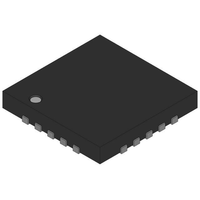
20 PIN QFN, 3x3
MN SUFFIX
CASE 485BC
5269B
A
L
Y
W
G
= Specific Device Code
= Assembly Location
= Wafer Lot
= Year
= Work Week
= Pb−Free Package
(Note: Microdot may be in either location)
PIN CONNECTIONS
COMP
FB
FBRTN
CSN
CSP
Features
www.onsemi.com
EN
VCC
VID1
VID0
V3
1
AGND
BST
GH
SWN
VCCP
GL/FSET
V2
V1
VREF
PG
PGND
NCP5269B is a synchronous buck controller that is optimized for
converting the battery voltage or adaptor voltage into power supply
rails required in notebook and desktop system. NCP5269B is designed
for applications requiring dynamically selected slew−rate controlled
output voltages. The soft−start is programmed by a single capacitor.
Voltage identification logic−inputs select four resistor programmed
set−point reference voltages that directly set the output voltage of the
converter between 0.65 V to 1.5 V. NCP5269B supports high
efficiency, fast transient response and provides power good signal.
Forced CCM operation provides DDR termination voltage with
source/sink capability. The part operates with input voltage ranging
from 3.3 V to 28 V. NCP5269B is available in a 20−pin 3 mm x 3 mm
QFN package.
(Top View)
ORDERING INFORMATION
Device
Package
Shipping†
NCP5269BMNTWG
QFN20
(Pb−Free)
3000 /
Tape & Reel
†For information on tape and reel specifications,
including part orientation and tape sizes, please
refer to our Tape and Reel Packaging Specification
Brochure, BRD8011/D.
1
Publication Order Number:
NCP5269B/D
�NCP5269B
VID0
VID1
Precision
Reference
VID
Decoder &
Vref
Selection
V3
V2
V1
VREF
+
−
Internal
Reference
FBRTN
FB
+
E/A
−
OC & TRE Detection
BST
COMP
Control Logic
Ramp Generator
And
PWM Logic
CSP
CSN
CSA
GH
SW
+
−
VCC
VCCP
UVLO,
UVP, OVP,
Power Good
OCP, TSD and
Protection
EN
PG
AGND
Figure 1. Block Diagram
www.onsemi.com
2
GL/FSET
PGND
�NCP5269B
Table 1. PIN DESCRIPTIONS
Pin
No.
Symbol
1
EN
2
VCC
Supply for analog circuit.
3
VID1
Logic input for reference voltage selector. Use in conjunction with the VID0 pin to select among four set−point
reference voltages.
4
VID0
Logic input for reference voltage selector. Use in conjunction with the VID1 pin to select among four set−point
reference voltages.
5
V3
Voltage set−point programming resistor input.
6
V2
Voltage set−point programming resistor input.
7
V1
Voltage set−point programming resistor input. External reference input when enabled by connecting the V3 pin
to the VCC pin.
8
VREF
9
PG
10
PGND
11
GL/FSET
12
VCCP
Power supply for MOSFET gate drive
13
SWN
Switch node between the top MOSFET and bottom MOSFET.
14
GH
Gate driver output of the top N−channel MOSFET.
15
BST
Top gate driver input supply, a bootstrap capacitor connection between SWN and this pin.
16
CSP
Inductor current differential sense non−inverting input.
17
CSN
Inductor current differential sense inverting input.
18
FBRTN
Description
Logic control for enabling the switcher. Applying greater than 1.4 V will turn on the part. Connect to GND to
disable.
Soft−start programming capacitor input. Set-point reference voltage programming resistor input. Connects
internally to the inverting input of the VSET voltage set-point amplifier.
Power good indicator of the output voltage. Open−drain output.
Ground reference and high−current return path for the bottom gate driver.
Gate driver output of bottom N−channel MOSFET. And it is also used to set up switching frequency by
connecting a resistor from this pin to ground.
Feedback Return Input/Output. This pin remotely senses the output voltage. It is also used as the ground
return for the VID reference voltage and the voltage error amplifier blocks.
19
FB
20
COMP
Output voltage feed back.
Output of the error amplifier.
AGND
Analog ground. Bottom thermal pad.
www.onsemi.com
3
�NCP5269B
C2
R3
C3 R1
R2
FB
CSN CSP
20
1
VCC
5.0 V
2
VID1
3
VID0
4
V3
VIN
R4
COMP
EN
FBRTN
C1
19
17
BST
15
AGND
V2
9
V1
Cout
CVCCP
10
PG
Lo
GL/FSET
11
8
V CCP
5 .0 V
VCCP
12
7
Vout
SWN
13
VREF
CBOOT
GH
14
6
Cin
16
FBRTN
5
Rset4
18
PGND
CSS
VCC
PG
Rset3
Rset2
Rset1
FBRTN
Figure 2. Application Circuit
Table 2. ABSOLUTE MAXIMUM RATINGS
Rating
Value
VCC to AGND
−0.3 V (DC) to 6.5 V
FBRTN, PGND
−0.3 V to +0.3 V
SWN to PGND
−5.0 V to 28 V, −10.0 V for T < 100 ns
BST, GH to GND
−0.3 V to 34 V
BST to SWN, GH to SWN, VCC to PGND, DL to PGND
−0.3 V to 6.5 V
All other pins
−0.3 V to 6.5 V
Operating Temperature Range, TA
−40°C to +100°C
Junction Temperature, TJ
−40°C to +100°C
Storage Temperature Range, TS
−55°C to +150°C
Package Characteristic
Thermal Resistance from Junction−to−Ambient (TA = +25°C), Rthja
35 °C/W (Note 1)
Stresses exceeding those listed in the Maximum Ratings table may damage the device. If any of these limits are exceeded, device functionality
should not be assumed, damage may occur and reliability may be affected.
1. This data is for solder on 4−layer board with 2 oz. copper.
www.onsemi.com
4
�NCP5269B
Table 3. ELECTRICAL CHARACTERISTICS
(VCC = VCCP = 5.0 V, Vout = 1.0 V, TA = +25°C for typical value; −40°C < TA < 100°C for min/max values unless noted otherwise)
Parameter
Symbol
Test Conditions
Min
Typ
Max
Units
POWER SUPPLY
VCC Operation Voltage
VCC
4.5
5
5.5
V
VCCP Operation Voltage
VCCP
4.5
5
5.5
V
3.9
4.2
4.45
V
300
350
400
mV
230
300
mV
1.0
mA
VOLTAGE MONITORING & PROTECTION
VCC Start Threshold
VCC UVLO Hysteresis
Power Good Low Voltage
IPG(sink) = 4 mA
Power Good High Leakage Current
Power Good Startup Delay (Note 2)
Power Good Propagation Delay
Power Good Threshold
Measure from SSEND to PG
pos edge
3.3
ms
Delay for power good in
3.3
ms
Delay for power good out
1.5
ms
Power Good in from high
101.5
105
107.5
%
Power Good in from low
92.5
95
98.5
%
PG hysteresis
Power Good Masking Time
FB Overvoltage Threshold
5
Triggered by any VID Change
VOVFB−VID
Relative to nominal VID Voltage
%
425
150
200
ms
250
mV
Overvoltage Propagation Delay
1.5
ms
FB Over Voltage Threshold During Soft−
Start
2.0
V
FB Under−Voltage Trip Threshold
VUVFB−VID
Relative to nominal VID Voltage
−360
Undervoltage Protection Blanking Time
−300
−240
3.3
mV
ms
SUPPLY CURRENT
VCC Quiescent Current
VCC Shutdown Supply Current
VCCP Quiescent Current
VCCP Shutdown Supply Current
BST Quiescent Current
BST Shutdown Supply Current
IVCC
Vskip = 0 V, VFB = 1.5 V, EN = 5.0
(No Switching),
GH and GL are open
IVCC_SD
3.9
5
mA
EN = 0 V
3
mA
IVCCP
Vskip = 0 V, VFB = 1.5 V, EN = 5.0
(No Switching),
GH and GL are open
0.3
mA
IVCCP_SD
EN = 0 V
1
mA
IBST
Vskip = 0 V, VFB = 1.5 V, EN = 5.0
(No Switching),
GH and GL are open
0.33
mA
IBST_SD
EN = 0, BST = 5 V, SWN = 0
1
mA
FEEDBACK VOLTAGE
Reference Voltage
VREF
V
0.65
System Accuracy
VID0 = VID1 = High,
PWM in CCM mode,
−40°C < TA < 100°C
−1.0
+1.0
TA = 25°C
−0.35
+0.35
%
Feedback Voltage Line Regulation
Vcc = 4.5 V ~ 5.5 V
0.75
%/V
2. Guaranteed by characterization or correlation, not production tested
www.onsemi.com
5
%
�NCP5269B
Table 3. ELECTRICAL CHARACTERISTICS
(VCC = VCCP = 5.0 V, Vout = 1.0 V, TA = +25°C for typical value; −40°C < TA < 100°C for min/max values unless noted otherwise)
Parameter
Symbol
Test Conditions
Min
Typ
Max
Units
VOLTAGE ERROR AMPLIFIER
80
Open Loop DC Gain (Note 2)
Open Loop Unity Gain Bandwidth
(Note 2)
F0dB,EA
dB
20
FB Input Voltage Range (Note 2)
0
FB Bias Current (Note 2)
Relative to CSN = VID
Slew Rate
Maximum Output Voltage
10 mV of overdrive,
ISOURCE = 2.0 mA
Minimum Output Voltage
10 mV of overdrive,
ISINK = 2.0 mA
2.0
1
−1
COMP pin to GND = 10 pF
3.3
MHz
V
mA
10
V/ms
3.5
V
0.2
0.3
V
Output Source Current
10 mV of overdrive, Vout = 3.5 V
2
mA
Output Sink Current
10 mV of overdrive, Vout = 1.0 V
2
mA
Refer to AGND
−0.2
2.0
V
−30
30
mV
DIFFERENTIAL CURRENT SENSE AMPLIFIER
CSP and CSN Common−mode Input
Voltage Range
Differential Input Voltage Range
OVER CURRENT PROTECTION
V(CSP)−V(CSN),
Vo = 1 V
Vo = 0.5 V ~ 1.5 V
OCP Threshold
27
26
30
30
33
34
mV
2_BITS VID
0.65
VID0, VID1 High Threshold Voltage
V
VID0, VID1 Low Threshold Voltage
0.4
VID0, VID1 Input Bias Current
VID = 0 V
V
1
nA
VID0, VID1 Pull Down Current
2.5
mA
Charging current during VID up (Note 2)
73
mA
Discharging current during VID down
(Note 2)
90
mA
VID Delay time
Any VID edge to 10% of FB
change
200
ns
1.4
V
EN
EN High Threshold Voltage
EN Low Threshold Voltage
EN Input Bias Current
IEN
EN = 5 V
EN Input Voltage
0.4
V
10
mA
5.5
V
PWM
30
Minimum Controllable ON Time (Note 2)
Minimum OFF Time (Note 2)
300
PWM Ramp Amplitude (Note 2)
500
ns
VIN = 5 V
1.25
V
VIN = 12 V
3
V
2. Guaranteed by characterization or correlation, not production tested
www.onsemi.com
6
400
ns
�NCP5269B
Table 3. ELECTRICAL CHARACTERISTICS
(VCC = VCCP = 5.0 V, Vout = 1.0 V, TA = +25°C for typical value; −40°C < TA < 100°C for min/max values unless noted otherwise)
Parameter
Symbol
Test Conditions
Min
Typ
Max
Units
INTERNAL BST DIODE
Forward Voltage Drop
Reverse−bias Leakage Current
IF = 10 mA, TA = 25°C
0.3
V
VBST = 34 V, VSW = 28 V,
TA = 25°C
0.1
1
mA
EN = 0, Vout = 0.65 V
14
30
W
SOFT STOP
Output Discharge On−Resistance
Discharge Threshold in Vcc
0.6
V
20
mA
SOFT START
Soft Start Current
ISS
OSCILLATOR
Oscillator Frequency
FSW
Rset = 2K
270
300
Oscillator Frequency Accuracy
330
KHz
±10
%
GATE DRIVER
GH Pull−High Resistance (Note 2)
RH_GH
Source, V(BST−GH) = 0.1
1.3
1.8
W
GH Pull−Low Resistance (Note 2)
RL_GH
Sink, V(GH−SWN) = 0.1 V
1.1
1.6
W
GL Pull−High Resistance (Note 2)
RH_GL
Source, V(VCC−GL) = 0.1 V
1.0
1.8
W
GL Pull−Low Resistance (Note 2)
RL_GL
Sink, V(GL−PGND) = 0.1 V
0.5
0.9
W
GH Source Current
2
A
GH Sink Current
2
A
GL Source Current
2
A
GL Sink Current
4
A
Dead Time
GL off to GH on
10
20
30
GH off to GL on
10
20
30
ns
THERMAL SHUTDOWN
Thermal Shutdown Threshold (Note 2)
150
°C
Thermal Shutdown Hysteresis (Note 2)
25
°C
2. Guaranteed by characterization or correlation, not production tested
www.onsemi.com
7
�NCP5269B
DETAILED DESCRIPTION
VOUT
R1
FB
−
Overview
E/A
COMP
+
NCP5269B is designed for applications requiring
dynamically selected slew−rate controlled output voltages.
It provides a synchronous PWM controller that incorporates
all the control and protection circuitry necessary to satisfy a
wide range of applications. Forced CCM operation provides
DDR termination voltage with source/sink capability It also
provides fast transient response and excellent stability. The
features of the NCP5269B include a 2 bits VID selectable
and external programmable reference, fixed three preset
switching frequency, an error amplifier, adaptive gate
driver, programmable soft−start, and very low shutdown
current. The protection features of the NCP5269B include
over−current protection, power good monitor, over voltage
and under voltage protection, built in output discharge and
thermal shutdown.
R2
Vset
VREF
SW0
V1
SW1
V2
SW2
V3
SW3
R3
CSS
R4
FBRTN
R5
Reference Voltage Programming
R6
The NCP5269B incorporates 2−bits VID, which selects
four user−programmed reference voltages that reflect on
Vref pin. NCP5269B measures VFB and VREF pin voltage
relative to FBRTN pin. An internal reference that allows
output voltages as low as 0.65 V. The tolerance of the
internal reference is guaranteed over the entire operating
temperature range of the controller. The reference voltage is
trimmed using a test configuration that accounts for error
amplifier offset and bias currents. The VID truth tables for
each part are listed below.
FBRTN
Figure 3.
External Reference Voltage and Output Voltage Setting
Vset0, Vset1, Vset2 and Vset3 can be calculated based on
the following equations:
V set0 + V INREF
Table 4. NCP5269B VID TRUTH TABLE
VID STATE
+
−
FBRTN
REF
650 mV
RESULTS
ǒ
ǒ
ǒ
Ǔ
V set1 + V INREF @ 1 )
R3
R4 ) R5 ) R6
V set2 + V INREF @ 1 )
R3 ) R4
R5 ) R6
R3 ) R4 ) R5
R6
Ǔ
VID0
VID1
CLOSE
VREF
VOUT
0
0
SW3
Vset3
VOUT4
V set3 + V INREF @ 1 )
0
1
SW2
Vset2
VOUT3
1
0
SW1
Vset1
VOUT2
And V set3 u V set2 u V set1 u V set0
1
1
SW0
Vset0
VOUT1
Ǔ
Vset0, Vset1, Vset2 and Vset3 are in the range of
0.65 V~1.5 V. If the required output voltage is higher than
0.65 V~1.5 V, a feedback voltage divider (a resistor R2 is
added from FB pin to FBRTN) can be used to boost the
output voltage up. So the output voltage can be calculated
based on the following equations:
ǒ RR Ǔ
R
@ ǒ1 ) Ǔ
R
R
@ ǒ1 ) Ǔ
R
R
@ ǒ1 ) Ǔ
R
V OUT1 + V set0 @ 1 )
1
V OUT2 + V set1
1
V OUT3 + V set2
V OUT4 + V set3
2
2
1
2
1
2
And V OUT4 u V OUT3 u V OUT2 u V OUT1
www.onsemi.com
8
�NCP5269B
External Reference Voltage
Oscillator Frequency
NCP5269B accepts external reference voltage. To enable
this feature, tie V3 to VCC and feed V1 from external
reference. Then internal 650 mV reference is replaced by the
voltage on V1 pin. The output voltage is programmed by
resistor hooked from FB to FBRTN. VID0 and VID1 are
disabled with this function. Please ground both VID0 and
VID1 pins. All the resistors on Vref, V1, V2 and V3 are
removed. The soft−start cap CSS remains on the Vref pin.
The V2 pin can be left open.
The reference voltage on V1 pin can be from 0.5 V to
2.0 V. However, the NCP5269B does not provide
soft−transient feature and PG blanking for any reference
voltage jump on V1. Therefore, external slewrate control or
R/C is recommended to soften the reference voltage change
on V1 pin input. The initial reference voltage on V1 pin
should be established prior to EN assertion.
A fixed precision oscillator is provided. The actual
switching frequency is set at 300 KHz, 400 KHz or 600 KHz
by the resistor on GL/FSET pin. The resistor and frequency
can be referred to the table below.
GL/FSET Resistor
2K
6K
15K
Switching Frequency
300 KHz
400 KHz
600 KHz
Error Amplifier
The error amplifier’s primary function is to regulate the
converter’s output voltage, as shown in the Applications
Schematic. A type III compensation network must be
connected around the error amplifier to stabilize the
converter. It has a bandwidth of greater than 15 MHz, with
open loop gain of at least 80 dB. The COMP output voltage
is clamped to a level above the oscillator ramp in order to
improve large−scale transient response.
Differential Sensing of Output Voltage
The NCP5269B combines differential sensing with a high
accuracy VID DAC, referenced by a precision band gap
source and a low offset error amplifier, to provide accurate
output voltage. The output voltage is sensed between the FB
and FBRTN pins. FB should be connected through a resistor
to the positive regulation point. FBRTN should be connected
directly to the negative remote sensing point.
Soft Stop
External Soft−Start and VID Change Slew Rate
Adaptive Non−Overlap Gate Driver
Soft−Stop or discharge mode is always on during faults or
disable. In this mode, a fault (UVP, OVP, OCP, TSD) or
disable (EN) causes the output to be discharged through an
internal 20−ohm transistor inside of VO terminal. The time
constant of soft−stop is a function of output capacitance and
the resistance of the discharge transistor.
To limit the start−up inrush current, a capacitor can be
connected from Vref pin to ground to ramp up reference
voltage slowly. During this period, the set amplifier output
20 mA current to charge capacitor CSS. The soft start period
can be calculated by the following equation:
ǒ
t SS + −R A @ C SS @ LN 1 *
In a synchronous buck converter, a certain dead time is
required between the low side drive signal and high side
drive signal to avoid shoot through. During the dead time,
the body diode of the low side FET free-wheels the current.
The body diode has much higher voltage drop than that of
the MOSFET, which reduces the efficiency significantly.
The longer the body diode conducts, the lower the
efficiency. NCP5269B implements adaptive dead time
control to minimize the dead time, as well as preventing
shoot through from happening.
Ǔ
VO
I SA1 @ R A
Where:
• RA is the sum of the series resistors from VREF to
ground. RA = R3 + R4 + R5 + R6
• ISA1 is soft start current 20 mA.
• Vo is the initial output voltage set by VID
The output current of the set amplifier will change to
+73 mA /− 90 mA after soft start period. So during voltage
steps due to VID bit change, the slew rate of output voltage
can be calculated as follows:
ǒ
t SL + −R A @ C SS @ LN 1 *
PROTECTIONS
Under Voltage Lockout (UVLO)
There is under-voltage lock out protections (UVLO) for
VCC in NCP5269B, which has a typical trip threshold
voltage 4.2 V and trip hysteresis 300 mV. If UVLO is
triggered, the device resets and waits for the voltage to rise
up over the threshold voltage and restart the part. Please note
this protection function DOES NOT trigger the fault counter
to latch off the part.
Ǔ
V O2 * V O1
I SA2 @ R A
Where:
• ISA2 is the source/sink current limit of set amplifier
during VID changing, which is 73/90 mA.
• VO1 and VO2 are the voltages selected by VID inputs
www.onsemi.com
9
�NCP5269B
L
Over Voltage Protection (OVP)
When VFB voltage is 200 mV (typical) above VREF
voltage for over 1.5 ms blanking time, an OV fault is set. At
that moment, the top gate driver is turned off and the bottom
gate driver is turned on trying to discharge the output. The
bottom gate driver will be turned off when VFB drops below
under voltage threshold. EN resets or power recycle the
device can exit the fault. OVP is disabled during VID
changes.
DCR
Vin
C
Rs1
Rs2
Under Voltage Protection (UVP)
+
L
DCR
Vin
RTHE
+
Vc
−
If inductor current exceeds the current threshold, the
high−side gate driver will be turned off cycle−by−cycle. In
the mean time, an internal OC fault timer will be triggered.
If the fault still exists after about 8 clock cycles, the part
latches off, both the high−side MOSFET and the low−side
MOSFET are turned off. The fault remains set until the
system has shutdown and re−applied VCC and/or the enable
signal EN is toggled.
The NCP5269B protects converter if over−current occurs.
The current through inductor is continuously monitored
with differential current sense. Current limit threshold
Vth_OC between CS+ and CS− is internally fixed to 30 mV.
The current limit can be programmed by inductor’s DCR
and current sensing resistor divider with Rs1 and Rs2.
The Rs1, Rs2 and C can be calculated as:
Pre−Bias Startup
In some applications the controller will be required to start
switching when its output capacitors are charged anywhere
from slightly above 0 V to just below the regulation voltage.
This situation occurs for a number of reasons: the
converter’s output capacitors may have residual charge on
them or the converter’s output may be held up by a low
current standby power supply. NCP5269B supports
pre−bias start up by holding Low side FETs off till soft start
ramp reaches the FB pin voltage.
L
DCR
The inductor peak current limit is:
R S2
R S1 ) R S2
Thermal Shutdown
The DC current limit is:
I LIM + I LIM(Peak) *
RNTC
Figure 5. Inductor DCR Current Sensing Circuit with
Temperature Compensation Network
Over Current Protection (OCP)
k @ DCR
R2
R1
, where k +
Vout
C
R
NCP5269B provides window comparator to monitor the
FB voltage. The target voltage window and transition delay
times of the PGOOD comparator are ±5% (typ.) and 3.3−ms
delay for assertion (low to high), and ±10% (typ) and 1.5−ms
delay for de−assertion (high to low) during running. The PG
pin is open drain 5−mA pull down output. During startup,
PG stays low until the feedback voltage is within the
specified range for about 3.3 ms. To prevent a false alarm;
the power−good circuit is masked during any VID change.
The duration of the PG mask is set to approximately 425 ms
by an internal timer.
V th_DC
−
Figure 5 shows NTC resistor network to compensate the
temperature drift of DCR.
Power Good Monitor (PG)
I LIM(Peak) +
Vc
Figure 4. Inductor DCR Current Sensing Circuit
An UVP circuit monitors the VFB voltage to detect under
voltage event. The under voltage limit is 300 mV (typical)
below VREF voltage. If the VFB voltage is below this
threshold over 3.3 ms, an UV fault is set and the device is
latched off such that both top and bottom gate drives are off.
EN resets or power recycle the device can exit the fault. UVP
is delayed for soft start after EN goes high. UVP is disabled
during VID changes.
C @ ǒR S1ńńR S2Ǔ +
Vout
The NCP5269B protects itself from over heating with an
internal thermal monitoring circuit. If the junction
temperature exceeds the thermal shutdown threshold, an
internal resistor will discharge Vref and the voltage at the
COMP pin will be pulled to GND, and both the upper and
lower MOSFETs will be shut OFF. When temperature drops
below threshold, the part will auto restart with soft− start
feature.
V O @ ǒV in * V OǓ
2 @ V in @ f SW @ L
where Vin is the input supply voltage of the power stage, and
fsw is normal switching frequency.
www.onsemi.com
10
�NCP5269B
PACKAGE DIMENSIONS
QFN20 3x3, 0.4P
CASE 485BC
ISSUE O
D
A B
ÍÍÍ
ÍÍÍ
ÍÍÍ
PIN ONE
REFERENCE
L1
DETAIL A
E
ALTERNATE TERMINAL
CONSTRUCTIONS
ÉÉÉ
ÉÉÉ
ÉÉÉ
0.10 C
2X
EXPOSED Cu
2X
0.10 C
TOP VIEW
A3
DETAIL B
0.05 C
L
L
ÇÇ
ÉÉ
A3
A1
DETAIL B
A
0.05 C
MOLD CMPD
ALTERNATE
CONSTRUCTIONS
A1
NOTE 4
C
SIDE VIEW
SEATING
PLANE
NOTES:
1. DIMENSIONING AND TOLERANCING PER
ASME Y14.5M, 1994.
2. CONTROLLING DIMENSION: MILLIMETERS.
3. DIMENSION b APPLIES TO PLATED
TERMINAL AND IS MEASURED BETWEEN
0.15 AND 0.30mm FROM TERMINAL.
4. COPLANARITY APPLIES TO THE EXPOSED
PAD AS WELL AS THE TERMINALS.
MILLIMETERS
DIM
MIN
MAX
A
0.80
1.00
A1
--0.05
A3
0.20 REF
b
0.15
0.25
D
3.00 BSC
D2
1.70
1.90
E
3.00 BSC
E2
1.70
1.90
e
0.40 BSC
K
0.30 REF
L
0.20
0.40
L1
0.00
0.15
SOLDERING FOOTPRINT*
20X
0.52
D2
DETAIL A
6
1
11
20X
K
E2
2X
3.30
2X
1.86
1
20X
L
e
16
BOTTOM VIEW
20X
b
0.07 C A
0.05 C
20X
B
0.40
PITCH
NOTE 3
0.26
DIMENSIONS: MILLIMETERS
*For additional information on our Pb−Free strategy and soldering
details, please download the ON Semiconductor Soldering and
Mounting Techniques Reference Manual, SOLDERRM/D.
ON Semiconductor and
are trademarks of Semiconductor Components Industries, LLC dba ON Semiconductor or its subsidiaries in the United States and/or other countries.
ON Semiconductor owns the rights to a number of patents, trademarks, copyrights, trade secrets, and other intellectual property. A listing of ON Semiconductor’s product/patent
coverage may be accessed at www.onsemi.com/site/pdf/Patent−Marking.pdf. ON Semiconductor reserves the right to make changes without further notice to any products herein.
ON Semiconductor makes no warranty, representation or guarantee regarding the suitability of its products for any particular purpose, nor does ON Semiconductor assume any liability
arising out of the application or use of any product or circuit, and specifically disclaims any and all liability, including without limitation special, consequential or incidental damages.
Buyer is responsible for its products and applications using ON Semiconductor products, including compliance with all laws, regulations and safety requirements or standards,
regardless of any support or applications information provided by ON Semiconductor. “Typical” parameters which may be provided in ON Semiconductor data sheets and/or
specifications can and do vary in different applications and actual performance may vary over time. All operating parameters, including “Typicals” must be validated for each customer
application by customer’s technical experts. ON Semiconductor does not convey any license under its patent rights nor the rights of others. ON Semiconductor products are not
designed, intended, or authorized for use as a critical component in life support systems or any FDA Class 3 medical devices or medical devices with a same or similar classification
in a foreign jurisdiction or any devices intended for implantation in the human body. Should Buyer purchase or use ON Semiconductor products for any such unintended or unauthorized
application, Buyer shall indemnify and hold ON Semiconductor and its officers, employees, subsidiaries, affiliates, and distributors harmless against all claims, costs, damages, and
expenses, and reasonable attorney fees arising out of, directly or indirectly, any claim of personal injury or death associated with such unintended or unauthorized use, even if such
claim alleges that ON Semiconductor was negligent regarding the design or manufacture of the part. ON Semiconductor is an Equal Opportunity/Affirmative Action Employer. This
literature is subject to all applicable copyright laws and is not for resale in any manner.
PUBLICATION ORDERING INFORMATION
LITERATURE FULFILLMENT:
Email Requests to: orderlit@onsemi.com
ON Semiconductor Website: www.onsemi.com
◊
TECHNICAL SUPPORT
North American Technical Support:
Voice Mail: 1 800−282−9855 Toll Free USA/Canada
Phone: 011 421 33 790 2910
www.onsemi.com
11
Europe, Middle East and Africa Technical Support:
Phone: 00421 33 790 2910
For additional information, please contact your local Sales Representative
�