3 MHz, 1.2 A Synchronous
Buck Converter
High Efficiency, Low Ripple, Adjustable
Output Voltage
NCP6332B, NCP6332C
The NCP6332B/C, a family of synchronous buck converters, which
is optimized to supply different sub systems of portable applications
powered by one cell Li−ion or three cell Alkaline/NiCd/NiMH
batteries. The devices are able to deliver up to 1.2 A on an external
adjustable voltage. Operation with 3 MHz switching frequency allows
employing small size inductor and capacitors. Input supply voltage
feedforward control is employed to deal with wide input voltage
range. Synchronous rectification and automatic PWM/PFM power
save mode offer improved system efficiency. The NCP6332B/C is in a
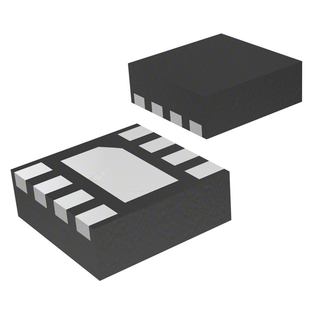
space saving, low profile 2.0 x 2.0 x 0.75 mm WDFN−8 package.
Features
•
•
•
•
•
•
•
•
•
•
•
•
•
•
•
2.3 V to 5.5 V Input Voltage Range
External Adjustable Voltage
Up to 1.2 A Output Current
3 MHz Switching Frequency
Synchronous Rectification
Automatic Power Save (NCP6332B) or External Mode Selection
(NCP6332C)
Enable Input
Power Good Output Option (NCP6332B)
Soft Start
Over Current Protection
Active Discharge When Disabled
Thermal Shutdown Protection
WDFN−8, 2 x 2 mm, 0.5 mm Pitch Package
Maximum 0.8mm Height for Super Thin Applications
This is a Pb−Free Device
MARKING
DIAGRAM
1
1
WDFN8
CASE 511BE
Ax
M
G
Ax MG
G
= Specific Device Code
= Date Code
= Pb−Free Package
(Note: Microdot may be in either location)
PINOUT
PGND
1
SW
2
8
PVIN
7
AVIN
9
AGND
3
6
MODE/PG
FB
4
5
EN
(Top View)
ORDERING INFORMATION
See detailed ordering, marking and shipping information in the
package dimensions section on page 2 of this data sheet.
Typical Applications
•
•
•
•
•
•
•
www.onsemi.com
Cellular Phones, Smart Phones, and PDAs
Portable Media Players
Digital Still Cameras
Wireless and DSL Modems
USB Powered Devices
Point of Load
Game and Entertainment System
© Semiconductor Components Industries, LLC, 2012
August, 2020 − Rev. 3
1
Publication Order Number:
NCP6332/D
�NCP6332B, NCP6332C
NCP6332B
1uH
Vo = 0.6V to Vin
Cout
10uF
Cfb
R1
Vin = 2.3V to 5.5V
PGND
PVIN
SW
AVIN
AGND
PG
FB
EN
Cin
10uF
Vo = 0.6V to Vin
Rpg
1M
Power Good
NCP6332C
1uH
Cout
10uF
Enable
Cfb
R1
PGND
PVIN
SW
AVIN
Cin
10uF
AGND MODE
FB
R2
Vin = 2.3V to 5.5V
Mode
Enable
EN
R2
(a) Power Good Output Option
(NCP6332B)
(b) External Mode Selection
(NCP6332C)
Figure 1. Typical Application Circuits
PIN DESCRIPTION
Pin
Name
Type
Description
1
PGND
Power
Ground
Power Ground for power, analog blocks. Must be connected to the system ground.
2
SW
Power
Output
Switch Power pin connects power transistors to one end of the inductor.
3
AGND
Analog
Ground
Analog Ground analog and digital blocks. Must be connected to the system ground.
4
FB
Analog
Input
Feedback Voltage from the buck converter output. This is the input to the error amplifier. This pin
is connected to the resistor divider network between the output and AGND.
5
EN
Digital
Input
Enable of the IC. High level at this pin enables the device. Low level at this pin disables the device.
6
PG/MODE
Digital
Output
PG pin is for NCP6332B with Power Good option. It is open drain output. Low level at this pin
indicates the device is not in power good, while high impedance at this pin indicates the device is
in power good.
MODE pin is for NCP6332C with mode external selection option. High level at this pin forces the
device to operate in forced PWM mode. Low level at this pin enables the device to operate in
automatic PFM/PWM mode for power saving function.
7
AVIN
Analog
Input
Analog Supply. This pin is the analog and the digital supply of the device. An optional 1 mF or larger ceramic capacitor bypasses this input to the ground. This capacitor should be placed as close
as possible to this input.
8
PVIN
Power
Input
Power Supply Input. This pin is the power supply of the device. A 10 mF or larger ceramic capacitor must bypass this input to the ground. This capacitor should be placed as close a possible to
this input.
9
PAD
Exposed
Pad
Exposed Pad. Must be soldered to system ground to achieve power dissipation performances.
This pin is internally unconnected
ORDERING INFORMATION
Marking
Package
Shipping†
NCP6332BMTAATBG**
AF
WDFN8
(Pb−Free)
3000 / Tape & Reel
NCP6332CMTAATBG*
AE
WDFN8
(Pb−Free)
3000 / Tape & Reel
Device
†For information on tape and reel specifications, including part orientation and tape sizes, please refer to our Tape and Reel Packaging
Specifications Brochure, BRD8011/D.
*Not recommended for new designs.
**This device is End of Life. Please contact sales for additional information and assistance with replacement devices.
www.onsemi.com
2
�NCP6332B, NCP6332C
Vin
Cin
PVIN
8
L
SW
2
Vo
1uH
Cout
10uF
10uF
AVIN
7
PWM / PFM
Control
UVLO
PGND
1
Cfb
R1
Enable
Power Good
EN
5
Rpg
1M
MODE/PG
6
MODE
PG
Logic Control
&
Current Limit
&
Thermal
Shutdown
FB
4
Error
Amp
R2
AGND
3
Reference
Voltage
Figure 2. Functional Block Diagram
MAXIMUM RATINGS
Value
Rating
Input Supply Voltage to GND
Switch Node to GND
EN, PG/MODE to GND
FB to GND
Symbol
Min
Max
Unit
VPVIN, VAVIN
−0.3
7.0
V
VSW
−0.3
7.0
V
VEN, VPG
−0.3
7.0
V
VFB
−0.3
2.5
V
Human Body Model (HBM) ESD Rating are (Note 1)
ESD HBM
2000
V
Machine Model (MM) ESD Rating (Note 1)
ESD MM
200
V
Latchup Current (Note 2)
ILU
−100
100
mA
Operating Junction Temperature Range (Note 3)
TJ
−40
125
°C
Operating Ambient Temperature Range
TA
−40
85
°C
Storage Temperature Range
TSTG
−55
150
°C
Thermal Resistance Junction−to−Top Case (Note 4)
RqJC
12
°C/W
Thermal Resistance Junction−to−Board (Note 4)
RqJB
30
°C/W
Thermal Resistance Junction−to−Ambient (Note 4)
RqJA
62
°C/W
PD
1.6
W
MSL
1
−
Power Dissipation (Note 5)
Moisture Sensitivity Level (Note 6)
Stresses exceeding those listed in the Maximum Ratings table may damage the device. If any of these limits are exceeded, device functionality
should not be assumed, damage may occur and reliability may be affected.
1. This device series contains ESD protection and passes the following tests:
Human Body Model (HBM) ±2.0 kV per JEDEC standard: JESD22−A114.
Machine Model (MM) ±200 V per JEDEC standard: JESD22−A115.
2. Latchup Current per JEDEC standard: JESD78 Class II.
3. The thermal shutdown set to 150°C (typical) avoids potential irreversible damage on the device due to power dissipation.
4. The thermal resistance values are dependent of the PCB heat dissipation. Board used to drive these data was an 80 x 50 mm NCP6332EVB
board. It is a multilayer board with 1 once internal power and ground planes and 2−once copper traces on top and bottom of the board. If
the copper trances of top and bottom are 1 once too, RqJC = 11°C/W, RqJB = 30°C/W, and RqJA = 72°C/W.
5. The maximum power dissipation (PD) is dependent on input voltage, maximum output current and external components selected.
6. Moisture Sensitivity Level (MSL): 1 per IPC/JEDEC standard: J−STD−020A.
www.onsemi.com
3
�NCP6332B, NCP6332C
ELECTRICAL CHARACTERISTICS (VIN = 3.6 V, VOUT = 1.8 V, L = 1 mH, C = 10 mF, typical values are referenced to TJ = 25°C, Min
and Max values are referenced to TJ up to 125°C, unless other noted.)
Symbol
Characteristics
Test Conditions
Min
Typ
Max
Unit
(Note 10)
2.3
−
5.5
V
EN high, no load, no switching, PFM Mode
EN high, no load, Forced PWM Mode
−
−
30
5
−
−
mA
mA
EN low
−
−
1
mA
(Note 7)
0.6
−
VIN
V
PWM Mode
594
600
606
mV
FB Voltage in Load Regulation
VIN = 3.6 V, IOUT from 200 mA to IOUTMAX,
PWM mode (Note 7)
−
−0.5
−
%/A
FB Voltage in Line Regulation
IOUT = 200 mA, VIN from MAX (VNOM +
0.5 V, 2.3 V) to 5.5 V, PWM mode (Note 7)
−
0
−
%/V
(Note 7)
−
100
−
%
(Note 7)
1.2
−
−
A
1.5
1.9
2.2
A
−
−
2.3
V
SUPPLY VOLTAGE
VIN
Input Voltage VIN Range
SUPPLY CURRENT
IQ
VIN Quiescent Supply Current
ISD
VIN Shutdown Current
OUTPUT VOLTAGE
VOUT
VFB
DMAX
Output Voltage Range
FB Voltage
Maximum Duty Cycle
OUTPUT CURRENT
IOUTMAX
Output Current Capability
ILIM
Output Peak Current Limit
VOLTAGE MONITOR
VINUV−
VIN UVLO Falling Threshold
VINHYS
VIN UVLO Hysteresis
VPGL
Power Good Low Threshold
60
−
200
mV
VOUT falls down to cross the threshold
(percentage of FB voltage) (Note 8)
87
90
92
%
VOUT rises up to cross the threshold
(percentage of Power Good Low Threshold
(VPGL) voltage) (Note 8)
0
3
5
%
VPGHYS
Power Good Hysteresis
TdPGH1
Power Good High Delay in Start Up
From EN rising edge to PG going high.
(Note 8)
−
1.15
−
ms
TdPGL1
Power Good Low Delay in Shut
Down
From EN falling edge to PG going low.
(Notes 7 and 8)
−
8
−
ms
TdPGH
Power Good High Delay in Regulation
From VFB going higher than 95% nominal
level to PG going high.
Not for the first time in start up. (Notes 7
and 8)
−
5
−
ms
TdPGL
Power Good Low Delay in Regulation
From VFB going lower than 90% nominal
level to PG going low. (Notes 7 and 8)
−
8
−
ms
VPG_L
Power Good Pin Low Voltage
Voltage at PG pin with 5 mA sink current
(Note 8)
−
−
0.3
V
PG_LK
Power Good Pin Leakage Current
3.6 V at PG pin when power good valid
(Note 8)
−
−
100
nA
INTEGRATED MOSFETs
RON_H
High−Side MOSFET ON Resistance
VIN = 3.6 V (Note 9)
VIN = 5 V (Note 9)
−
140
130
200
−
mW
RON_L
Low−Side MOSFET ON Resistance
VIN = 3.6 V (Note 9)
VIN = 5 V (Note 9)
−
110
100
140
−
mW
7. Guaranteed by design, not tested in production.
8. Power Good function is for NCP6332B devices only.
9. Maximum value applies for TJ = 85°C.
10. Operation above 5.5 V input voltage for extended periods may affect device reliability.
www.onsemi.com
4
�NCP6332B, NCP6332C
ELECTRICAL CHARACTERISTICS (VIN = 3.6 V, VOUT = 1.8 V, L = 1 mH, C = 10 mF, typical values are referenced to TJ = 25°C, Min
and Max values are referenced to TJ up to 125°C, unless other noted.)
Symbol
Characteristics
Test Conditions
Min
Typ
Max
Unit
2.7
3.0
3.3
MHz
−
0.4
1
ms
SWITCHING FREQUENCY
FSW
Normal Operation Frequency
SOFT START
TSS
Soft−Start Time
Time from EN to 90% of output voltage
target
CONTROL LOGIC
VEN_H
EN Input High Voltage
1.1
−
−
V
VEN_L
EN Input Low Voltage
−
−
0.4
V
VEN_HYS
EN Input Hysteresis
−
270
−
mV
IEN_BIAS
EN Input Bias Current
0.1
1
mA
VMODE_H
MODE Input High Voltage
(Note 11)
1.1
−
−
V
VMODE_L
MODE Input Low Voltage
(Note 11)
−
−
0.4
V
VMODE_HYS MODE Input Hysteresis
(Note 11)
−
270
−
mV
IMODE_BIAS MODE Input Bias Current
(Note 11)
0.1
1
mA
75
500
700
W
OUTPUT ACTIVE DISCHARGE
R_DIS
Internal Output Discharge Resistance
from SW to PGND
THERMAL SHUTDOWN
TSD
Thermal Shutdown Threshold
−
150
−
°C
TSD_HYS
Thermal Shutdown Hysteresis
−
25
−
°C
11. Mode function is for NCP6332C devices only.
www.onsemi.com
5
�NCP6332B, NCP6332C
TYPICAL OPERATING CHARACTERESTICS
1
Isd, Vin SHUTDOWN CURRENT (mA)
Isd, Vin SHUTDOWN CURRENT (mA)
1
0.9
0.8
0.7
0.6
0.5
0.4
0.3
0.2
0.1
0
2.5
3
3.5
4
4.5
5
0.9
0.8
0.7
0.6
0.5
0.4
0.3
0.2
0.1
0
−50
5.5
Figure 3. Standby Current vs. Input Voltage
(EN = Low, TA = 255C)
Iq, Vin QUIESCENT CURRENT (mA)
Iq, Vin QUIESCENT CURRENT (mA)
40
30
20
10
2.5
3
3.5
4
4.5
5
50
75
100
125
150
50
40
30
20
10
0
−50
5.5
−25
0
25
50
75
100
125
150
Vin, INPUT VOLTAGE (V)
TA, AMBIENT TEMPERATURE (°C)
Figure 5. Quiescent Current vs. Input Voltage
(EN = High, Open Loop, VOUT = 1.8 V,
TA = 255C)
Figure 6. Quiescent Current vs. Temperature
(EN = High, Open Loop, VOUT = 1.8 V,
VIN = 3.6 V)
100
100
95
95
Vin = 2.7 V
90
85
80
Vin = 5.5 V
75
Vin = 3.6 V
70
65
85
75
65
55
55
10000
Vin = 3.6 V
70
60
10
100
1000
Iout, OUTPUT CURRENT (mA)
Vin = 5.5 V
80
60
1
Vin = 2.7 V
90
EFFICIENCY (%)
EFFICIENCY (%)
25
60
50
50
0
Figure 4. Standby Current vs. Temperature
(EN = Low, VIN = 3.6 V)
60
0
−25
TA, AMBIENT TEMPERATURE (°C)
Vin, INPUT VOLTAGE (V)
50
1
Figure 7. Efficiency vs. Output Current and
Input Voltage (VOUT = 1.05 V, TA = 255C)
10
100
1000
Iout, OUTPUT CURRENT (mA)
Figure 8. Efficiency vs. Output Current and
Input Voltage (VOUT = 1.8 V, TA = 255C)
www.onsemi.com
6
10000
�NCP6332B, NCP6332C
TYPICAL OPERATING CHARACTERESTICS
100
100
95
90
EFFICIENCY (%)
EFFICIENCY (%)
90 Vin = 5.5 V
Vin = 5.5 V
85
80
75
70
65
85
80
75
70
65
60
60
55
55
50
1
Vin = 4.5 V
95
Vin = 3.6 V
10
100
1000
Iout, OUTPUT CURRENT (mA)
10000
50
1
Figure 9. Efficiency vs. Output Current and
Input Voltage (VOUT = 3.3 V, TA = 255C)
10000
Figure 10. Efficiency vs. Output Current and
Input Voltage (VOUT = 4 V , TA = 255C)
1.83
1.83
Vout, OUTPUT VOLTAGE (V)
Vin = 5.5 V
1.82
Vout, OUTPUT VOLTAGE (V)
10
100
1000
Iout, OUTPUT CURRENT (mA)
Vin = 3.6 V
1.81
1.8
1.79
Vin = 2.7 V
1.78
1.82
1.81
TA = 25°C
TA = −40°C
1.8
1.79
TA = 85°C
1.78
1.77
1.77
0
200
400
600
800
1000
1200
0
200
Iout, OUTPUT CURRENT (mA)
400
600
800
1000
Iout, OUTPUT CURRENT (mA)
Figure 11. Load Regulation vs. Output Current
and Input Voltage (VOUT = 1.8 V, TA = 255C)
Figure 12. Load Regulation vs. Output Current
and Temperature (VIN = 3.6 V, VOUT = 1.8 V).
VOUT
10 mV / Div
VOUT
5 mV / Div
25 mV
4 mV
SW
2 V / Div
SW
2 V / Div
Time: 5 ms / Div
Time: 500 ns / Div
Figure 14. Output Ripple Voltage in PFM Mode
(VIN = 3.6 V, VOUT = 1.8 V, IOUT = 10 mA, L=1 mH,
COUT = 10 mF)
Figure 13. Output Ripple Voltage in PWM Mode
(VIN = 3.6 V, VOUT = 1.8 V, IOUT = 1 A, L=1 mH,
COUT = 10 mF)
www.onsemi.com
7
1200
�NCP6332B, NCP6332C
TYPICAL OPERATING CHARACTERESTICS
VOUT 1.0 V / Div
VOUT 100 mV / Div
64 mV
60 mV
EN 5 V/ Div
1200 mA
200 mA
Iin 100 mA / Div
70 mA
IOUT 1 A / Div
SW 5 V / Div
SW 5 V / Div
Time 20 ms / Div
Time: 100 ms / Div
Figure 16. Power Up Sequence and Inrush Current in
Input (VIN = 3.6 V, VOUT = 1.8 V, IOUT = 0 A,
L = 1 mH, COUT = 10 mF)
Figure 15. Load Transient Response (VIN = 3.6 V,
VOUT = 1.8 V, IOUT = 200 mA to 1200 mA, L = 1 mH,
COUT = 10 mF)
VOUT 1.0 V / Div
VOUT 1.0 V / Div
EN 5 V/ Div
EN 5 V/ Div
PG 5 V / Div
PG 5 V / Div
SW 2 V / Div
SW 2 V / Div
Time: 200 ms / Div
Time: 1 ms / Div
Figure 18. Power Down Sequence and Active Output
Discharge (VIN = 3.6 V, VOUT = 1.8 V, IOUT = 0 A,
L = 1 mH, COUT = 10 mF)
Figure 17. Power Up Sequence and Power Good
(VIN = 3.6 V, VOUT = 1.8 V, IOUT = 0 A, L = 1 mH,
COUT = 10 mF)
www.onsemi.com
8
�NCP6332B, NCP6332C
DETAILED DESCRIPTION
General
PFM Mode Operation
The NCP6332B/C, a family of voltage−mode
synchronous buck converters, which is optimized to supply
different sub−systems of portable applications powered by
one cell Li−ion or three cell Alkaline/NiCd/NiMH batteries.
The devices are able to deliver up to 1.2 A on an external
adjustable voltage. Operation with 3 MHz switching
frequency allows employing small size inductor and
capacitors. Input supply voltage feedforward control is
employed to deal with wide input voltage range.
Synchronous rectification and automatic PWM/PFM power
save mode offer improved system efficiency.
In light load range, the inductor current becomes
discontinuous and the device automatically operates in PFM
mode with an adaptive fixed on time and variable switching
frequency. In this mode, the output voltage is regulated by
pulse frequency modulation of the internal P−MOSFET, and
the switching frequency is almost proportional to the
loading current. The internal N−MOSFET operates as
synchronous rectifier after each on pulse of the P−MOSFET
with a very small negative current limit. When the load
increases and the inductor current becomes continuous, the
controller automatically turns back to the fixed−frequency
PWM mode operation.
Operation Mode Selection (NCP6332C)
For NCP6332C with an external mode selection option,
high level (above 1.1 V) at MODE pin forces the device to
operate in forced PWM mode. Low level (below 0.4 V) at
this pin enables the device to operate in automatic
PFM/PWM mode for power saving function.
Undervoltage Lockout
PWM Mode Operation
Enable
In medium and heavy load range, the inductor current is
continuous and the device operates in PWM mode with fixed
switching frequency, which has a typical value of 3 MHz. In
this mode, the output voltage is regulated by on−time pulse
width modulation of an internal P−MOSFET. An internal
N−MOSFET operates as synchronous rectifier and its
turn−on signal is complimentary to that of the P−MOSFET.
The NCP6332B/C has an enable logic input pin EN. A
high level (above 1.1 V) on this pin enables the device to
active mode. A low level (below 0.4 V) on this pin disables
the device and makes the device in shutdown mode. There
is an internal filter with 5 ms time constant. The EN pin is
pulled down by an internal 10 nA sink current source. In
most of applications, the EN signal can be programmed
independently to VIN power sequence.
The input voltage VIN must reach or exceed 2.4 V
(typical) before the NCP6332B/C enables the converter
output to begin the start up sequence. The UVLO threshold
hysteresis is typically 100 mV.
1.1V
EN
0.4V
100us
95%
90%
300us
Vout
1.15ms
8us
5us
8us
PG
8us
Active
Discharge
Figure 19. Power Good and Active Discharge Timing Diagram
Power Good Output (NCP6332B)
power good signal is available. The power good signal is low
when EN is high but the output voltage has not been
established. Once the output voltage of the converter drops
out below 90% of its regulation during operation, the power
good signal is pulled low and indicates a power failure. A 5%
For NCP6332B with a power good output, the device
monitors the output voltage and provides a power good
output signal at the PG pin. This pin is an open−drain output
pin. To indicate the output of the converter is established, a
www.onsemi.com
9
�NCP6332B, NCP6332C
typical peak current limit ILMT is 1.6 A. If inductor current
exceeds the current limit threshold, the P−MOSFET will be
turned off cycle−by−cycle. The maximum output current
can be calculated by
hysteresis is required on power good comparator before
signal going high again.
Soft−Start
A soft start limits inrush current when the converter is
enabled. After a minimum 300 ms delay time following the
enable signal, the output voltage starts to ramp up in 100 ms
(for external adjustable voltage devices) or with a typical
10 V/ms slew rate (for fixed voltage devices).
I MAX + I LMT *
V OUT @ ǒV IN * V OUTǓ
2 @ V IN @ f SW @ L
(eq. 1)
where VIN is input supply voltage, VOUT is output voltage,
L is inductance of the filter inductor, and fSW is 3 MHz
normal switching frequency.
Active Output Discharge
An output discharge operation is active in when EN is low.
A discharge resistor (500 W typical) is enabled in this
condition to discharge the output capacitor through SW pin.
Thermal Shutdown
The NCP6332B/C has a thermal shutdown protection to
protect the device from overheating when the die
temperature exceeds 150°C. After the thermal protection is
triggered, the fault state can be ended by re−applying VIN
and/or EN when the temperature drops down below 125°C.
Cycle−by−Cycle Current Limitation
The NCP6332B/C protects the device from over current
with a fixed−value cycle−by−cycle current limitation. The
www.onsemi.com
10
�NCP6332B, NCP6332C
APPLICATION INFORMATION
Output Filter Design Considerations
to 50% of the maximum output current IOUT_MAX for a
trade−off between transient response and output ripple. The
inductance corresponding to the given current ripple is
The output filter introduces a double pole in the system at
a frequency of
f LC +
1
2 @ p @ ǸL @ C
(eq. 2)
L+
The internal compensation network design of the
NCP6332B/C is optimized for the typical output filter
comprised of a 1.0 mH inductor and a 10 mF ceramic output
capacitor, which has a double pole frequency at about
50 kHz. Other possible output filter combinations may have
a double pole around 50 kHz to have optimum operation
with the typical feedback network. Normal selection range
of the inductor is from 0.47 mH to 4.7 mH, and normal
selection range of the output capacitor is from 4.7 mF to
22 mF.
ǒVIN * VOUTǓ @ VOUT
(eq. 3)
V IN @ f SW @ I L_PP
The selected inductor must have high enough saturation
current rating to be higher than the maximum peak current
that is
I L_MAX + I OUT_MAX )
I L_PP
(eq. 4)
2
The inductor also needs to have high enough current
rating based on temperature rise concern. Low DCR is good
for efficiency improvement and temperature rise reduction.
Table 1 shows some recommended inductors for high power
applications and Table 2 shows some recommended
inductors for low power applications.
Inductor Selection
The inductance of the inductor is determined by given
peak−to−peak ripple current IL_PP of approximately 20%
Table 1. LIST OF RECOMMENDED INDUCTORS FOR HIGH POWER APPLICATIONS
Manufacturer
Part Number
Case Size
(mm)
L (mH)
Rated Current (mA)
(Inductance Drop)
Structure
MURATA
LQH44PN2R2MP0
4.0 x 4.0 x 1.8
2.2
2500 (−30%)
Wire Wound
MURATA
LQH44PN1R0NP0
4.0 x 4.0 x 1.8
1.0
2950 (−30%)
Wire Wound
MURATA
LQH32PNR47NNP0
3.0 x 2.5 x 1.7
0.47
3400 (−30%)
Wire Wound
Table 2. LIST OF RECOMMENDED INDUCTORS FOR LOW POWER APPLICATIONS
Manufacturer
Part Number
Case Size
(mm)
L (mH)
Rated Current (mA)
(Inductance Drop)
Structure
MURATA
LQH44PN2R2MJ0
4.0 x 4.0 x 1.1
2.2
1320 (−30%)
Wire Wound
MURATA
LQH44PN1R0NJ0
4.0 x 4.0 x 1.1
1.0
2000 (−30%)
Wire Wound
TDK
VLS201612ET−2R2
2.0 x 1.6 x 1.2
2.2
1150 (−30%)
Wire Wound
TDK
VLS201612ET−1R0
2.0 x 1.6 x 1.2
1.0
1650 (−30%)
Wire Wound
Output Capacitor Selection
operation mode, the three ripple components can be
obtained by
The output capacitor selection is determined by output
voltage ripple and load transient response requirement. For
a given peak−to−peak ripple current IL_PP in the inductor
of the output filter, the output voltage ripple across the
output capacitor is the sum of three ripple components as
below.
V OUT_PP(C) +
I L_PP
8 @ C @ f SW
V OUT_PP(ESR) + I L_PP @ ESR
V OUT_PP [ V OUT_PP(C) ) V OUT_PP(ESR) ) V OUT_PP(ESL)
V OUT_PP(ESL) +
(eq. 5)
ESL
ESL ) L
@ V IN
(eq. 6)
(eq. 7)
(eq. 8)
and the peak−to−peak ripple current is
where VOUT_PP(C) is a ripple component by an equivalent
total capacitance of the output capacitors, VOUT_PP(ESR)
is a ripple component by an equivalent ESR of the output
capacitors, and VOUT_PP(ESL) is a ripple component by
an equivalent ESL of the output capacitors. In PWM
I L_PP +
www.onsemi.com
11
ǒV IN * VOUTǓ @ VOUT
V IN @ f SW @ L
(eq. 9)
�NCP6332B, NCP6332C
In applications with all ceramic output capacitors, the
main ripple component of the output ripple is
VOUT_PP(C). So that the minimum output capacitance can
be calculated regarding to a given output ripple requirement
VOUT_PP in PWM operation mode.
C MIN +
I L_PP
8 @ V OUT_PP @ f SW
C IN_MIN +
I OUT_MAX @ ǒD * D 2Ǔ
V IN_PP @ f SW
(eq. 11)
where
D+
(eq. 10)
V OUT
(eq. 12)
V IN
In addition, the input capacitor needs to be able to absorb
the input current, which has a RMS value of
Input Capacitor Selection
I IN_RMS + I OUT_MAX @ ǸD * D 2
One of the input capacitor selection guides is the input
voltage ripple requirement. To minimize the input voltage
ripple and get better decoupling in the input power supply
rail, ceramic capacitor is recommended due to low ESR and
ESL. The minimum input capacitance regarding to the input
ripple voltage VIN_PP is
(eq. 13)
The input capacitor also needs to be sufficient to protect
the device from over voltage spike, and normally at least a
4.7 mF capacitor is required. The input capacitor should be
located as close as possible to the IC on PCB.
Table 3. LIST OF RECOMMENDED INPUT CAPACITORS AND OUTPUT CAPACITORS
Manufacturer
Part Number
Case
Size
C (mF)
Rated
Voltage
(V)
MURATA
GRM21BR60J226ME39, X5R
0805
1.4
22
6.3
MLCC
TDK
C2012X5R0J226M, X5R
0805
1.25
22
6.3
MLCC
MURATA
GRM21BR61A106KE19, X5R
0805
1.35
10
10
MLCC
TDK
C2012X5R1A106M, X5R
0805
1.25
10
10
MLCC
MURATA
GRM188R60J106ME47, X5R
0603
0.9
10
6.3
MLCC
TDK
C1608X5R0J106M, X5R
0603
0.8
10
6.3
MLCC
MURATA
GRM188R60J475KE19, X5R
0603
0.87
4.7
6.3
MLCC
Design of Feedback Network
ǒ
Ǔ
R1
R2
Structure
220 kW for applications with the typical output filter. R2 is
the resistance from FB to AGND, which is used to program
the output voltage according to equation (14) once the value
of R1 has been selected. A capacitor Cfb needs to be
employed between the VOUT and FB in order to provide
feedforward function to achieve optimum transient
response. Normal value range of Cfb is from 0 to 100 pF, and
a typical value is 15 pF for applications with the typical
output filter and R1 = 220 kW.
Table 4 provides reference values of R1 and Cfb in case
of different output filter combinations. The final design may
need to be fine tuned regarding to application specifications.
For NCP6332B/C devices with an external adjustable
output voltage, the output voltage is programmed by an
external resistor divider connected from VOUT to FB and
then to AGND, as shown in the typical application
schematic Figure 1(a). The programmed output voltage is
V OUT + V FB @ 1 )
Height
Max (mm)
(eq. 14)
where VFB is equal to the internal reference voltage 0.6 V,
R1 is the resistance from VOUT to FB, which has a normal
value range from 50 kW to 1 MW and a typical value of
Table 4. Reference Values of Feedback Networks (R1 and Cfb) for Output Filter Combinations (L and C)
R1 (kW)
L (mH)
Cfb (pF)
4.7
C (mF)
10
22
0.47
0.68
1
2.2
3.3
4.7
220
220
220
220
330
330
3
5
8
15
15
22
220
220
220
220
330
330
8
10
15
27
27
39
220
220
220
220
330
330
15
22
27
39
47
56
www.onsemi.com
12
�NCP6332B, NCP6332C
LAYOUT CONSIDERATIONS
• Arrange a “quiet” path for output voltage sense and
Electrical Layout Considerations
Good electrical layout is a key to make sure proper
operation, high efficiency, and noise reduction. Electrical
layout guidelines are:
• Use wide and short traces for power paths (such as
PVIN, VOUT, SW, and PGND) to reduce parasitic
inductance and high−frequency loop area. It is also
good for efficiency improvement.
• The device should be well decoupled by input capacitor
and input loop area should be as small as possible to
reduce parasitic inductance, input voltage spike, and
noise emission.
• SW node should be a large copper pour, but compact
because it is also a noise source.
• It would be good to have separated ground planes for
PGND and AGND and connect the two planes at one
point. Directly connect AGND pin to the exposed pad
and then connect to AGND ground plane through vias.
Try best to avoid overlap of input ground loop and
output ground loop to prevent noise impact on output
regulation.
feedback network, and make it surrounded by a ground
plane.
Thermal Layout Considerations
Good thermal layout helps high power dissipation from a
small package with reduced temperature rise. Thermal
layout guidelines are:
• The exposed pad must be well soldered on the board.
• A four or more layers PCB board with solid ground
planes is preferred for better heat dissipation.
• More free vias are welcome to be around IC and/or
underneath the exposed pad to connect the inner ground
layers to reduce thermal impedance.
• Use large area copper especially in top layer to help
thermal conduction and radiation.
• Do not put the inductor to be too close to the IC, thus
the heat sources are distributed.
GND
VIN
P
P
P
P
Cin
P
L
ÏÏÏÏÏÏÏÏÏÏ
ÏÏÏÏÏÏÏÏÏÏ
ÏÏÏÏÏÏÏÏÏÏ
ÏÏÏÏÏÏÏÏÏÏ
ÎÎÎ
ÎÎÎ
ÎÎÎ
ÏÏÏ
ÏÏÏ
ÏÏÏ
PGND
1
SW
2
AGND
F
FB
A
A
3
4
A
ÏÏÏ
ÏÏÏ
ÏÏÏ
ÏÏÏ
ÎÎÎ
ÎÎÎ
8
PVIN
7
AVIN
6
MODE/PG
5
EN
P
Cout
ÎÎÎÎÎÎÎÎÎÎ
ÎÎÎÎÎÎÎÎÎÎ
ÎÎÎÎÎÎÎÎÎÎ
ÎÎÎÎÎÎÎÎÎÎ
P
P
P
O
P
P
P
P
P
P
Cfb
F
R1
R2
VOUT
GND
Figure 20. Recommended PCB Layout for Application Boards
www.onsemi.com
13
O
A
�MECHANICAL CASE OUTLINE
PACKAGE DIMENSIONS
WDFN8 2x2, 0.5P
CASE 511BE−01
ISSUE A
1
DATE 27 MAY 2011
SCALE 2:1
A
D
PIN ONE
REFERENCE
2X
0.10 C
2X
E
DETAIL A
ALTERNATE
CONSTRUCTIONS
TOP VIEW
ÇÇÇ
ÉÉÉ
ÉÉÉ
EXPOSED Cu
DETAIL B
A
0.10 C
A3
MOLD CMPD
0.08 C
ALTERNATE
CONSTRUCTIONS
A1
SIDE VIEW
C
D2
DETAIL A
1
8X
4
SEATING
PLANE
K
5
e
L
1
8X
MILLIMETERS
MIN
MAX
0.70
0.80
0.00
0.05
0.20 REF
0.20
0.30
2.00 BSC
1.50
1.70
2.00 BSC
0.80
1.00
0.50 BSC
0.25 REF
0.20
0.40
−−−
0.15
XX MG
G
XX = Specific Device Code
M = Date Code
G
= Pb−Free Package
b
0.10 C A B
BOTTOM VIEW
0.05 C
(Note: Microdot may be in either location)
*This information is generic. Please refer to
device data sheet for actual part marking.
Pb−Free indicator, “G” or microdot “ G”,
may or may not be present.
NOTE 3
RECOMMENDED
SOLDERING FOOTPRINT*
8X
1.70
PACKAGE
OUTLINE
A3
DIM
A
A1
A3
b
D
D2
E
E2
e
K
L
L1
GENERIC
MARKING DIAGRAM*
E2
8
ÇÇ
ÉÉ
A1
DETAIL B
NOTE 4
NOTES:
1. DIMENSIONING AND TOLERANCING PER
ASME Y14.5M, 1994.
2. CONTROLLING DIMENSION: MILLIMETERS.
3. DIMENSION b APPLIES TO PLATED
TERMINAL AND IS MEASURED BETWEEN
0.15 AND 0.30 MM FROM TERMINAL TIP.
4. COPLANARITY APPLIES TO THE EXPOSED
PAD AS WELL AS THE TERMINALS.
L1
ÇÇ
ÇÇ
ÇÇ
0.10 C
L
L
B
0.50
2.30
1.00
1
0.50
PITCH
8X
0.30
DIMENSIONS: MILLIMETERS
*For additional information on our Pb−Free strategy and soldering
details, please download the ON Semiconductor Soldering and
Mounting Techniques Reference Manual, SOLDERRM/D.
DOCUMENT NUMBER:
DESCRIPTION:
98AON48936E
WDFN8, 2X2, 0.5P
Electronic versions are uncontrolled except when accessed directly from the Document Repository.
Printed versions are uncontrolled except when stamped “CONTROLLED COPY” in red.
PAGE 1 OF 1
ON Semiconductor and
are trademarks of Semiconductor Components Industries, LLC dba ON Semiconductor or its subsidiaries in the United States and/or other countries.
ON Semiconductor reserves the right to make changes without further notice to any products herein. ON Semiconductor makes no warranty, representation or guarantee regarding
the suitability of its products for any particular purpose, nor does ON Semiconductor assume any liability arising out of the application or use of any product or circuit, and specifically
disclaims any and all liability, including without limitation special, consequential or incidental damages. ON Semiconductor does not convey any license under its patent rights nor the
rights of others.
© Semiconductor Components Industries, LLC, 2019
www.onsemi.com
�onsemi,
, and other names, marks, and brands are registered and/or common law trademarks of Semiconductor Components Industries, LLC dba “onsemi” or its affiliates
and/or subsidiaries in the United States and/or other countries. onsemi owns the rights to a number of patents, trademarks, copyrights, trade secrets, and other intellectual property.
A listing of onsemi’s product/patent coverage may be accessed at www.onsemi.com/site/pdf/Patent−Marking.pdf. onsemi reserves the right to make changes at any time to any
products or information herein, without notice. The information herein is provided “as−is” and onsemi makes no warranty, representation or guarantee regarding the accuracy of the
information, product features, availability, functionality, or suitability of its products for any particular purpose, nor does onsemi assume any liability arising out of the application or use
of any product or circuit, and specifically disclaims any and all liability, including without limitation special, consequential or incidental damages. Buyer is responsible for its products
and applications using onsemi products, including compliance with all laws, regulations and safety requirements or standards, regardless of any support or applications information
provided by onsemi. “Typical” parameters which may be provided in onsemi data sheets and/or specifications can and do vary in different applications and actual performance may
vary over time. All operating parameters, including “Typicals” must be validated for each customer application by customer’s technical experts. onsemi does not convey any license
under any of its intellectual property rights nor the rights of others. onsemi products are not designed, intended, or authorized for use as a critical component in life support systems
or any FDA Class 3 medical devices or medical devices with a same or similar classification in a foreign jurisdiction or any devices intended for implantation in the human body. Should
Buyer purchase or use onsemi products for any such unintended or unauthorized application, Buyer shall indemnify and hold onsemi and its officers, employees, subsidiaries, affiliates,
and distributors harmless against all claims, costs, damages, and expenses, and reasonable attorney fees arising out of, directly or indirectly, any claim of personal injury or death
associated with such unintended or unauthorized use, even if such claim alleges that onsemi was negligent regarding the design or manufacture of the part. onsemi is an Equal
Opportunity/Affirmative Action Employer. This literature is subject to all applicable copyright laws and is not for resale in any manner.
PUBLICATION ORDERING INFORMATION
LITERATURE FULFILLMENT:
Email Requests to: orderlit@onsemi.com
onsemi Website: www.onsemi.com
◊
TECHNICAL SUPPORT
North American Technical Support:
Voice Mail: 1 800−282−9855 Toll Free USA/Canada
Phone: 011 421 33 790 2910
Europe, Middle East and Africa Technical Support:
Phone: 00421 33 790 2910
For additional information, please contact your local Sales Representative
�


 工商网监
湘ICP备2023018690号
工商网监
湘ICP备2023018690号
