NCP81152
Synchronous Buck Dual
MOSFET Driver
The NCP81152 is a high−performance dual MOSFET gate driver
optimized to drive the gates of both high−side and low−side power
MOSFETs in a synchronous buck converter. Two drivers are
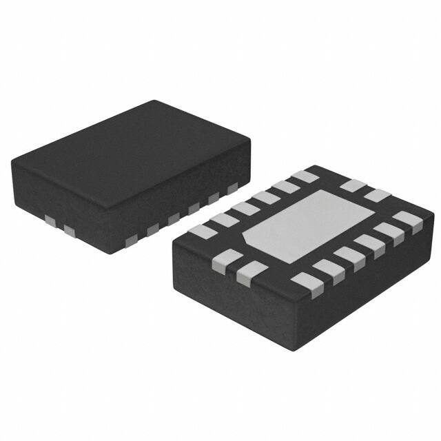
co−packaged into a 2.5 mm x 3.5 mm QFN16 package that greatly
reduces the footprint compared to two discrete drivers. Adaptive
anti−cross−conduction circuitry and power saving operation provides
a low−switching−loss and high−efficiency solution for notebook
systems. The under−voltage lockout function guarantees the outputs
are low when the supply voltage is low.
www.onsemi.com
1
QFN16
MN SUFFIX
CASE 485AW
Features
•
•
•
•
•
•
•
•
•
Adaptive Anti−Cross−Conduction Circuit
Integrated Bootstrap Diode
Zero Cross Detection
Floating Top Driver Accommodates Boost Voltages up to 35 V
Output Disable Control Turns Off Both MOSFETs
Under−voltage Lockout
Power Saving Operation Under Light Load Conditions
Thermally Enhanced Package
These are Pb−Free Devices
Typical Applications
• Vcore Power for Notebook Systems
• Power Systems for DDR and Graphics
MARKING DIAGRAM
81152
ALYWG
G
81152 = Specific Device Code
A
= Assembly Location
L
= Wafer Lot
Y
= Year
W
= Work Week
G
= Pb−Free Package
(Note: Microdot may be in either location)
BST1
DRVH1
PIN CONNECTIONS
16
FLAG
1
SW1
GND1
DRVL1
DRVH2
SW2
GND2
VCC2
DRVL2
PWM1
EN1
VCC1
BST2
PWM2
EN2
(Top View)
ORDERING INFORMATION
Device
Package
Shipping†
NCP81152MNTWG
QFN16
(Pb−Free)
3000 / Tape &
Reel
†For information on tape and reel specifications,
including part orientation and tape sizes, please
refer to our Tape and Reel Packaging Specifications
Brochure, BRD8011/D.
© Semiconductor Components Industries, LLC, 2015
January, 2015 − Rev. 2
1
Publication Order Number:
NCP81152/D
�NCP81152
BST1
VCC1
DRVH1
PWM1
Logic
SW1
Anti−Cross
Conduction
VCC1
DRVL1
EN1
Zero
Cross
Detection
UVLO
VCC2
BST2
DRVH2
PWM2
Logic
SW2
Anti−Cross
Conduction
VCC2
DRVL2
Zero
Cross
Detection
EN2
UVLO
Figure 1. Block Diagram
www.onsemi.com
2
�NCP81152
Table 1. PIN DESCRIPTIONS
Pin No.
Symbol
Description
1, 5
BST1, BST2
Floating bootstrap supply pin for high−side gate driver. Connect the bootstrap capacitor between this pin
and the SW pin.
2, 6
PWM1, PWM2
3, 7
EN1, EN2
4, 8
VCC1, VCC2
9, 13
DRVL1, DRVL2
10, 14
GND1, GND2
11, 15
SW1, SW2
12, 16
DRVH1, DRVH2
17
FLAG
Control input. The PWM signal has three states:
PWM = High enables the high−side FET;
PWM = Mid enables zero cross detection;
PWM = Low enables the low−side FET.
Logic input. Three−state logic input:
EN = High enables the driver;
EN = Mid goes into diode braking mode (both high−side and low−side gate drive signals are low);
EN = Low disables the driver.
Power supply input. Connect a bypass capacitor (0.1 mF) from this pin to ground.
Low−side gate drive output. Connect to the gate of the low−side MOSFET.
Bias and reference ground. All signals are referenced to this node.
Switch node. Connect this pin to the source of the high−side MOSFET and drain of the low−side MOSFET.
High−side gate drive output. Connect to the gate of the high−side MOSFET.
Thermal flag. There is no electrical connection to the IC. Connect to ground plane.
Table 2. ABSOLUTE MAXIMUM RATINGS
Pin Symbol
Pin Name
VMAX
VMIN
VCC1, VCC2
Main Supply Voltage Input
6.5 V
−0.3 V
BST1, BST2
Bootstrap Supply Voltage
35 V wrt/ GND
40 V ≤ 50 ns wrt/ GND
6.5 V wrt/ SW
−0.3 V wrt/SW
SW1, SW2
Switching Node
(Bootstrap Supply Return)
35 V
40 V ≤ 50 ns
−5 V
−10 V (200 ns)
DRVH1, DRVH2
High Side Driver Output
BST+0.3 V
−0.3 V wrt/SW
−2 V (
很抱歉,暂时无法提供与“NCP81152MNTWG”相匹配的价格&库存,您可以联系我们找货
免费人工找货- 国内价格 香港价格
- 1+2.212661+0.26820
- 10+2.1777510+0.26397
- 25+2.1428425+0.25974
- 100+2.10672100+0.25536
- 250+2.07181250+0.25113
- 国内价格
- 10+1.85610
- 25+1.72477
- 100+1.53216
- 250+1.50677


 工商网监
湘ICP备2023018690号
工商网监
湘ICP备2023018690号
