NCV4274, NCV4274A
Regulator Family,
400 mA, 2% and 4% Voltage
Description
The NCV4274 and NCV4274A is a precision micro−power voltage
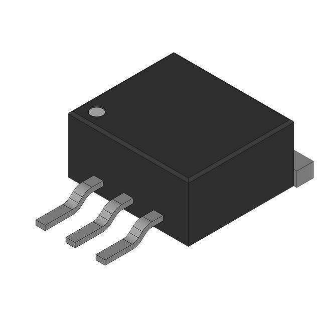
regulator with an output current capability of 400 mA available in the
DPAK, D2PAK and SOT−223 packages.
The output voltage is accurate within ±2.0% or ±4.0% depending on
the version with a maximum dropout voltage of 0.5 V with an input up
to 40 V. Low quiescent current is a feature drawing only 150 mA with a
1 mA load. This part is ideal for automotive and all battery operated
microprocessor equipment.
The regulator is protected against reverse battery, short circuit, and
thermal overload conditions. The device can withstand load dump
transients making it suitable for use in automotive environments.
www.onsemi.com
MARKING DIAGRAMS
4
74X−xxG
ALYWW
x
DPAK
DT SUFFIX
CASE 369C
1
Features
•
•
•
•
•
•
•
•
•
2.5, 3.3 V, 5.0 V, 8.5 V, ±2.0% Output Options
2.5, 3.3 V, 5.0 V, ±4.0% Output Options
Low 150 mA Quiescent Current at 1 mA load current
400 mA Output Current Capability
Fault Protection
+60 V Peak Transient Voltage with Respect to GND
S −42 V Reverse Voltage
S Short Circuit
S Thermal Overload
Very Low Dropout Voltage
NCV Prefix for Automotive and Other Applications Requiring
Unique Site and Control Change Requirements; AEC−Q100
Qualified and PPAP Capable
These are Pb−Free Devices
2
1
Input
2, 4 Ground
3
Output
3
4
D2PAK
DS SUFFIX
CASE 418AF
NC
V4274X−xx
AWLYWWG
1
2
1
Input
2, 4 Ground
3
Output
3
4
SOT−223
ST SUFFIX
CASE 318E
AYW
74X−xxG
G
1
2
1
Input
2, 4 Ground
3
Output
3
X
= A or blank
xx
= Voltage Ratings
A
= Assembly Location
L, WL = Wafer Lot
Y
= Year
WW, W = Work Week
G, G
= Pb−Free Package
(Note: Microdot may be in either location)
ORDERING INFORMATION
See detailed ordering and shipping information in the package
dimensions section on page 15 of this data sheet.
© Semiconductor Components Industries, LLC, 2013
November, 2018 − Rev. 16
1
Publication Order Number:
NCV4274/D
�NCV4274, NCV4274A
I
Q
Bandgap
Refernece
Current Limit and
Saturation Sense
−
+
Thermal
Shutdown
GND
Figure 1. Block Diagram
Pin Definitions and Functions
Pin No.
Symbol
1
I
2,4
GND
3
Q
Function
Input; Bypass directly at the IC a ceramic capacitor to GND.
Ground
Output; Bypass with a capacitor to GND.
1. DPAK 3LD package code 6025
2. D2PAK 3LD package code 6083
ABSOLUTE MAXIMUM RATINGS
Pin Symbol, Parameter
I, Input−to−Regulator
Symbol
Condition
Min
Max
Unit
V
Voltage
VI
−42
45
Current
II
Internally
Limited
Internally
Limited
I, Input peak Transient Voltage to Regulator with Respect
to GND
VI
60
V
Q, Regulated Output
Voltage
VQ
−1.0
40
V
Current
IQ
Internally
Limited
Internally
Limited
GND, Ground Current
IGND
−
100
mA
Junction Temperature
Storage Temperature
TJ
TStg
−
−50
150
150
°C
°C
ESD Capability, Human Body Model
ESDHB
4
kV
ESD Capability, Machine Model
ESDMM
200
V
ESD Capability, Charged Device Model
ESDCDM
1
kV
VQ = VI
Stresses exceeding those listed in the Maximum Ratings table may damage the device. If any of these limits are exceeded, device functionality
should not be assumed, damage may occur and reliability may be affected.
3. This device series incorporates ESD protection and is tested by the following methods:
ESD HBM tested per AEC−Q100−002 (EIA/JESD22−A114)
ESD MM tested per AEC−Q100−003 (EIA/JESD22−A115)
ESD CDM tested per EIA/JES D22/C101, Field Induced Charge Model
www.onsemi.com
2
�NCV4274, NCV4274A
OPERATING RANGE
Min
Max
Unit
Input Voltage (8.5 V Version)
Parameter
Symbol
VI
Condition
9.0
40
V
Input Voltage (5.0 V Version)
VI
5.5
40
V
Input Voltage (3.3 V, and 2.5 V Version)
VI
4.5
40
V
Junction Temperature
TJ
−40
150
°C
THERMAL RESISTANCE
Min
Max
Unit
Junction−to−Ambient
Parameter
DPAK
Rthja
−
70
(Note 4)
°C/W
Junction−to−Ambient
D2PAK
Rthja
−
60
(Note 4)
°C/W
Junction−to−Case
DPAK
Rthjc
−
4
°C/W
D2PAK
Rthjc
−
3
°C/W
Y−JLX,
−
14.5
(Note 5)
°C/W
−
169.7
(Note 5)
°C/W
Unit
Junction−to−Case
Junction−to−Tab
Symbol
SOT−223
Condition
YLX
Junction−to−Ambient
SOT−223
RqJA, qJA
4. Soldered in, minimal footprint, FR4
5. 1 oz copper, 5 mm2 copper area, FR4
LEAD FREE SOLDERING TEMPERATURE AND MSL
Parameter
Lead Free Soldering, (Note 6)
Reflow (SMD styles only),
Moisture Sensitivity Level
Pb−Free
Symbol
Condition
Min
Max
Tsld
60s − 150s Above 217s
40s Max at Peak
−
265 pk
MSL
DPAK and D2PAK
SOT−223
1
3
−
−
6. Per IPC/JEDEC J−STD−020C
www.onsemi.com
3
°C
�NCV4274, NCV4274A
ELECTRICAL CHARACTERISTICS
−40°C < TJ < 150°C; VI = 13.5 V unless otherwise noted.
Min
Parameter
Symbol
Typ
Max
Min
NCV4274A
Test Conditions
Typ
Max
NCV4274
Unit
REGULATOR
Output Voltage (8.5 V Version)
VQ
5 mA < IQ < 200 mA
9.5 V < VI < 40 V
8.33
8.5
8.67
−
−
−
V
Output Voltage (8.5 V Version)
VQ
5 mA < IQ < 400 mA
9.5 V < VI < 28 V
8.33
8.5
8.67
−
−
−
V
Output Voltage (5.0 V Version)
VQ
5 mA < IQ < 400 mA
6 V < VI < 28 V
4.9
5.0
5.1
4.8
5.0
5.2
V
Output Voltage (5.0 V Version)
VQ
5 mA < IQ < 200 mA
6 V < VI < 40 V
4.9
5.0
5.1
4.8
5.0
5.2
V
Output Voltage (3.3 V Version)
VQ
5 mA < IQ < 400 mA
4.5 V < VI < 28 V
3.23
3.3
3.37
3.17
3.3
3.43
V
Output Voltage (3.3 V Version)
VQ
5 mA < IQ < 200 mA
4.5 V < VI < 40 V
3.23
3.3
3.37
3.17
3.3
3.43
V
Output Voltage (2.5 V Version)
VQ
5 mA < IQ < 400 mA
4.5 V < VI < 28 V
2.45
2.5
2.55
2.4
2.5
2.6
V
Output Voltage (2.5 V Version)
VQ
5 mA < IQ < 200 mA
4.5 V < VI < 40 V
2.45
2.5
2.55
2.4
2.5
2.6
V
Current Limit
IQ
−
400
600
−
400
600
−
mA
Quiescent Current
Iq
IQ = 1 mA
VQ = 8.5 V
VQ = 5.0 V
VQ = 3.3 V
VQ = 2.5 V
IQ = 250 mA
VQ = 8.5 V
VQ = 5.0 V
VQ = 3.3 V
VQ = 2.5 V
IQ = 400 mA
VQ = 8.5 V
VQ = 5.0 V
VQ = 3.3 V
VQ = 2.5 V
−
−
−
−
195
190
145
140
250
250
250
250
−
−
−
−
−
190
145
140
−
250
250
250
mA
mA
mA
mA
−
−
−
−
10
10
13
12
15
15
20
20
−
−
−
−
−
10
13
12
−
15
20
20
mA
mA
mA
mA
−
−
−
−
20
20
30
28
35
35
45
45
−
−
−
−
−
20
30
28
−
35
45
45
mA
mA
mA
mA
IQ = 250 mA,
VDR = VI − VQ
VI = 8.5 V
VI = 5.0 V
VI = 4.5 V
VI = 4.5 V
−
−
−
−
250
250
−
−
500
500
1.27
2.05
−
−
−
−
−
250
−
−
−
500
1.33
2.1
mV
mV
V
V
Dropout Voltage
VDR
8.5 V Version
5.0 V Version
3.3 V Version
2.5 V Version
Load Regulation
DVQ
IQ = 5 mA to 400 mA
−
7
20
−
7
30
mV
Line Regulation
DVQ
DVI = 12 V to 32 V
IQ = 5 mA
−
10
25
−
10
25
mV
Power Supply Ripple Rejection
PSRR
ƒr = 100 Hz,
Vr = 0.5 VPP
−
60
−
−
60
−
dB
Temperature output voltage drift
DVQ/DT
−
0.5
−
−
0.5
−
mV/K
Thermal Shutdown Temperature*
TSD
165
−
210
165
−
210
°C
IQ = 5 mA
*Guaranteed by design, not tested in production
www.onsemi.com
4
�NCV4274, NCV4274A
VI
II
I
C12
100 nF
C11
1.0 mF
VI
1
Q
NCV4274 3
NCV4274A
CQ
10 mF
or
22 mF
2,4
GND
IGND
VQ
IQ
VQ
VI
CI
100 nF
Input
Rload
1
NCV4274 3
NCV4274A
VQ
CQ*
Output
2,4
GND
*CQ = 10 mF for VQ ≤ 3.3 V
CQ = 22 mF for VQ ≥ 5 V
Figure 2. Measuring Circuit
Figure 3. Application Circuit
TYPICAL CHARACTERISTIC CURVES
100
1000
VI = 13.5 V
100
Maximum ESR
COUT = 10 mF − 100 mF
ESR (W)
ESR (W)
10
VI = 13.5 V
1
0.1
0.01
50
100
150
200
250
Stable Region
1.0
Stable Region
0
Maximum ESR
COUT = 1 mF − 100 mF
10
300
350
0.1
400
Minimum ESR
COUT = 1 mF
0
LOAD CURRENT (mA)
5
20
60 100 140 180 220 260 300 340 380 420
LOAD CURRENT (mA)
Figure 4. ESR Characterization − 3.3 V, 5 V and
8.5 V Versions
Figure 5. ESR Characterization − 2.5 V Version
www.onsemi.com
5
�NCV4274, NCV4274A
TYPICAL CHARACTERISTIC CURVES − 8.5 V Version
10
8.7
VI = 13.5 V
RL = 1.7 kW
8
8.6
7
VQ (V)
VQ (V)
RL = 33 W
TJ = 25°C
9
8.5
6
5
4
3
8.4
2
1
0
8.3
−40
0
40
80
120
0
160
TJ (°C)
2
4
6
8
10
VI (V)
Figure 6. Output Voltage vs. Junction Temperature
Figure 7. Output Voltage vs. Input Voltage
35
1000
TJ = 25°C
VQ = 0 V
800
TJ = 25°C
VI = 13.5 V
30
600
Iq (mA)
IQ (mA)
25
400
20
15
10
200
0
5
0
10
20
30
40
0
50
0
100
200
300
400
500
IQ (mA)
VI (V)
Figure 8. Output Current vs. Input Voltage
Figure 9. Current Consumption vs. Output
Current (High Load)
1.6
600
VI = 13.5 V
TJ = 25°C
VI = 13.5 V
1.4
500
1.2
400
VDR (mV)
Iq (mA)
1
0.8
0.6
TJ = 125°C
300
TJ = 25°C
200
0.4
100
0.2
0
0
10
20
30
40
50
0
60
0
100
200
300
IQ (mA)
IQ (mA)
Figure 10. Current Consumption vs. Output
Current (Low Load)
Figure 11. Drop Voltage vs. Output Current
www.onsemi.com
6
400
�NCV4274, NCV4274A
TYPICAL CHARACTERISTIC CURVES − 8.5 V Version
6
50
RL = 33 W
TJ = 25°C
40
4
2
RL = 6.8 kW
TJ = 25°C
−2
30
II (mA)
Iq (mA)
0
20
−4
−6
−8
−10
10
−12
−14
0
0
10
20
30
40
−16
−50
50
VI (V)
−30
−10
10
30
VI (V)
Figure 12. Current Consumption vs. Input Voltage
Figure 13. Input Current vs. Input Voltage
www.onsemi.com
7
50
�NCV4274, NCV4274A
TYPICAL CHARACTERISTIC CURVES − 5.0 V Version
5.2
6
VI = 13.5 V
RL = 1 kW
RL = 20 W
TJ = 25°C
5
5.1
VQ (V)
VQ (V)
4
5.0
3
2
4.9
1
0
4.8
−40
0
40
80
120
160
0
TJ (°C)
2
4
6
8
10
VI (V)
Figure 14. Output Voltage vs. Junction
Temperature
Figure 15. Output Voltage vs. Input Voltage
60
800
TJ = 25°C
VQ = 0 V
TJ = 25°C
VI = 13.5 V
50
600
Iq (mA)
IQ (mA)
40
400
30
20
200
10
0
0
0
10
20
30
40
0
50
100
200
300
IQ (mA)
VI (V)
Figure 16. Output Current vs. Input Voltage
1.2
600
600
TJ = 25°C
VI = 13.5 V
500
400
VDR (mV)
1
Iq (mA)
500
Figure 17. Current Consumption vs. Output
Current (High Load)
1.6
1.4
400
0.8
0.6
TJ = 125°C
300
TJ = 25°C
200
0.4
100
0.2
0
0
10
20
30
40
50
0
60
0
100
200
300
IQ (mA)
IQ (mA)
Figure 18. Current Consumption vs. Output
Current (Low Load)
Figure 19. Drop Voltage vs. Output Current
www.onsemi.com
8
400
�NCV4274, NCV4274A
TYPICAL CHARACTERISTIC CURVES − 5.0 V Version
6
40
4
RL = 20 W
TJ = 25°C
2
30
RL = 6.8 kW
TJ = 25°C
0
II (mA)
Iq (mA)
−2
20
−4
−6
−8
−10
10
−12
−14
0
0
10
20
30
40
−16
−50
50
VI (V)
−25
0
25
VI (V)
Figure 20. Current Consumption vs. Input Voltage
Figure 21. Input Current vs. Input Voltage
www.onsemi.com
9
50
�NCV4274, NCV4274A
TYPICAL CHARACTERISTIC CURVES − 3.3 V Version
3.5
6
VI = 6 V
RL = 1 kW
3.4
4
VQ (V)
3.3
VQ (V)
RL = 20 W
TJ = 25°C
5
3.2
3
3.1
2
3.0
1
2.9
−40
0
0
40
80
120
160
0
TJ (°C)
2
1
3
4
5
6
VI (V)
Figure 22. Output Voltage vs. Junction
Temperature
Figure 23. Output Voltage vs. Input Voltage
800
60
TJ = 25°C
VQ = 0 V
TJ = 25°C
VI = 13.5 V
50
600
Iq (mA)
IQ (mA)
40
400
30
20
200
10
0
0
10
20
30
40
0
50
0
100
200
VI (V)
Figure 24. Output Current vs. Input Voltage
500
600
1.26
TJ = 25°C
VI = 13.5 V
1.4
1.24
1.2
TJ = 125°C
1.22
VDR (V)
1.0
Iq (mA)
400
Figure 25. Current Consumption vs. Output
Current (High Load)
1.6
0.8
0.6
TJ = 25°C
1.20
1.18
VDR = VI(min) − VQ
0.4
1.16
0.2
0
300
IQ (mA)
0
10
20
30
40
50
60
1.14
0
100
200
300
IQ (mA)
IQ (mA)
Figure 26. Current Consumption vs. Output
Current (Low Load)
Figure 27. Voltage Drop vs. Output Current
www.onsemi.com
10
400
�NCV4274, NCV4274A
TYPICAL CHARACTERISTIC CURVES − 3.3 V Version
7
4
2
RL = 20 W
TJ = 25°C
6
0
−2
4
II (mA)
Iq (mA)
5
3
−6
−8
−10
2
−12
1
0
−4
RL = 3.3 kW
TJ = 25°C
−14
0
10
20
30
40
−16
−50
50
VI (V)
−25
0
25
VI (V)
Figure 28. Current Consumption vs. Input Voltage
Figure 29. Input Current vs. Input Voltage
www.onsemi.com
11
50
�NCV4274, NCV4274A
TYPICAL CHARACTERISTIC CURVES − 2.5 V Version
2.7
5.0
4.5
VI = 6 V
RL = 1 kW
2.6
4.0
3.5
VQ (V)
VQ (V)
2.5
2.4
2.3
3.0
2.5
2.0
1.5
1.0
2.2
0.5
2.1
−40
0
0
40
80
120
160
0
1
2
TJ (°C)
3
4
5
6
VI (V)
Figure 30. Output Voltage vs. Junction
Temperature
Figure 31. Output Voltage vs. Input Voltage
800
60
TJ = 25°C
VQ = 0 V
TJ = 25°C
VI = 13.5 V
50
600
Iq (mA)
IQ (mA)
40
400
30
20
200
10
0
0
10
20
30
40
0
50
0
100
200
VI (V)
Figure 32. Output Current vs. Input Voltage
500
600
2.05
TJ = 25°C
VI = 13.5 V
1.4
2.04
2.03
1.2
2.02
1.0
TJ = 125°C
2.01
VDR (V)
Iq (mA)
400
Figure 33. Current Consumption vs. Output
Current (High Load)
1.6
0.8
0.6
TJ = 25°C
2.00
1.99
1.98
0.4
1.97
0.2
0
300
IQ (mA)
VDR = VI(min) − VQ
1.96
0
10
20
30
40
50
60
1.95
0
100
200
300
IQ (mA)
IQ (mA)
Figure 34. Current Consumption vs. Output
Current (Low Load)
Figure 35. Voltage Drop vs. Output Current
www.onsemi.com
12
400
�NCV4274, NCV4274A
TYPICAL CHARACTERISTIC CURVES − 2.5 V Version
4.5
2
RL = 20 W
TJ = 25°C
4.0
3.5
0
−2
II (mA)
Iq (mA)
3.0
2.5
2.0
−6
−8
1.5
−10
1.0
RL = 3.3 kW
TJ = 25°C
−12
0.5
0
−4
0
10
20
30
40
−14
−50
50
VI (V)
−25
0
25
VI (V)
Figure 36. Current Consumption vs. Input Voltage
Figure 37. Input Current vs. Input Voltage
www.onsemi.com
13
50
�NCV4274, NCV4274A
APPLICATION DESCRIPTION
Output Regulator
Once the value of PD(max) is known, the maximum
permissible value of RqJA can be calculated:
ǒ150 C * T AǓ
The output is controlled by a precision trimmed reference
and error amplifier. The PNP output has saturation control
for regulation while the input voltage is low, preventing over
saturation. Current limit and voltage monitors complement
the regulator design to give safe operating signals to the
processor and control circuits.
Pq
JA
+
PD
(eq. 2)
The value of RqJA can then be compared with those in the
package section of the data sheet. Those packages with
RqJA’s less than the calculated value in Equation 2 will keep
the die temperature below 150°C. In some cases, none of the
packages will be sufficient to dissipate the heat generated by
the IC, and an external heat sink will be required. The current
flow and voltages are shown in the Measurement Circuit
Diagram.
Stability Considerations
The input capacitor CI1 in Figure 2 is necessary for
compensating input line reactance. Possible oscillations
caused by input inductance and input capacitance can be
damped by using a resistor of approximately 1 W in series
with CI2.
The output or compensation capacitor helps determine
three main characteristics of a linear regulator: startup delay,
load transient response and loop stability.
The capacitor value and type should be based on cost,
availability, size and temperature constraints. The
aluminum electrolytic capacitor is the least expensive
solution, but, if the circuit operates at low temperatures
(−25°C to −40°C), both the value and ESR of the capacitor
will vary considerably. The capacitor manufacturer’s data
sheet usually provides this information.
The value for the output capacitor CQ shown in Figure 2
should work for most applications; however, it is not
necessarily the optimized solution. Stability is guaranteed at
values CQ w 2.2 mF and an ESR v 2.5 W within the
operating temperature range. Actual limits are shown in a
graph in the Typical Performance Characteristics section.
Heat Sinks
A heat sink effectively increases the surface area of the
package to improve the flow of heat away from the IC and
into the surrounding air.
Each material in the heat flow path between the IC and the
outside environment will have a thermal resistance. Like
series electrical resistances, these resistances are summed to
determine the value of RqJA:
R qJA + R qJC ) R qCS ) R qSA
(eq. 3)
Where:
RqJC = the junction−to−case thermal resistance,
RqCS = the case−to−heat sink thermal resistance, and
RqSA = the heat sink−to−ambient thermal resistance.
RqJC appears in the package section of the data sheet.
Like RqJA, it too is a function of package type. RqCS and
RqSA are functions of the package type, heat sink and the
interface between them. These values appear in data sheets
of heat sink manufacturers. Thermal, mounting, and
heat sinking are discussed in the ON Semiconductor
application note AN1040/D, available on the
ON Semiconductor Website.
Calculating Power Dissipation in a Single Output
Linear Regulator
The maximum power dissipation for a single output
regulator (Figure 3) is:
P D(max) + [V I(max) * V Q(min)]I Q(max) ) V I(max)I q (eq. 1)
Where:
VI(max) is the maximum input voltage,
VQ(min) is the minimum output voltage,
IQ(max) is the maximum output current for the application,
and
Iq is the quiescent current the regulator consumes at IQ(max).
www.onsemi.com
14
�NCV4274, NCV4274A
ORDERING INFORMATION4
Device*
Output Voltage Accuracy
Output Voltage
Package
Shipping†
NCV4274ADS85R4G
2%
8.5 V
D2PAK
(Pb−Free)
800 / Tape & Reel
NCV4274DS50G
4%
5.0 V
D2PAK
(Pb−Free)
50 Units / Rail
NCV4274DS50R4G
4%
5.0 V
D2PAK
(Pb−Free)
800 / Tape & Reel
NCV4274DT50RKG
4%
5.0 V
DPAK
(Pb−Free)
2500 / Tape & Reel
NCV4274ADS50G
2%
5.0 V
D2PAK
(Pb−Free)
50 Units / Rail
NCV4274ADS50R4G
2%
5.0 V
D2PAK
(Pb−Free)
800 / Tape & Reel
NCV4274ADT50RKG
2%
5.0 V
DPAK
(Pb−Free)
2500 / Tape & Reel
NCV4274ST33T3G
4%
3.3 V
SOT−223
(Pb−Free)
4000 / Tape & Reel
NCV4274DT33RKG
4%
3.3 V
DPAK
(Pb−Free)
2500 / Tape & Reel
NCV4274AST33T3G
2%
3.3 V
SOT−223
(Pb−Free)
4000 / Tape & Reel
NCV4274ADT33RKG
2%
3.3 V
DPAK
(Pb−Free)
2500 / Tape & Reel
NCV4274ADS33R4G
2%
3.3 V
D2PAK
(Pb−Free)
800 / Tape & Reel
NCV4274ST25T3G
4%
2.5 V
SOT−223
(Pb−Free)
4000 / Tape & Reel
NCV4274AST25T3G
2%
2.5 V
SOT−223
(Pb−Free)
4000 / Tape & Reel
†For information on tape and reel specifications, including part orientation and tape sizes, please refer to our Tape and Reel Packaging
Specifications Brochure, BRD8011/D.
*NCV Prefix for Automotive and Other Applications Requiring Unique Site and Control Change Requirements; AEC−Q100 Qualified and PPAP
Capable.
www.onsemi.com
15
�MECHANICAL CASE OUTLINE
PACKAGE DIMENSIONS
SOT−223 (TO−261)
CASE 318E−04
ISSUE R
DATE 02 OCT 2018
SCALE 1:1
q
q
DOCUMENT NUMBER:
DESCRIPTION:
98ASB42680B
SOT−223 (TO−261)
Electronic versions are uncontrolled except when accessed directly from the Document Repository.
Printed versions are uncontrolled except when stamped “CONTROLLED COPY” in red.
PAGE 1 OF 2
ON Semiconductor and
are trademarks of Semiconductor Components Industries, LLC dba ON Semiconductor or its subsidiaries in the United States and/or other countries.
ON Semiconductor reserves the right to make changes without further notice to any products herein. ON Semiconductor makes no warranty, representation or guarantee regarding
the suitability of its products for any particular purpose, nor does ON Semiconductor assume any liability arising out of the application or use of any product or circuit, and specifically
disclaims any and all liability, including without limitation special, consequential or incidental damages. ON Semiconductor does not convey any license under its patent rights nor the
rights of others.
© Semiconductor Components Industries, LLC, 2018
www.onsemi.com
�SOT−223 (TO−261)
CASE 318E−04
ISSUE R
STYLE 1:
PIN 1.
2.
3.
4.
BASE
COLLECTOR
EMITTER
COLLECTOR
STYLE 2:
PIN 1.
2.
3.
4.
ANODE
CATHODE
NC
CATHODE
STYLE 6:
PIN 1.
2.
3.
4.
RETURN
INPUT
OUTPUT
INPUT
STYLE 7:
PIN 1.
2.
3.
4.
ANODE 1
CATHODE
ANODE 2
CATHODE
STYLE 11:
PIN 1. MT 1
2. MT 2
3. GATE
4. MT 2
STYLE 3:
PIN 1.
2.
3.
4.
GATE
DRAIN
SOURCE
DRAIN
STYLE 8:
STYLE 12:
PIN 1. INPUT
2. OUTPUT
3. NC
4. OUTPUT
CANCELLED
DATE 02 OCT 2018
STYLE 4:
PIN 1.
2.
3.
4.
SOURCE
DRAIN
GATE
DRAIN
STYLE 5:
PIN 1.
2.
3.
4.
STYLE 9:
PIN 1.
2.
3.
4.
INPUT
GROUND
LOGIC
GROUND
STYLE 10:
PIN 1. CATHODE
2. ANODE
3. GATE
4. ANODE
DRAIN
GATE
SOURCE
GATE
STYLE 13:
PIN 1. GATE
2. COLLECTOR
3. EMITTER
4. COLLECTOR
GENERIC
MARKING DIAGRAM*
AYW
XXXXXG
G
1
A
= Assembly Location
Y
= Year
W
= Work Week
XXXXX = Specific Device Code
G
= Pb−Free Package
(Note: Microdot may be in either location)
*This information is generic. Please refer to
device data sheet for actual part marking.
Pb−Free indicator, “G” or microdot “G”, may
or may not be present. Some products may
not follow the Generic Marking.
DOCUMENT NUMBER:
DESCRIPTION:
98ASB42680B
SOT−223 (TO−261)
Electronic versions are uncontrolled except when accessed directly from the Document Repository.
Printed versions are uncontrolled except when stamped “CONTROLLED COPY” in red.
PAGE 2 OF 2
ON Semiconductor and
are trademarks of Semiconductor Components Industries, LLC dba ON Semiconductor or its subsidiaries in the United States and/or other countries.
ON Semiconductor reserves the right to make changes without further notice to any products herein. ON Semiconductor makes no warranty, representation or guarantee regarding
the suitability of its products for any particular purpose, nor does ON Semiconductor assume any liability arising out of the application or use of any product or circuit, and specifically
disclaims any and all liability, including without limitation special, consequential or incidental damages. ON Semiconductor does not convey any license under its patent rights nor the
rights of others.
© Semiconductor Components Industries, LLC, 2018
www.onsemi.com
�MECHANICAL CASE OUTLINE
PACKAGE DIMENSIONS
DPAK (SINGLE GAUGE)
CASE 369C
ISSUE F
4
1 2
DATE 21 JUL 2015
3
SCALE 1:1
A
E
b3
C
A
B
c2
4
L3
Z
D
1
L4
2
3
NOTE 7
b2
e
c
SIDE VIEW
b
0.005 (0.13)
TOP VIEW
H
DETAIL A
M
BOTTOM VIEW
C
Z
H
L2
GAUGE
PLANE
C
L
L1
DETAIL A
Z
SEATING
PLANE
BOTTOM VIEW
A1
ALTERNATE
CONSTRUCTIONS
ROTATED 905 CW
STYLE 1:
PIN 1. BASE
2. COLLECTOR
3. EMITTER
4. COLLECTOR
STYLE 6:
PIN 1. MT1
2. MT2
3. GATE
4. MT2
STYLE 2:
PIN 1. GATE
2. DRAIN
3. SOURCE
4. DRAIN
STYLE 7:
PIN 1. GATE
2. COLLECTOR
3. EMITTER
4. COLLECTOR
STYLE 3:
PIN 1. ANODE
2. CATHODE
3. ANODE
4. CATHODE
STYLE 8:
PIN 1. N/C
2. CATHODE
3. ANODE
4. CATHODE
STYLE 4:
PIN 1. CATHODE
2. ANODE
3. GATE
4. ANODE
STYLE 9:
STYLE 10:
PIN 1. ANODE
PIN 1. CATHODE
2. CATHODE
2. ANODE
3. RESISTOR ADJUST
3. CATHODE
4. CATHODE
4. ANODE
SOLDERING FOOTPRINT*
6.20
0.244
2.58
0.102
5.80
0.228
INCHES
MIN
MAX
0.086 0.094
0.000 0.005
0.025 0.035
0.028 0.045
0.180 0.215
0.018 0.024
0.018 0.024
0.235 0.245
0.250 0.265
0.090 BSC
0.370 0.410
0.055 0.070
0.114 REF
0.020 BSC
0.035 0.050
−−− 0.040
0.155
−−−
MILLIMETERS
MIN
MAX
2.18
2.38
0.00
0.13
0.63
0.89
0.72
1.14
4.57
5.46
0.46
0.61
0.46
0.61
5.97
6.22
6.35
6.73
2.29 BSC
9.40 10.41
1.40
1.78
2.90 REF
0.51 BSC
0.89
1.27
−−−
1.01
3.93
−−−
GENERIC
MARKING DIAGRAM*
XXXXXXG
ALYWW
AYWW
XXX
XXXXXG
IC
Discrete
= Device Code
= Assembly Location
= Wafer Lot
= Year
= Work Week
= Pb−Free Package
*This information is generic. Please refer to
device data sheet for actual part marking.
Pb−Free indicator, “G” or microdot “G”, may
or may not be present. Some products may
not follow the Generic Marking.
6.17
0.243
SCALE 3:1
DIM
A
A1
b
b2
b3
c
c2
D
E
e
H
L
L1
L2
L3
L4
Z
XXXXXX
A
L
Y
WW
G
3.00
0.118
1.60
0.063
STYLE 5:
PIN 1. GATE
2. ANODE
3. CATHODE
4. ANODE
NOTES:
1. DIMENSIONING AND TOLERANCING PER ASME
Y14.5M, 1994.
2. CONTROLLING DIMENSION: INCHES.
3. THERMAL PAD CONTOUR OPTIONAL WITHIN DIMENSIONS b3, L3 and Z.
4. DIMENSIONS D AND E DO NOT INCLUDE MOLD
FLASH, PROTRUSIONS, OR BURRS. MOLD
FLASH, PROTRUSIONS, OR GATE BURRS SHALL
NOT EXCEED 0.006 INCHES PER SIDE.
5. DIMENSIONS D AND E ARE DETERMINED AT THE
OUTERMOST EXTREMES OF THE PLASTIC BODY.
6. DATUMS A AND B ARE DETERMINED AT DATUM
PLANE H.
7. OPTIONAL MOLD FEATURE.
mm Ǔ
ǒinches
*For additional information on our Pb−Free strategy and soldering
details, please download the ON Semiconductor Soldering and
Mounting Techniques Reference Manual, SOLDERRM/D.
DOCUMENT NUMBER:
DESCRIPTION:
98AON10527D
DPAK (SINGLE GAUGE)
Electronic versions are uncontrolled except when accessed directly from the Document Repository.
Printed versions are uncontrolled except when stamped “CONTROLLED COPY” in red.
PAGE 1 OF 1
onsemi and
are trademarks of Semiconductor Components Industries, LLC dba onsemi or its subsidiaries in the United States and/or other countries. onsemi reserves
the right to make changes without further notice to any products herein. onsemi makes no warranty, representation or guarantee regarding the suitability of its products for any particular
purpose, nor does onsemi assume any liability arising out of the application or use of any product or circuit, and specifically disclaims any and all liability, including without limitation
special, consequential or incidental damages. onsemi does not convey any license under its patent rights nor the rights of others.
© Semiconductor Components Industries, LLC, 2018
www.onsemi.com
�MECHANICAL CASE OUTLINE
PACKAGE DIMENSIONS
D2PAK
CASE 418AF
ISSUE E
DATE 15 SEP 2015
SCALE 1:1
T
C
A
K
S
J
T
C
OPTIONAL
CHAMFER
ES
V
H
2
U
ED
OPTIONAL
CHAMFER
B
1
TERMINAL 4
DETAIL C
DETAIL C
3
F
G
SIDE VIEW
D
0.010 (0.254)
3X
TOP VIEW
N
M
SIDE VIEW
SINGLE GAUGE
CONSTRUCTION
T
M
T
SEATING
PLANE
L
P
R
DUAL GAUGE
CONSTRUCTION
BOTTOM VIEW
BOTTOM VIEW
DETAIL C
OPTIONAL CONSTRUCTIONS
SOLDERING FOOTPRINT*
NOTES:
1. DIMENSIONING AND TOLERANCING PER ANSI
Y14.5M, 1982.
2. CONTROLLING DIMENSION: INCHES.
3. TAB CONTOUR OPTIONAL WITHIN DIMENSIONS
A AND K.
4. DIMENSIONS U AND V ESTABLISH A MINIMUM
MOUNTING SURFACE FOR TERMINAL 4.
5. DIMENSIONS A AND B DO NOT INCLUDE MOLD
FLASH OR GATE PROTRUSIONS. MOLD FLASH
AND GATE PROTRUSIONS NOT TO EXCEED
0.025 (0.635) MAXIMUM.
6. SINGLE GAUGE DESIGN WILL BE SHIPPED AF
TER FPCN EXPIRATION IN OCTOBER 2011.
DIM
A
B
C
D
ED
ES
F
G
H
J
K
L
M
N
P
R
S
U
V
INCHES
MIN
MAX
0.386
0.403
0.356
0.368
0.170
0.180
0.026
0.036
0.045
0.055
0.018
0.026
0.051 REF
0.100 BSC
0.539
0.579
0.125 MAX
0.050 REF
0.000
0.010
0.088
0.102
0.018
0.026
0.058
0.078
0_
8_
0.116 REF
0.200 MIN
0.250 MIN
MILLIMETERS
MIN
MAX
9.804 10.236
9.042
9.347
4.318
4.572
0.660
0.914
1.143
1.397
0.457
0.660
1.295 REF
2.540 BSC
13.691 14.707
3.175 MAX
1.270 REF
0.000
0.254
2.235
2.591
0.457
0.660
1.473
1.981
0_
8_
2.946 REF
5.080 MIN
6.350 MIN
GENERIC
MARKING DIAGRAM*
10.490
XX
XXXXXXXXX
AWLYYWWG
8.380
16.155
3X
XXXXX
A
WL
YY
WW
G
3.504
3X
1.016
2.540
PITCH
DIMENSIONS: MILLIMETERS
*For additional information on our Pb−Free strategy and soldering
details, please download the ON Semiconductor Soldering and
Mounting Techniques Reference Manual, SOLDERRM/D.
DOCUMENT NUMBER:
DESCRIPTION:
98AON21981D
D2PAK
= Specific Device Code
= Assembly Location
= Wafer Lot
= Year
= Work Week
= Pb−Free Package
*This information is generic. Please refer
to device data sheet for actual part
marking. Pb−Free indicator, “G”, may
or not be present.
Electronic versions are uncontrolled except when accessed directly from the Document Repository.
Printed versions are uncontrolled except when stamped “CONTROLLED COPY” in red.
PAGE 1 OF 1
ON Semiconductor and
are trademarks of Semiconductor Components Industries, LLC dba ON Semiconductor or its subsidiaries in the United States and/or other countries.
ON Semiconductor reserves the right to make changes without further notice to any products herein. ON Semiconductor makes no warranty, representation or guarantee regarding
the suitability of its products for any particular purpose, nor does ON Semiconductor assume any liability arising out of the application or use of any product or circuit, and specifically
disclaims any and all liability, including without limitation special, consequential or incidental damages. ON Semiconductor does not convey any license under its patent rights nor the
rights of others.
© Semiconductor Components Industries, LLC, 2019
www.onsemi.com
�onsemi,
, and other names, marks, and brands are registered and/or common law trademarks of Semiconductor Components Industries, LLC dba “onsemi” or its affiliates
and/or subsidiaries in the United States and/or other countries. onsemi owns the rights to a number of patents, trademarks, copyrights, trade secrets, and other intellectual property.
A listing of onsemi’s product/patent coverage may be accessed at www.onsemi.com/site/pdf/Patent−Marking.pdf. onsemi reserves the right to make changes at any time to any
products or information herein, without notice. The information herein is provided “as−is” and onsemi makes no warranty, representation or guarantee regarding the accuracy of the
information, product features, availability, functionality, or suitability of its products for any particular purpose, nor does onsemi assume any liability arising out of the application or use
of any product or circuit, and specifically disclaims any and all liability, including without limitation special, consequential or incidental damages. Buyer is responsible for its products
and applications using onsemi products, including compliance with all laws, regulations and safety requirements or standards, regardless of any support or applications information
provided by onsemi. “Typical” parameters which may be provided in onsemi data sheets and/or specifications can and do vary in different applications and actual performance may
vary over time. All operating parameters, including “Typicals” must be validated for each customer application by customer’s technical experts. onsemi does not convey any license
under any of its intellectual property rights nor the rights of others. onsemi products are not designed, intended, or authorized for use as a critical component in life support systems
or any FDA Class 3 medical devices or medical devices with a same or similar classification in a foreign jurisdiction or any devices intended for implantation in the human body. Should
Buyer purchase or use onsemi products for any such unintended or unauthorized application, Buyer shall indemnify and hold onsemi and its officers, employees, subsidiaries, affiliates,
and distributors harmless against all claims, costs, damages, and expenses, and reasonable attorney fees arising out of, directly or indirectly, any claim of personal injury or death
associated with such unintended or unauthorized use, even if such claim alleges that onsemi was negligent regarding the design or manufacture of the part. onsemi is an Equal
Opportunity/Affirmative Action Employer. This literature is subject to all applicable copyright laws and is not for resale in any manner.
PUBLICATION ORDERING INFORMATION
LITERATURE FULFILLMENT:
Email Requests to: orderlit@onsemi.com
onsemi Website: www.onsemi.com
◊
TECHNICAL SUPPORT
North American Technical Support:
Voice Mail: 1 800−282−9855 Toll Free USA/Canada
Phone: 011 421 33 790 2910
Europe, Middle East and Africa Technical Support:
Phone: 00421 33 790 2910
For additional information, please contact your local Sales Representative
�