NCV4275C
Voltage Regulator Low-Drop, Reset
450 mA
The NCV4275C is an integrated low dropout regulator designed
for use in harsh automotive environments. It includes wide
operating temperature and input voltage ranges. The output is
regulated at 5.0 V or 3.3 V and is rated to 450 mA of output current.
It also provides a number of features, including overcurrent
protection, overtemperature protection and a programmable
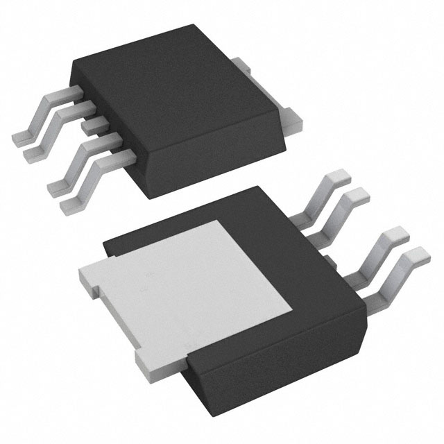
microprocessor reset. The NCV4275C is available in the DPAK and
D2PAK surface mount packages. The output is stable over a wide
output capacitance and ESR range. The NCV4275C is pin for pin
compatible with NCV4275A.
Features
•
•
•
•
•
•
•
5.0 V or 3.3 V ±2% Output Voltage Options
450 mA Output Current
Very Low Current Consumption
Active Reset Output
Reset Low Down to VQ = 1.0 V
500 mV (max) Dropout Voltage
Fault Protection
♦ +45 V Peak Transient Voltage
♦ −42 V Reverse Voltage
♦ Short Circuit Protection
♦ Thermal Overload Protection
AEC−Q100 Qualified and PPAP Capable
These are Pb−Free Devices
•
•
http://onsemi.com
MARKING
DIAGRAMS
1
5
DPAK
5−PIN
DT SUFFIX
CASE 175AA
1
5
4275CxG
ALYWW
1
NC
V4275Cx
AWLYWWG
D2PAK
5−PIN
DS SUFFIX
CASE 936A
x
A
WL, L
Y
WW
G
Applications
• Auto Body Electronics
I
1
= 5 (5.0 V Output)
or 3 (3.3 V Output)
= Assembly Location
= Wafer Lot
= Year
= Work Week
= Pb−Free Package
Q
Error
Amplifier
Bandgap
Reference
ORDERING INFORMATION
Current Limit and
Saturation Sense
See detailed ordering and shipping information on page 13 of
sheet.
+
−
Thermal
Shutdown
Reset
Generator
D
GND
RO
Figure 1. Block Diagram
© Semiconductor Components Industries, LLC, 2014
October, 2019 − Rev. 0
1
Publication Order Number:
NCV4275C/D
�NCV4275C
PIN FUNCTION DESCRIPTION
Pin No.
DPAK−5
D2PAK−5
Symbol
Description
1
I
2
RO
Input; Battery Supply Input Voltage. Bypass to ground with a ceramic capacitor.
3, TAB
GND
4
D
Reset Delay; timing capacitor to GND for Reset Delay function.
5
Q
Output; ±2.0%, 450 mA output. Bypass with 22 mF capacitor, ESR < 4.5 W (5.0 V Version),
3.5 W (3.3 V Version).
Reset Output; Open Collector Active Reset (accurate when I > 1.0 V).
Ground; Pin 3 internally connected to tab.
MAXIMUM RATINGS
Symbol
Min
Max
Unit
Input Voltage
Rating
VI
−42
45
V
Input Peak Transient Voltage
VI
−
45
V
Output Voltage
VQ
−1.0
16
V
Reset Output Voltage
VRO
−0.3
25
V
Reset Output Current
IRO
−5.0
5.0
mA
Reset Delay Voltage
VD
−0.3
7.0
V
Reset Delay Current
ID
−2.0
2.0
mA
ESDHBM
ESDMM
ESDCDM
4.0
200
1000
−
−
−
kV
V
V
Junction Temperature
TJ
−40
150
°C
Storage Temperature
Tstg
−55
150
°C
ESD Susceptibility (Note 1)
− Human Body Model
− Machine Model
− Charge Device Model
Stresses exceeding those listed in the Maximum Ratings table may damage the device. If any of these limits are exceeded, device functionality
should not be assumed, damage may occur and reliability may be affected.
1. This device incorporates ESD protection and is tested by the followign methods: ESD Human Body Model tested per AEC−Q100−002, ESD
Machine Model tested per AEC−Q100−003, ESD Charged Device Model tested per AEC−Q100−011, Latch−up tested per AEC−Q100−004.
OPERATING RANGE
Rating
Input Voltage Operating Range, 5.0 V Output
Symbol
Min
Max
Unit
VI
5.5
42
V
Input Voltage Operating Range, 3.3 V Output
VI
4.4
42
V
Junction Temperature
TJ
−40
150
°C
Functional operation above the stresses listed in the Recommended Operating Ranges is not implied. Extended exposure to stresses beyond the
Recommended Operating Ranges limits may affect device reliability.
LEAD TEMPERATURE SOLDERING REFLOW AND MSL (Note 2)
Rating
Symbol
Min
Max
Unit
Lead Free, 60 sec−150 sec above 217°C
TSLD
−
265 Peak
°C
Moisture Sensitivity Level
MSL
http://onsemi.com
2
1
�NCV4275C
THERMAL CHARACTERISTICS
Characteristic
Test Conditions (Typical Value)
Unit
DPAK 5−PIN PACKAGE
Min Pad Board (Note 3)
1 in Pad Board (Note 4)
Junction−to−Tab (RqJT)
5.1
5.5
°C/W
Junction−to−Ambient (RqJA)
82.4
58.1
°C/W
0.4 sq. in. Spreader Board (Note 5)
1.2 sq. in. Spreader Board (Note 6)
D2PAK
5−PIN PACKAGE
Junction−to−Tab (RqJT)
4.5
4.8
°C/W
Junction−to−Ambient (RqJA)
66.0
49.0
°C/W
2.
3.
4.
5.
6.
PRR IPC / JEDEC J−STD−020C
1 oz. copper, 0.26 inch2 (168 mm2) copper area, 0.062″ thick FR4.
1 oz. copper, 1.14 inch2 (736 mm2) copper area, 0.062″ thick FR4.
1 oz. copper, 0.373 inch2 (241 mm2) copper area, 0.062″ thick FR4.
1 oz. copper, 1.222 inch2 (788 mm2) copper area, 0.062″ thick FR4.
http://onsemi.com
3
�NCV4275C
ELECTRICAL CHARACTERISTICS (VI = 13.5 V; −40°C < TJ < 150°C; unless otherwise noted.)
Characteristic
Symbol
Test Conditions
Min
Typ
Max
4.9
3.23
(2%)
5.0
3.3
5.1
3.37
(2%)
4.9
3.23
(2%)
5.0
3.3
5.1
3.37
(2%)
Unit
Output
Output Voltage
VQ
100 mA v IQ v 400 mA
6.0 V v VI v 28 V (5.0 V Version)
4.4 V v VI v 28 V (3.3 V version)
Output Voltage
VQ
100 mA v IQ v 200 mA
6.0 V v VI v 40 V (5.0 V Version)
4.4 V v VI v 40 V (3.3 V version)
Output Current Limitation
IQ
VQ = 0.9 x VQ,typ
450
650
−
mA
Quiescent Current
Iq = II − IQ
Iq
IQ = 1.0 mA, TJ = 25°C
−
135
150
mA
IQ = 1.0 mA
−
150
200
mA
IQ = 250 mA
−
10
15
mA
IQ = 400 mA
−
23
35
mA
IQ = 300 mA
Vdr = VI − VQ
−
250
500
mV
Dropout Voltage (Note 7)
Vdr
V
V
Load Regulation
DVQ
IQ = 5.0 mA to 400 mA
−30
15
30
mV
Line Regulation
DVQ
DVI = 8.0 V to 32 V,
IQ = 5.0 mA
−15
5.0
15
mV
Power Supply Ripple Rejection
PSRR
fr = 100 Hz, Vr = 0.5 Vpp
−
60
−
dB
Temperature Output Voltage
Drift
dVQ/dT
−−
−
0.5
−
mV/K
Reset Timing D and Output RO
Reset Switching Threshold
5.0 V Version
3.3 V Version
VQ,rt
Vout decreasing
Vin > 5.5 V
Vin > 4.4 V
90
90
93
93
96
96
% Vout
Reset Output Low Voltage
VROL
Rext ≥ 5.0 kW, VQ ≥ 1.0 V
−
0.2
0.4
V
Reset Output Leakage Current
IROH
VROH = 5.0 V
−
0
10
mA
Reset Charging Current
ID,C
VD = 1.0 V
3.0
5.5
9.0
mA
Upper Timing Threshold
VDU
−−
1.5
1.8
2.2
V
Lower Timing Threshold
VDL
−−
0.2
0.4
0.7
V
Reset Delay Time
trd
CD = 47 nF
10
16
22
ms
Reset Reaction Time
trr
CD = 47 nF
−
1.5
4.0
ms
150
−
210
°C
Thermal Shutdown
Shutdown Temperature (Note 8)
TSD
−−
Product parametric performance is indicated in the Electrical Characteristics for the listed test conditions, unless otherwise noted. Product
performance may not be indicated by the Electrical Characteristics if operated under different conditions.
7. Only for 5 V Version. Measured when the output voltage VQ has dropped 100 mV from the nominal value obtained at VI = 13.5 V.
8. Guaranteed by design, not tested in production.
http://onsemi.com
4
�NCV4275C
TYPICAL PERFORMANCE CHARACTERISTICS
5.0 V Version
10
Stable ESR Region
1
Stable ESR Region
1
CQ = 22 mF
ESR (W)
CQ = 22 mF
ESR (W)
3.3 V Version
10
0.1
0.1
VQ(nom) = 5.0 V
0.01
0
100
200
300
VQ(nom) = 3.3 V
0.01
400
0
100
IQ, OUTPUT CURRENT (mA)
200
300
400
IQ, OUTPUT CURRENT (mA)
Figure 2. Output Stability with Output
Capacitor ESR
Figure 3. Output Stability with Output
Capacitor ESR
100
100
10
ESR (W)
ESR (W)
10
Stable ESR Region
1
CQ = 1 mF
Stable ESR Region
1
CQ = 1 mF
0.1
VQ(nom) = 5.0 V
0.01
0
100
VQ(nom) = 3.3 V
200
300
0.1
400
0
100
IQ, OUTPUT CURRENT (mA)
VQ, OUTPUT VOLAGE (V)
5.05
5.03
5.00
4.98
4.95
4.93
3.36
VIN = 13.5 V,
IOUT = 200 mA
3.34
3.32
3.3
3.28
VQ(nom) = 3.3 V
VQ(nom) = 5.0 V
4.90
−40 −20
0
20
40
60
80
400
Figure 5. Output Stability with Output
Capacitor ESR
VQ, OUTPUT VOLAGE (V)
VIN = 13.5 V,
IOUT = 200 mA
5.08
300
IQ, OUTPUT CURRENT (mA)
Figure 4. Output Stability with Output
Capacitor ESR
5.10
200
3.26
−40 −20
100 120 140 160
0
20
40
60
80
100 120 140 160
TJ, JUNCTION TEMPERATURE (°C)
TJ, JUNCTION TEMPERATURE (°C)
Figure 6. Output Voltage VQ vs. Temperature TJ
Figure 7. Output Voltage VQ vs. Temperature TJ
http://onsemi.com
5
�NCV4275C
TYPICAL PERFORMANCE CHARACTERISTICS
5.0 V Version
6
VQ, OUTPUT VOLTAGE (V)
IOUT = 200 mA
TJ = 25°C
5
VQ, OUTPUT VOLTAGE (V)
4.0
4
3
2
1
0
2
4
6
8
IOUT = 200 mA
TJ = 25°C
3.0
2.5
2.0
1.5
1.0
0.5
VQ(nom) = 5.0 V
VQ(nom) = 3.3 V
0.0
0
10
2
8
10
VIN, INPUT VOLTAGE (V)
Figure 9. Output Voltage VQ vs. Input Voltage VIN
VIN = 13.5 V
650
600
550
VQ(nom) = 5.0 V
500
−40 −20
0
20
40
60
80
100 120 140 160
700
VIN = 13.5 V
650
600
550
VQ(nom) = 3.3 V
500
−40 −20
TJ, JUNCTION TEMPERATURE (°C)
0
20
40
60
80
100 120 140 160
TJ, JUNCTION TEMPERATURE (°C)
Figure 10. Output Current IQ vs. Temperature
TJ
Figure 11. Output Current IQ vs. Temperature
TJ
700
700
TJ = 25°C
600
IILIM, ISC, CURRENT LIMIT (mA)
ILIM, ISC, CURRENT LIMIT (mA)
6
VIN, INPUT VOLTAGE (V)
700
TJ = 125°C
500
400
300
200
100
0
4
Figure 8. Output Voltage VQ vs. Input Voltage VIN
IQ, OUTPUT CURRENT LIMITATION (A)
IQ, OUTPUT CURRENT LIMITATION (A)
0
3.5
3.3 V Version
VQ(nom) = 5.0 V
0
5
10
15
20
25
30
35
TJ = 125°C
500
400
300
200
100
0
0
40
TJ = 25°C
600
VIN, INPUT VOLTAGE (V)
VQ(nom) = 3.3 V
5
10
15
20
25
30
35
VI, INPUT VOLTAGE (V)
Figure 12. Output Current IQ vs. Input Voltage
VIN
Figure 13. Output Current IQ vs. Input Voltage
VIN
http://onsemi.com
6
40
�NCV4275C
VIN = 13.5 V,
TJ = 25°C
2.5
2
1.5
1
0.5
VQ(nom) = 5.0 V
0
Iq, CURRENT CONSUMPTION (mA)
Iq, CURRENT CONSUMPTION (mA)
3
0
20
40
60
80
100
120
1.5
1
0.5
VQ(nom) = 3.3 V
0
20
40
60
80
100
Figure 15. Current Consumption Iq vs.
Output Current IQ
120
30
15
10
5
VQ(nom) = 5.0 V
0
50
100
150
200
250
300
350
400
450
VIN = 13.5 V,
TJ = 25°C
25
20
15
10
5
0
VQ(nom) = 3.3 V
IQ, OUTPUT CURRENT (mA)
100 150 200 250 300 350
IQ, OUTPUT CURRENT (mA)
Figure 16. Current Consumption Iq vs.
Output Current IQ
Figure 17. Current Consumption Iq vs.
Output Current IQ
10
0
50
2.2
VIN = 13.5 V,
VD = 1 V
7
6
5
4
3
2
1
0
−40 −20
0
20
40
60
80
450
1.8
1.6
1.4
1.2
1
0.8
0.6
0.4
0.2
0
−40 −20
100 120 140 160
400
VIN = 13.5 V
2
IDC, CHARGE CURRENT (mA)
IDC, CHARGE CURRENT (mA)
2
Figure 14. Current Consumption Iq vs.
Output Current IQ
20
8
2.5
IQ, OUTPUT CURRENT (mA)
VIN = 13.5 V,
TJ = 25°C
25
9
VIN = 13.5 V,
TJ = 25°C
IQ, OUTPUT CURRENT (mA)
30
0
3
0
Iq, CURRENT CONSUMPTION (mA)
Iq, CURRENT CONSUMPTION (mA)
TYPICAL PERFORMANCE CHARACTERISTICS
0
20
40
60
80
100 120 140 160
TJ, JUNCTION TEMPERATURE (°C)
TJ, JUNCTION TEMPERATURE (°C)
Figure 18. Charge Current ID,C vs. Temperature
TJ
Figure 19. Delay Switching Threshold VDU, VDL
vs. Temperature TJ
http://onsemi.com
7
�NCV4275C
TYPICAL PERFORMANCE CHARACTERISTICS
Vdr, DROPOUT VOLTAGE (mV)
800
700
600
500
TJ = 125°C
400
300
TJ = 25°C
200
100
0
VQ(nom) = 5.0 V
0
100
200
300
400
500
600
IQ, OUTPUT CURRENT (mA)
Figure 20. Drop Voltage Vdr vs. Output Current
IQ
http://onsemi.com
8
�NCV4275C
APPLICATION INFORMATION
VI
II
CI1
1000 mF
I
CI2
100 nF
ID
CD
47 nF
1
5
IQ
Q
CQ
22 mF
NCV4275C
D
4
2
3
RO
IRO
VQ
Rext
5.0 k
VRO
GND
Iq
Figure 21. Test Circuit
Circuit Description
The NCV4275C is an integrated low dropout regulator
that provides 5.0 V or 3.3 V, 450 mA protected output and
a signal for power on reset. The regulation is provided by
a PNP pass transistor controlled by an error amplifier with
a bandgap reference, which gives it the lowest possible
drop out voltage and best possible temperature stability.
The output current capability is 450 mA, and the base drive
quiescent current is controlled to prevent over saturation
when the input voltage is low or when the output is
overloaded. The regulator is protected by both current limit
and thermal shutdown. Thermal shutdown occurs above
150°C to protect the IC during overloads and extreme
ambient temperatures. The delay time for the reset output
is adjustable by selection of the timing capacitor. See
Figure 21, Test Circuit, for circuit element nomenclature
illustration.
in Figures 2 to 5. Minimum ESR for CQ = 22 mF is native
ESR of ceramic capacitors. The aluminum electrolytic
capacitor is the least expensive solution, but, if the circuit
operates at low temperatures (−25°C to −40°C), both the
capacitance and ESR of the capacitor will vary considerably.
The capacitor manufacturer’s data sheet usually provides this
information.
The value for the output capacitor CQ shown in
Figure 21, Test Circuit, should work for most applications;
however, it is not necessarily the optimized solution.
Stability is guaranteed for CQ ≥ 22 mF and an ESR ≤ 4.5 W
(5.0 V Version), 3.5 W (3.3 V Version). ESR characteristics
were measured with ceramic capacitors and additional
resistors to emulate ESR. Murata ceramic capacitors were
used, GRM32ER71A226ME20 (22 mF, 10 V, X7R, 1210),
GRM31MR71E105KA01 (1 mF, 25 V, X7R, 1206).
Reset Output
The reset output is used as the power on indicator to the
microcontroller. This signal indicates when the output
voltage is suitable for reliable operation of the controller.
It pulls low when the output is not considered to be ready.
RO is pulled up to VQ by an external resistor, typically
5.0 kW in value. The input and output conditions that
control the Reset Output and the relative timing are
illustrated in Figure 22, Reset Timing.
Output voltage regulation must be maintained for the
delay time before the reset output signals a valid condition.
The delay for the reset output is defined as the amount of
time it takes the timing capacitor on the delay pin to charge
from a residual voltage of 0.0 V to the upper timing
threshold voltage VDU. The charging current for this is ID,C
and D pin voltage in steady state is typically 2.4 V. By using
typical IC parameters with a 47 nF capacitor on the D pin,
the following time delay for 5.0 V regulator is derived:
tRD = CDVDU / ID,C
tRD = 47 nF (1.8 V) / 5.5 mA = 15.4 ms
Regulator
The error amplifier compares the reference voltage to a
sample of the output voltage (VQ) and drives the base of a
PNP series pass transistor by a buffer. The reference is a
bandgap design to give it a temperature−stable output.
Saturation control of the PNP is a function of the load
current and input voltage. Over saturation of the output
power device is prevented, and quiescent current in the
ground pin is minimized.
Regulator Stability Considerations
The input capacitors (CI1 and CI2) are necessary to
stabilize the input impedance to avoid voltage line
influences. Using a resistor of approximately 1.0 W in
series with CI2 can stop potential oscillations caused by
stray inductance and capacitance.
The output capacitor helps determine three main
characteristics of a linear regulator: startup delay, load
transient response and loop stability. The capacitor value
and type should be based on cost, availability, size and
temperature constraints. A tantalum, aluminum or ceramic
capacitors can be used. The range of stability versus
capacitance, load current and capacitive ESR is illustrated
Other time delays can be obtained by changing the
capacitor value.
http://onsemi.com
9
�NCV4275C
VI
t
< Reset Reaction Time
VQ
VQ,rt
t
Reset Charge Current
dVD
+
CD
dt
VD
Upper Timing Threshold VDU
Lower Timing Threshold VDL
t
Reset
Delay Time
Reset
Reaction Time
VRO
t
Power−on−Reset
Thermal
Shutdown
Voltage Dip
at Input
Undervoltage
Secondary
Spike
Figure 22. Reset Timing
http://onsemi.com
10
Overload
at Output
�NCV4275C
Calculating Power Dissipation
in a Single Output Linear Regulator
The maximum power dissipation for a single output
regulator (Figure 23) is:
PD(max) + [VI(max) * VQ(min)] IQ(max)
IQ
II
SMART
REGULATOR®
VI
} Control
Features
(1)
) VI(max)Iq
Iq
where
VI(max)
is the maximum input
voltage,
is the minimum output
VQ(min)
voltage,
IQ(max)
is the maximum output
current for the application,
Iq
is the quiescent current the regulator consumes
at IQ(max).
Once the value of PD(max) is known, the maximum
permissible value of RqJA can be calculated:
T
RqJA + 150° C * A
PD
Figure 23. Single Output Regulator with Key
Performance Parameters Labeled
Heatsinks
A heatsink effectively increases the surface area of the
package to improve the flow of heat away from the IC and
into the surrounding air.
Each material in the heat flow path between the IC and
the outside environment will have a thermal resistance.
Like series electrical resistances, these resistances are
summed to determine the value of RqJA:
RqJA + RqJC ) RqCS ) RqSA
(2)
140
120
100
DPAK 1 oz
60
40
DPAK 2 oz
0
100
200
300
RqJC is the junction−to−case thermal resistance,
RqCS is the case−to−heatsink thermal resistance,
RqSA is the heatsink−to−ambient thermal resistance.
RqJC appears in the package section of the data sheet.
Like RqJA, it too is a function of package type. RqCS and
RqSA are functions of the package type, heatsink and the
interface between them. These values appear in heatsink
data sheets of heatsink manufacturers.
Thermal, mounting, and heatsinking considerations are
discussed in the ON Semiconductor application note
AN1040/D.
RqJA, THERMAL RESISTANCE (C°/W)
RqJA, THERMAL RESISTANCE (C°/W)
160
400
500
600
COPPER AREA SPREADER AREA
700
(3)
where
The value of RqJA can then be compared with those in the
package section of the data sheet. Those packages with
RqJA’s less than the calculated value in Equation 2 will keep
the die temperature below 150°C.
In some cases, none of the packages will be sufficient to
dissipate the heat generated by the IC, and an external
heatsink will be required.
80
VQ
800
140
120
100
80
D2PAK 1 oz
60
40
D2PAK 2 oz
0
(mm2)
100
200
300
400
500
600
COPPER AREA SPREADER AREA
Figure 24. qJA vs. Copper Spreader Area,
DPAK 5−Lead
700
(mm2)
Figure 25. qJA vs. Copper Spreader Area,
D2PAK 5−Lead
http://onsemi.com
11
800
�NCV4275C
100
Cu Area 167 mm2
Cu Area 736 mm2
R(t) C°/W
10
1
0.1
0.000001
0.00001
0.0001
0.001
0.01
0.1
1
10
100
1000
PULSE TIME (sec)
Figure 26. Single−Pulse Heating Curves, DPAK 5−Lead
100
Cu Area 167 mm2
Cu Area 736 mm2
R(t) C°/W
10
1
0.1
0.000001
0.00001
0.0001
0.001
0.01
0.1
1
TIME (sec)
Figure 27. Single−Pulse Heating Curves, D2PAK 5−Lead
http://onsemi.com
12
10
100
1000
�NCV4275C
100
RqJA 736 mm2 C°/W
50% Duty Cycle
10
1.0
20%
10%
5%
2%
1%
0.1
Non−normalized Response
0.01
0.0000001
0.000001
0.00001
0.0001
0.001
0.01
0.1
1.0
10
100
1000
10
100
1000
PULSE WIDTH (sec)
Figure 28. Duty Cycle for 1” Spreader Boards, DPAK 5−Lead
100
RqJA 788 mm2 C°/W
50% Duty Cycle
10
1.0
20%
10%
5%
2%
1%
0.1
Non−normalized Response
0.01
0.0000001
0.000001
0.00001
0.0001
0.001
0.01
0.1
1.0
PULSE WIDTH (sec)
Figure 29. Duty Cycle for 1” Spreader Boards, D2PAK 5−Lead
ORDERING INFORMATION
Device
Output Voltage
NCV4275CDS50R4G
NCV4275CDT50RKG
5.0 V
NCV4275CDS33R4G
NCV4275CDT33RKG
3.3 V
Package
Shipping†
D2PAK
(Pb−Free)
800 / Tape & Reel
DPAK
(Pb−Free)
2500 / Tape & Reel
D2PAK
(Pb−Free)
800 / Tape & Reel
DPAK
(Pb−Free)
2500 / Tape & Reel
†For information on tape and reel specifications,including part orientation and tape sizes, please refer to our Tape and Reel Packaging
Specifications Brochure, BRD8011/D.
http://onsemi.com
13
�MECHANICAL CASE OUTLINE
PACKAGE DIMENSIONS
DPAK−5, CENTER LEAD CROP
CASE 175AA
ISSUE B
DATE 15 MAY 2014
SCALE 1:1
−T−
C
B
V
NOTES:
1. DIMENSIONING AND TOLERANCING
PER ANSI Y14.5M, 1982.
2. CONTROLLING DIMENSION: INCH.
SEATING
PLANE
E
R
R1
Z
A
S
12 3 4 5
U
K
F
J
L
H
D
G
5 PL
0.13 (0.005)
M
T
2.2
0.086
0.34 5.36
0.013 0.217
5.8
0.228
10.6
0.417
0.8
0.031
SCALE 4:1
mm Ǔ
ǒinches
*For additional information on our Pb−Free strategy and soldering
details, please download the ON Semiconductor Soldering and
Mounting Techniques Reference Manual, SOLDERRM/D.
DOCUMENT NUMBER:
DESCRIPTION:
98AON12855D
INCHES
MIN
MAX
0.235 0.245
0.250 0.265
0.086 0.094
0.020 0.028
0.018 0.023
0.024 0.032
0.180 BSC
0.034 0.040
0.018 0.023
0.102 0.114
0.045 BSC
0.170 0.190
0.185 0.210
0.025 0.040
0.020
−−−
0.035 0.050
0.155 0.170
MILLIMETERS
MIN
MAX
5.97
6.22
6.35
6.73
2.19
2.38
0.51
0.71
0.46
0.58
0.61
0.81
4.56 BSC
0.87
1.01
0.46
0.58
2.60
2.89
1.14 BSC
4.32
4.83
4.70
5.33
0.63
1.01
0.51
−−−
0.89
1.27
3.93
4.32
GENERIC
MARKING DIAGRAMS*
RECOMMENDED
SOLDERING FOOTPRINT*
6.4
0.252
DIM
A
B
C
D
E
F
G
H
J
K
L
R
R1
S
U
V
Z
XXXXXXG
ALYWW
AYWW
XXX
XXXXXG
IC
Discrete
XXXXXX
A
L
Y
WW
G
= Device Code
= Assembly Location
= Wafer Lot
= Year
= Work Week
= Pb−Free Package
*This information is generic. Please refer to
device data sheet for actual part marking.
Pb−Free indicator, “G” or microdot “ G”,
may or may not be present.
Electronic versions are uncontrolled except when accessed directly from the Document Repository.
Printed versions are uncontrolled except when stamped “CONTROLLED COPY” in red.
DPAK−5 CENTER LEAD CROP
PAGE 1 OF 1
ON Semiconductor and
are trademarks of Semiconductor Components Industries, LLC dba ON Semiconductor or its subsidiaries in the United States and/or other countries.
ON Semiconductor reserves the right to make changes without further notice to any products herein. ON Semiconductor makes no warranty, representation or guarantee regarding
the suitability of its products for any particular purpose, nor does ON Semiconductor assume any liability arising out of the application or use of any product or circuit, and specifically
disclaims any and all liability, including without limitation special, consequential or incidental damages. ON Semiconductor does not convey any license under its patent rights nor the
rights of others.
© Semiconductor Components Industries, LLC, 2019
www.onsemi.com
�MECHANICAL CASE OUTLINE
PACKAGE DIMENSIONS
D2PAK 5−LEAD
CASE 936A−02
ISSUE E
DATE 28 JUL 2021
SCALE 1:1
GENERIC
MARKING DIAGRAM*
xx
xxxxxxxxx
AWLYWWG
xxxxxx
A
WL
Y
WW
G
= Device Code
= Assembly Location
= Wafer Lot
= Year
= Work Week
= Pb−Free Package
*This information is generic. Please refer to
device data sheet for actual part marking.
Pb−Free indicator, “G” or microdot “G”, may
or may not be present. Some products may
not follow the Generic Marking.
DOCUMENT NUMBER:
DESCRIPTION:
98ASH01006A
D2PAK 5−LEAD
Electronic versions are uncontrolled except when accessed directly from the Document Repository.
Printed versions are uncontrolled except when stamped “CONTROLLED COPY” in red.
PAGE 1 OF 1
ON Semiconductor and
are trademarks of Semiconductor Components Industries, LLC dba ON Semiconductor or its subsidiaries in the United States and/or other countries.
ON Semiconductor reserves the right to make changes without further notice to any products herein. ON Semiconductor makes no warranty, representation or guarantee regarding
the suitability of its products for any particular purpose, nor does ON Semiconductor assume any liability arising out of the application or use of any product or circuit, and specifically
disclaims any and all liability, including without limitation special, consequential or incidental damages. ON Semiconductor does not convey any license under its patent rights nor the
rights of others.
© Semiconductor Components Industries, LLC, 2019
www.onsemi.com
�onsemi,
, and other names, marks, and brands are registered and/or common law trademarks of Semiconductor Components Industries, LLC dba “onsemi” or its affiliates
and/or subsidiaries in the United States and/or other countries. onsemi owns the rights to a number of patents, trademarks, copyrights, trade secrets, and other intellectual property.
A listing of onsemi’s product/patent coverage may be accessed at www.onsemi.com/site/pdf/Patent−Marking.pdf. onsemi reserves the right to make changes at any time to any
products or information herein, without notice. The information herein is provided “as−is” and onsemi makes no warranty, representation or guarantee regarding the accuracy of the
information, product features, availability, functionality, or suitability of its products for any particular purpose, nor does onsemi assume any liability arising out of the application or use
of any product or circuit, and specifically disclaims any and all liability, including without limitation special, consequential or incidental damages. Buyer is responsible for its products
and applications using onsemi products, including compliance with all laws, regulations and safety requirements or standards, regardless of any support or applications information
provided by onsemi. “Typical” parameters which may be provided in onsemi data sheets and/or specifications can and do vary in different applications and actual performance may
vary over time. All operating parameters, including “Typicals” must be validated for each customer application by customer’s technical experts. onsemi does not convey any license
under any of its intellectual property rights nor the rights of others. onsemi products are not designed, intended, or authorized for use as a critical component in life support systems
or any FDA Class 3 medical devices or medical devices with a same or similar classification in a foreign jurisdiction or any devices intended for implantation in the human body. Should
Buyer purchase or use onsemi products for any such unintended or unauthorized application, Buyer shall indemnify and hold onsemi and its officers, employees, subsidiaries, affiliates,
and distributors harmless against all claims, costs, damages, and expenses, and reasonable attorney fees arising out of, directly or indirectly, any claim of personal injury or death
associated with such unintended or unauthorized use, even if such claim alleges that onsemi was negligent regarding the design or manufacture of the part. onsemi is an Equal
Opportunity/Affirmative Action Employer. This literature is subject to all applicable copyright laws and is not for resale in any manner.
PUBLICATION ORDERING INFORMATION
LITERATURE FULFILLMENT:
Email Requests to: orderlit@onsemi.com
onsemi Website: www.onsemi.com
◊
TECHNICAL SUPPORT
North American Technical Support:
Voice Mail: 1 800−282−9855 Toll Free USA/Canada
Phone: 011 421 33 790 2910
Europe, Middle East and Africa Technical Support:
Phone: 00421 33 790 2910
For additional information, please contact your local Sales Representative
�


 工商网监
湘ICP备2023018690号
工商网监
湘ICP备2023018690号
