ON Semiconductor
Is Now
To learn more about onsemi™, please visit our website at
www.onsemi.com
onsemi and and other names, marks, and brands are registered and/or common law trademarks of Semiconductor Components Industries, LLC dba “onsemi” or its affiliates and/or
subsidiaries in the United States and/or other countries. onsemi owns the rights to a number of patents, trademarks, copyrights, trade secrets, and other intellectual property. A listing of onsemi
product/patent coverage may be accessed at www.onsemi.com/site/pdf/Patent-Marking.pdf. onsemi reserves the right to make changes at any time to any products or information herein, without
notice. The information herein is provided “as-is” and onsemi makes no warranty, representation or guarantee regarding the accuracy of the information, product features, availability, functionality,
or suitability of its products for any particular purpose, nor does onsemi assume any liability arising out of the application or use of any product or circuit, and specifically disclaims any and all
liability, including without limitation special, consequential or incidental damages. Buyer is responsible for its products and applications using onsemi products, including compliance with all laws,
regulations and safety requirements or standards, regardless of any support or applications information provided by onsemi. “Typical” parameters which may be provided in onsemi data sheets and/
or specifications can and do vary in different applications and actual performance may vary over time. All operating parameters, including “Typicals” must be validated for each customer application
by customer’s technical experts. onsemi does not convey any license under any of its intellectual property rights nor the rights of others. onsemi products are not designed, intended, or authorized
for use as a critical component in life support systems or any FDA Class 3 medical devices or medical devices with a same or similar classification in a foreign jurisdiction or any devices intended for
implantation in the human body. Should Buyer purchase or use onsemi products for any such unintended or unauthorized application, Buyer shall indemnify and hold onsemi and its officers, employees,
subsidiaries, affiliates, and distributors harmless against all claims, costs, damages, and expenses, and reasonable attorney fees arising out of, directly or indirectly, any claim of personal injury or death
associated with such unintended or unauthorized use, even if such claim alleges that onsemi was negligent regarding the design or manufacture of the part. onsemi is an Equal Opportunity/Affirmative
Action Employer. This literature is subject to all applicable copyright laws and is not for resale in any manner. Other names and brands may be claimed as the property of others.
�NCV7001
Quad Variable Reluctance
Sensor Interface IC
The NCV7001 is a four-channel variable reluctance sensor
interface IC. Microprocessor control functions include two polarity
5.0 V programmable resets, two programmable watchdog inputs, and
an enable function (OLE). Two watchdog inputs allow control from
two independent microprocessors.
Open sensor detection capability is provided. During test mode
(NTEST = Low), a high on the OLE pin should provide a high on the
output. A low under these conditions indicates an open load.
This part has been designed to operate in an automotive
environment.
http://onsemi.com
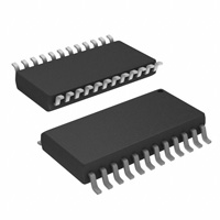
SO-24L
DW SUFFIX
CASE 751E
24
1
Features
•�Four Channel Capability
•�Differential Inputs
•�Open Sensor Detect
•�5.0 V Supply Operation with RESET and Watchdog Features
•�On-Chip Input Voltage Clamping
•�NCV Prefix for Automotive and Other Applications Requiring Site
and Change Control
•�AEC Qualified
•�PPAP Capable
•�Pb-Free Packages are Available*
MARKING DIAGRAM
24
NCV7001
AWLYYWWG
1
A
WL
YY
WW
G
= Assembly Location
= Wafer Lot
= Year
= Work Week
= Pb-Free Package
PIN CONNECTIONS
Typical Applications
•�Antilock Braking Systems (ABS)
•�Traction Control Systems (TCS)
•�Vehicle Dynamics Control (VDC)
RDLY
NTEST
INN1
INP1
INN2
INP2
INP3
INN3
INP4
INN4
THOLD
GND
1
24
NOUT1
NOUT2
WDO
LVI
NLVI
WD2
VCC
WD1
OLE
WDLY
NOUT3
NOUT4
ORDERING INFORMATION
Device
NCV7001DW
NCV7001DWG
NCV7001DWR2
NCV7001DWR2G
*For additional information on our Pb-Free strategy and soldering details, please
download the ON Semiconductor Soldering and Mounting Techniques
Reference Manual, SOLDERRM/D.
©� Semiconductor Components Industries, LLC, 2007
October, 2007 - Rev. 4
1
Package
Shipping†
SO-24L
30 Units/Rail
SO-24L
(Pb-Free)
30 Units/Rail
SO-24L
1000 Tape & Reel
SO-24L
(Pb-Free)
1000 Tape & Reel
†For information on tape and reel specifications,
including part orientation and tape sizes, please
refer to our Tape and Reel Packaging Specification
Brochure, BRD8011/D.
Publication Order Number:
NCV7001/D
�NCV7001
22 k
Variable
Reluctance
Sensor
1/4 W
0.001 mF
200 V
22 k
0.01 mF
50 V
0.047 mF
0.01 mF
50 V
1/4 W
22 k
Variable
Reluctance
Sensor
1/4 W
0.001 mF
200 V
22 k
0.01 mF
50 V
0.01 mF
50 V
47 k
RDLY
NOUT1
NTEST
NOUT2
INN1
WDO
INP1
LVI
INN2
NLVI
INP2
WD2
INP3
VCC
INN3
WD1
INP4
OLE
INN4
WDLY
47 k
1/4 W
22 k
Variable
Reluctance
Sensor
1/4 W
0.001 mF
200 V
22 k
0.01 mF
50 V
0.01 mF
50 V
1/4 W
THOLD
NOUT3
GND
NOUT4
22 k
Variable
Reluctance
Sensor
1/4 W
0.001 mF
200 V
22 k
NCV7001
0.1 mF
VCC
0.1 mF
47 k
0.01 mF
50 V
0.01 mF
50 V
1/4 W
Figure 1. Application Diagram
MAXIMUM RATINGS*
Rating
Value
Unit
-0.3 to 7.0
V
-10, 10
mA
2.0
kV
Storage Temperature
-55 to 150
°C
Operating Junction Temperature
-40 to 150
°C
16
80
°C/W
°C/W
240 peak
°C
DC Supply Voltage (VCC)
Input Clamp Current
ESD Capability (Human Body Model)
Package Thermal Resistance:
Junction-to-Case, RqJC
Junction-to-Ambient, RqJA
Lead Temperature Soldering:
Reflow: (SMD styles only) (Notes 1, 2)
Stresses exceeding Maximum Ratings may damage the device. Maximum Ratings are stress ratings only. Functional operation above the
Recommended Operating Conditions is not implied. Extended exposure to stresses above the Recommended Operating Conditions may affect
device reliability.
*The maximum package power dissipation must be observed.
1. 60 second maximum above 183°C.
2. -5°C/+0°C allowable conditions.
http://onsemi.com
2
�NCV7001
ELECTRICAL CHARACTERISTICS (4.5 V ≤ VCC ≤ 5.5 V, -40°C ≤ TJ ≤ 125°C; unless otherwise noted.)
Characteristic
Test Conditions
Min
Typ
Max
Unit
-
-
-
24
mA
General Characteristics
Quiescent Current
Input
Positive Input Threshold
Rseries = 22 k between INPX & INNX
Thold Pin = 0 V
30
45
60
mV
Negative Input Threshold
Rseries = 22 k between INPX & INNX
Thold Pin = 0 V
-60
-45
-30
mV
Positive Input Threshold
Rseries = 22 k between INPX & INNX
Thold Pin = 2.0 V
84
126
168
mV
Negative Input Threshold
Rseries = 22 k between INPX & INNX
Thold Pin = 2.0 V
-168
-126
-84
mV
Positive Input Threshold
Rseries = 22 k between INPX & INNX
±90 mV at VCC = VTHOLD = 4.5 V
110
140
200
mV
Negative Input Threshold
Rseries = 22 k between INPX & INNX
±90 mV at VCC = VTHOLD = 4.5 V
-200
-140
-110
mV
Input Resistance
-
225
400
800
kW
0.46 VCC
0.5 VCC
0.54 VCC
V
-6.0
-
6.0
mA
-0.5
VCC - 0.6
0
VCC
0.5
VCC + 0.6
V
V
22 k in Series with INNX and INPX
12
-
120
kW
Output Low Voltage
IOUT = 1.0 mA
-
0.2
0.4
V
Output High Voltage
IOUT = -100 mA
VCC - 0.7
-
-
V
Output During Test /
Normal Sensor (VCC - VOUT)
OLE = 1.0, IOUT = -100 mA
-
-
0.7
V
Output During Test /
Open Sensor (VCC - VOUT)
OLE = 1.0, IOUT = -1.0 mA
-
-
0.4
V
Output (VCC - VOUT)
OLE (= Low), IOUT = -100 mA,
-
-
0.7
V
Output (VCC - VOUT)
OLE ( = 1.0)/Normal Sensor, NO Signal
from Sensor, IOUT = -100 mA
-
-
0.4
V
Watchdog Output Low Voltage
IWDO = 1.0 mA
-
0.2
0.4
V
Watchdog Output High Leakage
VWDO = VCC
Input Bias/Single Ended
Thold = 0 V
Input Clamp Current
For Correct Reset & Watchdog During
Power Up
Input Clamp Voltage
(-10 mA)
(+10 mA)
Open Sensor Threshold
Output (NOUTX)
Logic
Watchdog Input Voltage High
Watchdog Input Voltage Low
-
-
-
10
mA
-
1.5
2.0
V
-
0.8
1.4
-
V
Watchdog Input Pullup Current
WD1 = WD2 = 2.0 V
-30
-
-450
mA
Watchdog Input Pullup Current
WD1 = WD2 = 0.8 V
-50
-
-600
mA
Thold Pin Input Current
0.3 V < VTHOLD < VCC
-
5.0
40
mA
Test Input Low Threshold
-
0.3 VCC
-
-
V
Test Input High Threshold
-
-
-
0.7 VCC
V
-25
-
220
mA
OLE Input Low Threshold
-
0.8
1.4
-
V
OLE Input High Threshold
-
-
1.5
2.0
V
Test Input Current
VIN = 0.7 VCC, TEST = 1
OLE Input Current
OLE = 1.0, VIN = 2.0 V
-30
-
-450
mA
OLE Input Current
OLE = Low, VIN = 0.8 V
-50
-
-600
mA
http://onsemi.com
3
�NCV7001
ELECTRICAL CHARACTERISTICS (continued) (4.5 V ≤ VCC ≤ 5.5 V, -40°C ≤ TJ ≤ 125°C; unless otherwise noted.)
Characteristic
Test Conditions
Min
Typ
Max
Unit
Low Voltage Reset
Timeout Delay
VCC - Increasing 0 to 5.0 V
30
50
70
ms
Reset Delay
VCC - Decreasing 5.0 to 4.25 V
-
-
1.0
ms
NLVI Rise and Fall Time
10 k Pullup & CL = 30 pF
-
-
50
ms
LVI Rise and Fall Time
57 k Pulldown & CL = 30 pF
-
-
50
ms
Threshold High VCC Going Up
-
-
4.66
4.75
V
Threshold Low VCC Going Low
-
4.5
4.59
-
V
Threshold Hysteresis
LVTH - LVTL
30
70
-
mV
NLVI Output Low
25°C ≤ T ≤ 125°C, VCC = 1.0 V,
INLVI = 1.0 mA
-40°C ≤ T ≤ 125°C, VCC = 1.2 V,
INLVI = 1.0 mA
-
150
300
mV
-
150
300
mV
NLVI Output Low
VCC = 4.5 V @ -40°C, INLVI = 2.5 mA
-
150
300
mV
NLVI Output Leakage
VNLI = VCC
-10
-
10
mA
LVI Output High
VCC = 1.0 V, ILV = -36 mA
0.8
0.9
-
V
LVI Output High
VCC = 4.5 V, ILV = -250 mA
3.6
4.3
-
V
LVI Output Leakage
4.75 < VCC 5.25 V, VLVC = 0 V
-7.5
-
7.5
mA
Watchdog Short Time Detect
(Watchdog Running at 300 Hz)
4.56
6.075
7.59
ms
Watchdog Long Time Detect
(Watchdog Running at 33 Hz)
13.7
18.25
22.8
ms
Watchdog Skew Time Detect
(Difference between WD1 & WD2)
0.7
-
2.1
ms
Timing Specs
Watchdog Timeout Delay Time
-
Output Rise Time
CL = 30 pF
Output Fall Time
CL = 30 pF
30
50
70
ms
-
0.5
2.0
ms
-
0.05
2.0
ms
Delay Input to Output
-
-
1.0
20
ms
OLE Delay to NOUT
-
-
1.0
20
ms
http://onsemi.com
4
�NCV7001
PIN DESCRIPTION
ÁÁÁÁÁ
ÁÁÁÁÁÁÁÁÁÁÁÁÁÁÁÁÁÁÁÁÁÁÁÁÁ
ÁÁÁÁÁÁÁÁÁÁ
ÁÁÁÁÁ
ÁÁÁÁÁÁÁÁÁÁÁÁÁÁÁÁÁÁÁÁÁÁÁÁÁ
ÁÁÁÁÁ
ÁÁÁÁÁ
ÁÁÁÁÁÁÁÁÁÁÁÁÁÁÁÁÁÁÁÁÁÁÁÁÁ
ÁÁÁÁÁ
ÁÁÁÁÁ
ÁÁÁÁÁÁÁÁÁÁÁÁÁÁÁÁÁÁÁÁÁÁÁÁÁ
ÁÁÁÁÁ
ÁÁÁÁÁ
ÁÁÁÁÁÁÁÁÁÁÁÁÁÁÁÁÁÁÁÁÁÁÁÁÁ
ÁÁÁÁÁ
ÁÁÁÁÁ
ÁÁÁÁÁÁÁÁÁÁÁÁÁÁÁÁÁÁÁÁÁÁÁÁÁ
ÁÁÁÁÁÁÁÁÁÁ
ÁÁÁÁÁÁÁÁÁÁÁÁÁÁÁÁÁÁÁÁÁÁÁÁÁ
ÁÁÁÁÁÁÁÁÁÁ
ÁÁÁÁÁÁÁÁÁÁÁÁÁÁÁÁÁÁÁÁÁÁÁÁÁ
ÁÁÁÁÁ
ÁÁÁÁÁ
ÁÁÁÁÁÁÁÁÁÁÁÁÁÁÁÁÁÁÁÁÁÁÁÁÁ
ÁÁÁÁÁ
ÁÁÁÁÁ
ÁÁÁÁÁÁÁÁÁÁÁÁÁÁÁÁÁÁÁÁÁÁÁÁÁ
ÁÁÁÁÁ
ÁÁÁÁÁ
ÁÁÁÁÁÁÁÁÁÁÁÁÁÁÁÁÁÁÁÁÁÁÁÁÁ
ÁÁÁÁÁ
ÁÁÁÁÁ
ÁÁÁÁÁÁÁÁÁÁÁÁÁÁÁÁÁÁÁÁÁÁÁÁÁ
ÁÁÁÁÁ
ÁÁÁÁÁÁÁÁÁÁÁÁÁÁÁÁÁÁÁÁÁÁÁÁÁ
ÁÁÁÁÁÁÁÁÁÁ
ÁÁÁÁÁ
ÁÁÁÁÁÁÁÁÁÁÁÁÁÁÁÁÁÁÁÁÁÁÁÁÁ
ÁÁÁÁÁ
ÁÁÁÁÁ
ÁÁÁÁÁÁÁÁÁÁÁÁÁÁÁÁÁÁÁÁÁÁÁÁÁ
ÁÁÁÁÁ
ÁÁÁÁÁ
ÁÁÁÁÁÁÁÁÁÁÁÁÁÁÁÁÁÁÁÁÁÁÁÁÁ
ÁÁÁÁÁ
ÁÁÁÁÁ
ÁÁÁÁÁÁÁÁÁÁÁÁÁÁÁÁÁÁÁÁÁÁÁÁÁ
ÁÁÁÁÁ
ÁÁÁÁÁ
ÁÁÁÁÁÁÁÁÁÁÁÁÁÁÁÁÁÁÁÁÁÁÁÁÁ
ÁÁÁÁÁ
ÁÁÁÁÁ
ÁÁÁÁÁÁÁÁÁÁÁÁÁÁÁÁÁÁÁÁÁÁÁÁÁ
ÁÁÁÁÁ
ÁÁÁÁÁÁÁÁÁÁÁÁÁÁÁÁÁÁÁÁÁÁÁÁÁ
ÁÁÁÁÁÁÁÁÁÁ
ÁÁÁÁÁ
ÁÁÁÁÁÁÁÁÁÁÁÁÁÁÁÁÁÁÁÁÁÁÁÁÁ
ÁÁÁÁÁ
ÁÁÁÁÁ
ÁÁÁÁÁÁÁÁÁÁÁÁÁÁÁÁÁÁÁÁÁÁÁÁÁ
ÁÁÁÁÁ
ÁÁÁÁÁ
ÁÁÁÁÁÁÁÁÁÁÁÁÁÁÁÁÁÁÁÁÁÁÁÁÁ
ÁÁÁÁÁ
ÁÁÁÁÁ
ÁÁÁÁÁÁÁÁÁÁÁÁÁÁÁÁÁÁÁÁÁÁÁÁÁ
ÁÁÁÁÁÁÁÁÁÁ
ÁÁÁÁÁÁÁÁÁÁÁÁÁÁÁÁÁÁÁÁÁÁÁÁÁ
Pin No.
Symbol
Description
1
RDLY
2
NTEST
Low = test, high = normal operation.
3
INN1
Minus input to channel 1 comparator.
4
INP1
Plus input to channel 1 comparator.
5
INN2
Minus input to channel 2 comparator.
6
INP2
Plus input to channel 2 comparator.
7
INP3
Plus input to channel 3 comparator.
8
INN3
Minus input to channel 3 comparator.
9
INP4
Plus input to channel 4 comparator.
10
INN4
Minus input to channel 4 comparator.
11
THOLD
12
GND
13
NOUT4
Inverted output of comparator 4.
14
NOUT3
Inverted output of comparator 3.
15
WDLY
Determines watchdog timing.
Determines the low voltage reset delay and watchdog enable and disable delay.
Variable threshold adjustment.
Ground.
16
OLE
Disables outputs. High = normal operation. Low = forces all outputs and comparators high.
17
WD1
Watchdog input.
18
VCC
5.0 V input to IC.
19
WD2
Watchdog input.
20
NLVI
Reset output (in reset when low).
21
LVI
Reset output (in reset when high).
22
WDO
23
NOUT2
Watchdog output (low for valid watchdog signal).
Inverted output of comparator 2.
24
NOUT1
Inverted output of comparator 1.
Table 1. Wheel Speed Output Functionality
Sensor
NTEST
OLE
NOUTx
OPEN
L
L
H
OPEN
L
H
L
OPEN
H
L
H
OPEN
H
H
X
NORMAL
L
L
H
NORMAL
L
H
H
NORMAL
H
L
H
NORMAL
H
H
X
†X = Do not care (dependent on presence of sensor signal).
http://onsemi.com
5
�NCV7001
VCC
LVI
Bandgap
Regulator
INN1
0.5 VCC
RESET
NLV
VBG
+
-
RDL
NOUT1
INP1
VBG
VCC
+
-
+
-
THOLD
VCC
INN2
0.5 VCC
+
NOUT2
INP2
VBG
VCC
+
VCC
INN3
0.5 VCC
+
NOUT3
INP3
VBG
VCC
VCC
+
-
WD1
WD2
VCC
Watchdog
WDO
INN4
0.5 VCC
+
-
WDLY
NOUT4
INP4
VBG
VCC
VCC
NTEST
+
-
VCC
OLE
GND
Figure 2. Block Diagram
http://onsemi.com
6
�NCV7001
PACKAGE DIMENSIONS
SO-24L
DW SUFFIX
CASE 751E-04
ISSUE E
-A24
NOTES:
1. DIMENSIONING AND TOLERANCING PER ANSI
Y14.5M, 1982.
2. CONTROLLING DIMENSION: MILLIMETER.
3. DIMENSIONS A AND B DO NOT INCLUDE
MOLD PROTRUSION.
4. MAXIMUM MOLD PROTRUSION 0.15 (0.006)
PER SIDE.
5. DIMENSION D DOES NOT INCLUDE DAMBAR
PROTRUSION. ALLOWABLE DAMBAR
PROTRUSION SHALL BE 0.13 (0.005) TOTAL IN
EXCESS OF D DIMENSION AT MAXIMUM
MATERIAL CONDITION.
13
-B-
12X
P
0.010 (0.25)
1
M
B
M
12
24X
D
J
0.010 (0.25)
M
T A
S
B
S
F
R
X 45 _
C
-TSEATING
PLANE
M
22X
G
K
DIM
A
B
C
D
F
G
J
K
M
P
R
MILLIMETERS
MIN
MAX
15.25
15.54
7.40
7.60
2.35
2.65
0.35
0.49
0.41
0.90
1.27 BSC
0.23
0.32
0.13
0.29
0_
8_
10.05
10.55
0.25
0.75
INCHES
MIN
MAX
0.601
0.612
0.292
0.299
0.093
0.104
0.014
0.019
0.016
0.035
0.050 BSC
0.009
0.013
0.005
0.011
0_
8_
0.395
0.415
0.010
0.029
ON Semiconductor and
are registered trademarks of Semiconductor Components Industries, LLC (SCILLC). SCILLC reserves the right to make changes without further notice
to any products herein. SCILLC makes no warranty, representation or guarantee regarding the suitability of its products for any particular purpose, nor does SCILLC assume any liability
arising out of the application or use of any product or circuit, and specifically disclaims any and all liability, including without limitation special, consequential or incidental damages.
“Typical” parameters which may be provided in SCILLC data sheets and/or specifications can and do vary in different applications and actual performance may vary over time. All
operating parameters, including “Typicals” must be validated for each customer application by customer's technical experts. SCILLC does not convey any license under its patent rights
nor the rights of others. SCILLC products are not designed, intended, or authorized for use as components in systems intended for surgical implant into the body, or other applications
intended to support or sustain life, or for any other application in which the failure of the SCILLC product could create a situation where personal injury or death may occur. Should
Buyer purchase or use SCILLC products for any such unintended or unauthorized application, Buyer shall indemnify and hold SCILLC and its officers, employees, subsidiaries, affiliates,
and distributors harmless against all claims, costs, damages, and expenses, and reasonable attorney fees arising out of, directly or indirectly, any claim of personal injury or death
associated with such unintended or unauthorized use, even if such claim alleges that SCILLC was negligent regarding the design or manufacture of the part. SCILLC is an Equal
Opportunity/Affirmative Action Employer. This literature is subject to all applicable copyright laws and is not for resale in any manner.
PUBLICATION ORDERING INFORMATION
LITERATURE FULFILLMENT:
Literature Distribution Center for ON Semiconductor
P.O. Box 5163, Denver, Colorado 80217 USA
Phone: 303-675-2175 or 800-344-3860 Toll Free USA/Canada
Fax: 303-675-2176 or 800-344-3867 Toll Free USA/Canada
Email: orderlit@onsemi.com
N. American Technical Support: 800-282-9855 Toll Free
USA/Canada
Europe, Middle East and Africa Technical Support:
Phone: 421 33 790 2910
Japan Customer Focus Center
Phone: 81-3-5773-3850
http://onsemi.com
7
ON Semiconductor Website: www.onsemi.com
Order Literature: http://www.onsemi.com/orderlit
For additional information, please contact your local
Sales Representative
NCV7001/D
�