NCV7471B5V1GEVB,
NCV7471C5V1GEVB,
NCV7471C5V2GEVB
NCV7471 System Basis
Chip Evaluation Board
User's�Manual
www.onsemi.com
EVAL BOARD USER’S MANUAL
Introduction
Evaluation Board Features
• One−row Pin Header, Providing the Circuit Signals,
This document describes the NCV7471 EVB board for the
ON Semiconductor NCV7471 System basis chip with a
high−speed CAN and two LIN transceivers with boost−buck
converter and low−drop voltage regulator. The functionality
and major parameters can be evaluated with the NCV7471
EVB board.
NCV7471 is a System Basis Chip (SBC) integrating
functions typically found in automotive Electronic Control
Units (ECUs) in the body domain. NCV7471 provides and
monitors the low−voltage power supplies for the application
microcontroller and other loads, monitors the application
software via a watchdog and includes high−speed CAN and
LIN transceivers allowing the ECU to host multiple
communication nodes or to act as a gateway unit. The
on−chip state controller ensures safe power−up sequence
and supports low−power modes with a configurable set of
features including wakeup from the communication buses
or by a local digital signal WU. The status of several
NCV7471 internal blocks can be read by the microcontroller
through the serial peripheral interface or can be used to
generate an interrupt request.
•
•
•
•
•
•
•
•
•
•
Enables Easy Insertion of the Evaluation Board into a
more Complex Application Setup
Oscilloscope Test−points on All Important Signals
Reverse Protection and Decoupling on the Main
(Battery) Supply
All the Necessary VOUT Converter External
Components – Assembly Options Available
Decoupling on VOUT Converter and VOUT2
Regulator Outputs
Additional Pull−up Resistors on the Open−drain Digital
Outputs (RSTN, INTN, UVN_VOUT)
Filtering Circuit on the Switch−monitoring WAKE
Input
On−board Local Wakeup Switch
CAN/LIN−bus Terminations
Good Thermal Connection of the Circuit’s Exposed Pad
to the Bottom Ground Plane
Basic Standalone Functionality using Software
Development Mode
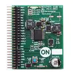
Figure 1. Evaluation Board Photo
© Semiconductor Components Industries, LLC, 2014
July, 2018 − Rev. 2
1
Publication Order Number:
EVBUM2219/D
�NCV7471B5V1GEVB, NCV7471C5V1GEVB, NCV7471C5V2GEVB
SCHEMATIC
Complete schematic with all the assembly options are
shown in Figure 2. Depending on VOUT maximum current
and minimum battery operation voltage, few assembly
options are available. Values of components may be
customized according to specific requirements.
Figure 2. NCV7471 Evaluation Board Schematic
www.onsemi.com
2
�NCV7471B5V1GEVB, NCV7471C5V1GEVB, NCV7471C5V2GEVB
Table 1. ABSOLUTE MAXIMUM RATINGS
Rating
Pins
Min
Max
Unit
Vbat
−40
40
V
VOUT output voltage
VOUT
−0.3
6
V
VOUT output current
VOUT
0
internally limited
mA
VOUT2 output voltage
VOUT2
−1
40
V
VOUT2 output current
VOUT2
0
internally limited
mA
Digital inputs voltage
RSTN, INTN, UVN, SDI, SCK, CSN,
TxDC, TxDL1/2
−0.3
6
V
SDO, RxDC, RxDL1/2
−0.3
VOUT+0.3
V
Supply voltage
Digital outputs voltage
Fail−safe pin output voltage
FSO
−0.3
40
V
LIN bus lines voltage
LIN1, LIN2
−45
45
V
CAN bus lines voltage
CANH, CANL
−50
50
V
Wake−up input voltage
WU
−40
40
V
NCV7471 junction temperature
−40
+170
°C
Board temperature
−40
+125
°C
Stresses exceeding those listed in the Maximum Ratings table may damage the device. If any of these limits are exceeded, device functionality
should not be assumed, damage may occur and reliability may be affected.
Table 2. RECOMMENDED BOARD OPERATING CONDITIONS
Rating
Pins
Min
Vbat
NCV7471B5V1GEVB
NCV7471C5V1GEVB
NCV7471C5V2GEVB
6.6
3.8
3.0
Supply voltage (VS)
VS (board internal node)
NCV7471B5V1GEVB
NCV7471C5V1GEVB
NCV7471C5V2GEVB
6.0
3.3
2.5
VOUT output voltage
VOUT
4.9
VOUT output current
VOUT
NCV7471B5V1GEVB
NCV7471C5V1GEVB
NCV7471C5V2GEVB
0
VOUT2
4.9
VOUT2 output current
VOUT2
Digital inputs voltage
RSTN, INTN, UVN, SDI, SCK, CSN,
TxDC, TxDL1/2
Digital outputs voltage
FSO pin output voltage
Supply voltage (Vbat)
VOUT2 output voltage
Max
Unit
28
V
28
V
5.1
V
250
250
500
mA
5.1
V
0
50
mA
0
VOUT
V
SDO, RxDC, RxDL1/2
0
VOUT
V
FSO
0
VS
V
LIN bus lines voltage
LIN1, LIN2
0
VBAT
V
CAN bus lines voltage
CANH, CANL
0
5
V
Wake−up input voltage
WU
0
VBAT
V
NCV7471 junction temperature
−40
+150
°C
Board temperature
−40
+105
°C
Functional operation above the stresses listed in the Recommended Operating Ranges is not implied. Extended exposure to stresses beyond
the Recommended Operating Ranges limits may affect device reliability.
*See assembly options
www.onsemi.com
3
�NCV7471B5V1GEVB, NCV7471C5V1GEVB, NCV7471C5V2GEVB
OPERATIONAL GUIDELINES
• CAN transceiver is configured into LIN Normal mode
NCV7471 is complex SCB device, which needs external
MCU, connected through H1 connector, to control all
functions and settings. However, with basic function of the
converter, LIN and CAN operation, NCV7471 may work in
so called Software Development Mode (SWDM). To
configure NCV7471 into this mode, SWDM pin has to be
tight to VS. Details about board configuration can be found
in the following chapter.
Behavior of NCV7174 in Software Development mode is
following:
• Buck converter is active, delivering +5 V on VOUT.
• Boost converter may be disabled/enabled by connecting
CFG pin to GND/VS (“−”/“+” positions of CFG
soldering strap)
• VOUT2 LDO is disabled by default
– receiver and transmitter are enabled.
• LIN1/2 transceiver is configured into LIN Normal
•
•
mode – receiver and transmitter are enabled.
Watchdog does not need to be served, the device
remains in Normal mode, until it is changed via SPI
command.
RSTN, INTN, VOUT_UVN, FSO1−3 provide their
standard functionality, except of RSTN and FSO1−3
pins, which are not active due to not−serving the
watchdog.
Board Configuration
The NCV7471 evaluation board provides few hardware
configuration options, using soldering straps. Their
functions are described in the table below.
Table 3. SOLDERING STRAPS FUNCTIONS
Solder Strap
Position
SWDM
“−” or not connected
(GND)
“+”
(VS)
CFG
“−” or not connected
(GND)
“+”
(VS)
VS_VOUT2
FSO1−3
VS
Function
Normal operation mode with external MCU connected (Watchdog service needed)
Software Development Mode (Watchdog does not need to be served, CAN and LIN1/2
enabled in Normal mode by default)
SWDM = GND: Config2/4 (Fail−safe mode entered after 1st/2nd watchdog service failure)
SWDM = VS: Boost stage disabled
SWDM = GND: Config1/3 (Fail−safe mode not entered after 1st/2nd watchdog service
failure)
SWDM = VS: Boost stage enabled
Input of VOUT2 LDO regulator connected to VS
VMID
Input of VOUT2 LDO regulator connected to V_MID
FSO1
FSO constantly Low at failure
FSO2
FSO Low for 50%, frequency of 1.25 Hz at failure
FSO3
FSO Low for 20%, frequency of 100 Hz at failure
Special care has to be taken for Standby or Sleep mode
quiescent consumption measurements. Both SWDM and
CFG pins have internal pull−down resistors (typ. 100 kW),
which influence input supply current if they are connected
to VS (typically Software Development Mode with Boost
stage enabled). To measure pure NCV7471 consumption,
these pins should stay Low (GND) or may be pulled up by
external voltage source.
Four on−board LEDs indicate faulty states of the board, as
described in the Table 4.
www.onsemi.com
4
�NCV7471B5V1GEVB, NCV7471C5V1GEVB, NCV7471C5V2GEVB
Table 4. LED FUNCTIONS
LED Name
Function
LED_RSTN
Indicates activation of RSTN pin due to the following reasons:
• Sleep/Fail−safe mode (LED_RSTN off due to missing VOUT supply),
• Reset mode (internal or external activation) (5 ms on)
LED_INTN
Indicates activation of INTN pin due to the following reasons:
• Sleep/Fail−safe mode (LED_INTN off due to missing VOUT supply),
• Wake−up event (CAN, LIN1/2, WU, Timer) – configurable via SPI
• Interrupt request – has to be enabled via SPI (1 ms on, 5 ms off)
LED_UVN
Indicates activation of VOUT_UVN pin due to the following reasons:
• Sleep/Fail−safe mode (LED_UVN off due to missing VOUT supply),
• Undervoltage on VOUT pin (VOUT < 4.65 V)
LED_FSO
FSOx pin active due to failure condition (depends on CFG and SPI configuration):
• Thermal Shutdown
• Fatal VOUT failure
• RSTN clamped Low / High
• Watchdog failure (ignored if SWDM is High)
• SPI control bit FSO_ON is set
External Board Connections
For basic evaluation, the board may operate without
external control in the Software Development Mode
(Figure 3). If full functionality is needed, an external
microcontroller has to be attached to the board (Figure 4).
Configuration with and without the control MCU is
shown in the figures below. SWDM and CFG soldering
straps need to be configured to work correctly in both setups.
VCC
MCU
CAN
SPI
CAN
LIN1
LIN1
LIN2
GND
LIN2
FSO electronic
sensor
GND
VBAT
GND
VBAT
CANL
CANH
CANL
CANH
LIN1
LIN1
LIN2
LIN2
Figure 3. Standalone NCV7471 Evaluation Setup
(Software Development Mode used, limited
functionality)
Figure 4. NCV 7471 Full Evaluation Setup
www.onsemi.com
5
�NCV7471B5V1GEVB, NCV7471C5V1GEVB, NCV7471C5V2GEVB
FUNCTIONAL DESCRIPTION
VS Supply Input
modulation frequency of 10 kHz and three SPI−selectable
modulation depth values – 10%, 20% or 30% of the nominal
frequency.
VOUT level is monitored by an under−voltage detector
with multiple thresholds:
• Comparison with selectable threshold VOUT_RESx. By
default, the lowest threshold (typ. 3.1 V) applies for the
state machine control and the activation of the RSTN
signal (LED_RSTN on). This reset threshold can be
changed via SPI to any of the four programmable
values.
• A second monitoring signal – UVN_VOUT
(LED_UVN on) – is generated based on comparison of
the VOUT level with the highest monitoring level (typ.
4.65 V).
• VOUT is compared with a fixed threshold VOUT_FAIL
(typ. 2 V). If VOUT stays below VOUT_FAIL level for
longer than t_VOUT_powerup (typ. 1.5 s), a VOUT
short−circuit is detected and Fail−safe mode is entered
(LED_FSO on, if connected).
VS pin of NCV7471 is typically connected to the car
battery through a reverse−protection diode and can be
exposed to all relevant automotive disturbances (ISO7637
pulses, system ESD ...). VS supplies mainly the integrated
LIN transceivers.
VOUT DC/DC Converter
The main application low−voltage supply is provided by
an integrated boost−buck DC/DC converter, delivering a
5 V output VOUT. The converter can work in two modes:
• Buck−only mode is the default mode of the VOUT
power−supply. In this mode, the boosting part of the
converter is never activated and the resulting VOUT
voltage can be only lower than the input line voltage.
Buck−only mode is applied during the initial power−up
(after the VS connection), wakeup from Sleep−mode
and also recovery from the Fail−safe mode, as well as
in the Software Development Mode with CFG pin at
Low level.
• Boost−buck mode ensures that the correct VOUT
voltage is generated even if the input line voltage falls
below the required VOUT level. This mode can be
requested through the corresponding SPI control
register. If selected, the boost−buck mode is used
during Reset, Start−up, Normal, Standby, and Flash
modes. It is also preserved during VOUT
under−voltage recovery through Power−up mode. In
SW Development configuration, boost−buck mode can
be additionally enabled by High level on CFG pin. No
SPI communication is therefore necessary to select the
DC/DC mode in SW Development (see Table 5).
Both UVN_VOUT and RSTN pins provide an open drain
output with integrated pull−up resistor. The split between
reset−generating level VOUT_RESx and an under−voltage
indication allows coping with VOUT dips in case of high
loads coinciding with low input line voltages.
VOUT2 Low−drop Regulator
An integrated low−drop regulator provides a second 5 V
supply VOUT2 to external loads, typically sensors. The
regulator’s input is taken from a dedicated pin VS_VOUT2,
which does not feature an explicit under−voltage
monitoring. VS_VOUT2 would be typically connected to
the VS pin or might be taken from other nodes like, e.g., the
DC/DC converter’s auxiliary node V_MID. “VS_VOUT2”
soldering strap allows connecting VOUT2 LDO input
supply to the VS or the V_MID point.
After a power−up or a reset event, as well as in Sleep
mode, VOUT2 regulator is switched off. In Start−up,
Normal, Standby and Flash modes, it can be freely activated
or deactivated via SPI control register.
Table 5. CONTROL OF DC/DC CONVERTER MODES
(“X” means “Don’t care”)
Device
Configuration
SPI bit enBOOST
CFG Pin
Signal
Applied DC/DC
Mode
Config 1, 2, 3, 4
Low
X
Buck−Only
High
SW Development
Low
High
Boost−Buck
Low
Buck−Only
High
Boost−Buck
X
Boost−Buck
Operating States
NCV7471 provides five static operating modes and three
transition states – see Figure 5. Mode setting is done via SPI
registers. Additional details of the NCV7471 operation and
parameters can be found in the corresponding NCV7471/D
datasheet at www.onsemi.com.
By default, the converter works with a fixed switching
frequency 485 kHz nominal. Through the SPI settings, a
switching frequency modulation can be applied with fixed
www.onsemi.com
6
�NCV7471B5V1GEVB, NCV7471C5V1GEVB, NCV7471C5V2GEVB
FAIL−SAFE
Failure
Event
Any
mode
SPI
Any Mode
with VOUT Active
SPI
WD service OK
After Flash
SPI request
FLASH
Flash mode
SPI request
SPI
RESET
start timer t_VOUT_reset
− VOUT: on
− VOUT2: off
− Watchdog: off
− RSTN: Low
− UVN_VOUT: UV indication
− SPI: off
− CAN, LINx: off
t_VOUT_reset
elapsed
START−UP
WD service OK
VOUT > VOUT_RESx
− VOUT: on
− VOUT2: per SPI
− Watchdog: time−out
− RSTN: High
− UVN_VOUT: UV indication
− SPI: on
− CAN, LINx: per SPI
(normal in SWD configuration)
Figure 5. NCV7471 State Diagram
www.onsemi.com
7
Wrong Mode
Request
− VOUT: on
− VOUT2: per SPI
− Watchdog: window/time−out
− RSTN: High
− UVN_VOUT: UV indication
− SPI: on
− CAN, LINx: per SPI
− VOUT: on
− VOUT2: off
− Watchdog: off
− RSTN: Low
− UVN_VOUT: Low (=UV indication)
− SPI: off
− CAN, LINx: off
Reset Mode
Requested
NORMAL
Normal mode
SPI request
− VOUT: on
− VOUT2: per SPI
− Watchdog: time−out
− RSTN: High
− UVN_VOUT: UV indication
− SPI: on
− CAN, LINx: per SPI
POWER−UP
RSTN Pin
Forced Low
SPI
PD20110512.01
VOUT < VOUT_RESx
wake−up
STANDBY
SPI
V_MID > V_MID_PORH
− read and store SWDMN pin state
− read and store CFG pin state
− VOUT: off
− VOUT: off
− VOUT2: off
− Watchdog: off
− RSTN: Low
− UVN_VOUT: Low
− SPI: off
− CAN, LINx: per SPI
− VOUT: on
− VOUT2: per SPI
− Watchdog: time−out/off/cyclic
wake
− RSTN: High
− UVN_VOUT: UV indication
− SPI: on
− CAN, LINx: per SPI
− VOUT: off
− VOUT2: off
− Watchdog: off
− RSTN: Low
− UVN_VOUT: Low
− SPI: off
− CAN, LINx: off
CONFIGURATION
SLEEP
WD service OK
(if enabled)
SHUT−DOWN
Missed
Watchdog
− VOUT: off
− VOUT2: off
− Watchdog: off
− RSTN: Low
− UVN_VOUT: Low
− SPI: off
− CAN, LINx, WU: wake−up
(except thermal shutdown)
V_MID < V_MID_PORL
wake−up or
thermal shut−down recovery
�NCV7471B5V1GEVB, NCV7471C5V1GEVB, NCV7471C5V2GEVB
PCB DRAWINGS
Assembly Drawings
Figure 6. NCV7471 EVB PCB Top Assembly Drawing
Figure 7. NCV7471 EVB PCB Bottom Assembly
Drawing (bottom view)
Composite Drawings
Figure 9. NCV7471 EVB PCB Bottom Composite
Drawing (bottom view)
Figure 8. NCV7471 EVB PCB Top Composite Drawing
www.onsemi.com
8
�onsemi,
, and other names, marks, and brands are registered and/or common law trademarks of Semiconductor Components Industries, LLC dba “onsemi” or its affiliates
and/or subsidiaries in the United States and/or other countries. onsemi owns the rights to a number of patents, trademarks, copyrights, trade secrets, and other intellectual property. A
listing of onsemi’s product/patent coverage may be accessed at www.onsemi.com/site/pdf/Patent−Marking.pdf. onsemi is an Equal Opportunity/Affirmative Action Employer. This
literature is subject to all applicable copyright laws and is not for resale in any manner.
The evaluation board/kit (research and development board/kit) (hereinafter the “board”) is not a finished product and is not available for sale to consumers. The board is only intended
for research, development, demonstration and evaluation purposes and will only be used in laboratory/development areas by persons with an engineering/technical training and familiar
with the risks associated with handling electrical/mechanical components, systems and subsystems. This person assumes full responsibility/liability for proper and safe handling. Any
other use, resale or redistribution for any other purpose is strictly prohibited.
THE BOARD IS PROVIDED BY ONSEMI TO YOU “AS IS” AND WITHOUT ANY REPRESENTATIONS OR WARRANTIES WHATSOEVER. WITHOUT LIMITING THE FOREGOING,
ONSEMI (AND ITS LICENSORS/SUPPLIERS) HEREBY DISCLAIMS ANY AND ALL REPRESENTATIONS AND WARRANTIES IN RELATION TO THE BOARD, ANY
MODIFICATIONS, OR THIS AGREEMENT, WHETHER EXPRESS, IMPLIED, STATUTORY OR OTHERWISE, INCLUDING WITHOUT LIMITATION ANY AND ALL
REPRESENTATIONS AND WARRANTIES OF MERCHANTABILITY, FITNESS FOR A PARTICULAR PURPOSE, TITLE, NON−INFRINGEMENT, AND THOSE ARISING FROM A
COURSE OF DEALING, TRADE USAGE, TRADE CUSTOM OR TRADE PRACTICE.
onsemi reserves the right to make changes without further notice to any board.
You are responsible for determining whether the board will be suitable for your intended use or application or will achieve your intended results. Prior to using or distributing any systems
that have been evaluated, designed or tested using the board, you agree to test and validate your design to confirm the functionality for your application. Any technical, applications or
design information or advice, quality characterization, reliability data or other services provided by onsemi shall not constitute any representation or warranty by onsemi, and no additional
obligations or liabilities shall arise from onsemi having provided such information or services.
onsemi products including the boards are not designed, intended, or authorized for use in life support systems, or any FDA Class 3 medical devices or medical devices with a similar
or equivalent classification in a foreign jurisdiction, or any devices intended for implantation in the human body. You agree to indemnify, defend and hold harmless onsemi, its directors,
officers, employees, representatives, agents, subsidiaries, affiliates, distributors, and assigns, against any and all liabilities, losses, costs, damages, judgments, and expenses, arising
out of any claim, demand, investigation, lawsuit, regulatory action or cause of action arising out of or associated with any unauthorized use, even if such claim alleges that onsemi was
negligent regarding the design or manufacture of any products and/or the board.
This evaluation board/kit does not fall within the scope of the European Union directives regarding electromagnetic compatibility, restricted substances (RoHS), recycling (WEEE), FCC,
CE or UL, and may not meet the technical requirements of these or other related directives.
FCC WARNING – This evaluation board/kit is intended for use for engineering development, demonstration, or evaluation purposes only and is not considered by onsemi to be a finished
end product fit for general consumer use. It may generate, use, or radiate radio frequency energy and has not been tested for compliance with the limits of computing devices pursuant
to part 15 of FCC rules, which are designed to provide reasonable protection against radio frequency interference. Operation of this equipment may cause interference with radio
communications, in which case the user shall be responsible, at its expense, to take whatever measures may be required to correct this interference.
onsemi does not convey any license under its patent rights nor the rights of others.
LIMITATIONS OF LIABILITY: onsemi shall not be liable for any special, consequential, incidental, indirect or punitive damages, including, but not limited to the costs of requalification,
delay, loss of profits or goodwill, arising out of or in connection with the board, even if onsemi is advised of the possibility of such damages. In no event shall onsemi’s aggregate liability
from any obligation arising out of or in connection with the board, under any theory of liability, exceed the purchase price paid for the board, if any.
The board is provided to you subject to the license and other terms per onsemi’s standard terms and conditions of sale. For more information and documentation, please visit
www.onsemi.com.
PUBLICATION ORDERING INFORMATION
LITERATURE FULFILLMENT:
Email Requests to: orderlit@onsemi.com
onsemi Website: www.onsemi.com
◊
TECHNICAL SUPPORT
North American Technical Support:
Voice Mail: 1 800−282−9855 Toll Free USA/Canada
Phone: 011 421 33 790 2910
www.onsemi.com
1
Europe, Middle East and Africa Technical Support:
Phone: 00421 33 790 2910
For additional information, please contact your local Sales Representative
�


 工商网监
湘ICP备2023018690号
工商网监
湘ICP备2023018690号
