NCV8718
Voltage Regulator - Low
Dropout, Low Iq, Wide Input
300 mA
The NCV8718 is 300 mA LDO Linear Voltage Regulator. It is a
very stable and accurate device with ultra−low quiescent current
consumption (typ. 4 mA over the full temperature range) and a wide
input voltage range (up to 24 V). The regulator incorporates several
protection features such as Thermal Shutdown and Current Limiting.
www.onsemi.com
MARKING
DIAGRAMS
Features
•
•
•
•
•
•
•
•
•
•
•
•
•
•
•
Operating Input Voltage Range: 2.5 V to 24 V
Fixed Voltage Options Available: 1.2 V to 5 V (upon request)
Adjustable Voltage Option from 1.2 V to 5 V
Ultra−Low Quiescent Current: typ. 4 mA over Temperature
±2% Accuracy Over Full Load, Line and Temperature Variations
PSRR: 60 dB at 1 kHz
Noise: typ. 36 mVRMS from 100 Hz to 100 kHz
Stable with Small 1 mF Ceramic Capacitor
Soft−start to Reduce Inrush Current and Overshoots
Thermal Shutdown and Current Limit Protection
SOA Limiting for High Vin / High Iout – Static / Dynamic
Active Discharge Option Available (upon request)
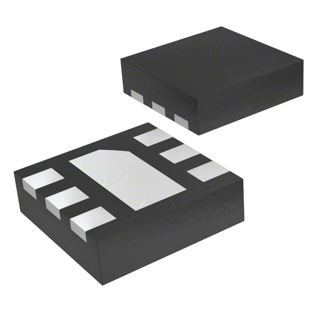
Available in WDFN6 2x2 mm Package
NCV Prefix for Automotive and Other Applications Requiring
Unique Site and Control Change Requirements; AEC−Q100
Qualified and PPAP Capable; Device Temperature Grade 1: −40°C to
+125°C Ambient Operating Temperature Range
These Devices are Pb−Free, Halogen Free/BFR Free and are RoHS
Compliant
WDFN6
MT SUFFIX
CASE 511BR
1
XX M
1
XX = Specific Device Code
M = Date Code
PIN CONNECTIONS
OUT
1
NC/ADJ
2
GND
3
GND
6
IN
5
NC
4
EN
WDFN6 2x2 mm
(Top View)
ORDERING INFORMATION
See detailed ordering and shipping information in the package
dimensions section on page 6 of this data sheet.
Typical Applications
•
•
•
•
•
•
Wireless Chargers
Portable Equipment
Communication Systems
In−Vehicle Networking
Telematics, Infotainment and Clusters
General Purpose Automotive
V IN
C IN
IN
V OUT
OUT
NCV8718
1 mF
Ceramic
EN
GND
NC
C OUT
1 mF
Ceramic
ON
OFF
Figure 1. Typical Application Schematic
© Semiconductor Components Industries, LLC, 2017
October, 2019 − Rev. 4
1
Publication Order Number:
NCV8718/D
�NCV8718
IN
IN
EN
ENABLE
LOGIC
BANDGAP
REFERENCE
EN
THERMAL
SHUTDOWN
BANDGAP
REFERENCE
MOSFET
DRIVER WITH
CURRENT LIMIT
INTEGRATED
SOFT−START
ENABLE
LOGIC
THERMAL
SHUTDOWN
MOSFET
DRIVER WITH
CURRENT LIMIT
INTEGRATED
SOFT−START
OUT
OUT
ADJ
* ACTIVE DISCHARGE
Version A only
* ACTIVE DISCHARGE
Version A only
EN
EN
GND
GND
Fixed Version
Adjustable Version
Figure 2. Simplified Block Diagram
Table 1. PIN FUNCTION DESCRIPTION
Pin No.
(WDFN6)
Pin Name
6
IN
3, EXP
GND
4
EN
2
NC / ADJ
Fixed Version: No connection. This pin can be tied to ground to improve thermal dissipation or left disconnected.
Adjustable Version: Feedback pin for set−up output voltage. Use resistor divider for voltage selection.
1
OUT
Regulated output voltage pin. A small 1 mF ceramic capacitor is needed from this pin to ground to assure
stability.
5
N/C
No connection. This pin can be tied to ground to improve thermal dissipation or left disconnected.
Description
Input pin. A small capacitor is needed from this pin to ground to assure stability.
Power supply ground.
Enable pin. Driving this pin high turns on the regulator. Driving EN pin low puts the regulator into shutdown mode.
Table 2. ABSOLUTE MAXIMUM RATINGS
Rating
Symbol
Value
Unit
Input Voltage (Note 1)
VIN
−0.3 to 24
V
Enable Voltage
VEN
−0.3 to VIN+0.3
V
Output Voltage
VOUT
−0.3 to VIN+0.3 (max. 6)
V
tSC
Indefinite
s
TJ(MAX)
150
°C
TSTG
−55 to 150
°C
ESD Capability, Human Body Model (Note 2)
ESDHBM
2000
V
ESD Capability, Charged Device Model (Note 2)
ESDCDM
1000
V
Output Short Circuit Duration
Maximum Junction Temperature
Storage Temperature
Stresses exceeding those listed in the Maximum Ratings table may damage the device. If any of these limits are exceeded, device functionality
should not be assumed, damage may occur and reliability may be affected.
1. Refer to ELECTRICAL CHARACTERISTICS and APPLICATION INFORMATION for Safe Operating Area.
2. This device series incorporates ESD protection and is tested by the following methods:
ESD Human Body Model tested per AEC−Q100−002 (EIA/JESD22−A114)
ESD Charged Device Model tested per EIA/JESD22−C101, Field Induced Charge Model.
Latch up Current Maximum Rating tested per JEDEC standard: JESD78. Latch−up is not guaranteed on ENABLE pin.
Table 3. RECOMMENDED OPERATING RANGES
Symbol
Min
Max
Unit
Input Voltage
Rating
VIN
2.5
24
V
Junction Temperature
TJ
−40
+125
°C
Functional operation above the stresses listed in the Recommended Operating Ranges is not implied. Extended exposure to stresses beyond
the Recommended Operating Ranges limits may affect device reliability.
www.onsemi.com
2
�NCV8718
Table 4. THERMAL CHARACTERISTICS
Rating
Symbol
Value
Unit
RqJA
65
°C/W
Thermal Characteristics, WDFN6, 2 mm x 2 mm
Thermal Resistance, Junction−to−Air
Table 5. ELECTRICAL CHARACTERISTICS -40°C ≤ TJ ≤ 125°C; VIN = 2.5 V or (VOUT + 1.0 V), whatever is greater; IOUT = 1 mA,
CIN = COUT = 1 mF, unless otherwise noted. Typical values are at TJ = +25°C. (Note 3)
Test Conditions
Symbol
VIN
−40°C ≤ TJ ≤ 125°C,
VOUT < 1.8 V
VOUT + 1 V < VIN < 16 V,
0.1 mA < IOUT < 300 mA (Note 5) VOUT ≥ 1.8 V
VOUT
−2%
+2%
Reference Voltage
−40°C ≤ TJ ≤ 125°C,
VOUT + 1 V < VIN < 16 V
VADJ
Reference Voltage Accuracy
−40°C ≤ TJ ≤ 125°C,
VOUT + 1 V < VIN < 16 V
VOUT
Line Regulation
VOUT + 1 V ≤ VIN ≤ 16 V, Iout = 1 mA
RegLINE
10
mV
Load Regulation
IOUT = 0.1 mA to 300 mA
RegLOAD
10
mV
VDO
490
mV
Parameter
Operating Input Voltage
Output Voltage Accuracy
(fixed versions)
Dropout Voltage
Maximum Output Current
Disable Current
Quiescent Current
Ground Current
Power Supply Rejection Ratio
Output Noise Voltage
Enable Input Threshold Voltage
VDO = VIN – (VOUT(NOM) – 3%),
IOUT = 300 mA (Note 4)
2.1 V – 2.4 V
Min
Typ
Max
Unit
2.5
24
V
−3%
+3%
V
1.2
−2%
+2%
2.5 V − 2.7 V
335
505
2.8 V − 3.2 V
305
475
3.3 V – 4.9 V
285
450
5V
260
395
VIN = VOUT + 1 V (Note 5)
ILIM
VEN = 0 V, VIN = 5 V
IDIS
IOUT = 0 mA, −40°C ≤ TJ ≤ 125°C
IOUT = 1 mA
300
mA
0.1
1.0
mA
IQ
4.0
8.0
mA
IGND
7.0
50
IOUT = 300 mA
300
f = 100 Hz
f = 1 kHz
f = 10 kHz
f = 100 kHz
V
800
IOUT = 10 mA
VIN = 3.5 V + 100 mVpp
VOUT = 2.5 V
IOUT = 1 mA, Cout = 1 mF
V
mA
PSRR
70
60
41
35
dB
VOUT = 1.2 V, IOUT = 10 mA
f = 100 Hz to 100 kHz
VN
36
mVrms
Voltage increasing
VEN_HI
1.2
−
−
−
V
Voltage decreasing
VEN_LO
−
0.4
ADJ Pin Current
VIN = VOUT + 1 V
IADJ
0.1
1.0
EN Pin Current
VEN = 5.5 V
IEN
100
nA
VIN = 5.5 V, VEN = 0 V
Rdis
100
W
Temperature increasing from TJ = +25°C
TSD
165
°C
Temperature falling from TSD
TSDH
Active Output Discharge
Resistance
Thermal Shutdown Temperature
(Note 6)
Thermal Shutdown Hysteresis
(Note 6)
−
25
−
mA
°C
Product parametric performance is indicated in the Electrical Characteristics for the listed test conditions, unless otherwise noted. Product
performance may not be indicated by the Electrical Characteristics if operated under different conditions.
3. Performance guaranteed over the indicated operating temperature range by design and/or characterization production tested at TJ = TA =
25°C. Low duty cycle pulse techniques are used during testing to maintain the junction temperature as close to ambient as possible.
4. Voltage dropout for voltage variants below 2.1 V is given by minimum input voltage 2.5 V.
5. Respect SOA
6. Guaranteed by design and characterization.
www.onsemi.com
3
�NCV8718
TYPICAL CHARACTERISTICS
1.212
1.208
1.204
IOUT = 1 mA
1.200
1.196
1.192
1.188
1.184
1.180
−40
1.0
IDIS, DISABLE CURRENT (mA)
4.0
VIN = 2.5 V
VOUT = 1.2 V
CIN = 1 mF
COUT = 1 mF
IQ, QUIESCENT CURRENT (mA)
1.216
−20
0
20
40
60
80
120
100
0.8
VIN = 24 V
0.3
VIN = 2.5 V
0.2
0.1
0
−40 −20
0
20
40
60
80
100
120
VOUT = 1.2 V
CIN = 1 mF
COUT = 1 mF
2.2
2.0
2
4
8
6
10
12
16
14
18
20
22 24
0.08
0.07
0.06
VEN = VIN
VOUT = 1.2 V
IOUT = 10 mA
CIN = 1 mF
COUT = 1 mF
0.05
VIN = 24 V
0.04
0.03
VIN = 2.5 V
0.02
−20
0
20
40
60
80
100
TJ, JUNCTION TEMPERATURE (°C)
TJ, JUNCTION TEMPERATURE (°C)
Figure 5. Disable Current vs. Temperature
Figure 6. Current to Enable Pin vs.
Temperature
ISC, SHORT CIRCUIT CURRENT (mA)
IGND, GROUND CURRENT (mA)
2.6
2.4
0.01
0
−40
30
VIN = 2.5 V
VOUT = 1.2 V
CIN = 1 mF
COUT = 1 mF
18
15
12
9
6
0
2.8
0.09
0.4
3
0
−40°C
3.0
0.10
0.5
21
25°C
3.2
Figure 4. Quiescent Current vs. Input Voltage
0.6
24
3.4
Figure 3. Output Voltage vs. Temperature −
VOUT = 1.2 V
0.7
27
125°C
3.6
VIN, INPUT VOLTAGE (V)
CIN = 1 mF
COUT = 1 mF
0.9
3.8
TJ, JUNCTION TEMPERATURE (°C)
IEN, ENABLE CURRENT (mA)
VOUT, OUTPUT VOLTAGE (V)
1.220
1
2
3
4
5
6
7
8
9
10
640
VIN = 2.5 V
VOUT = 1.2 V
CIN = 1 mF
COUT = 1 mF
620
600
580
560
540
520
500
480
460
440
−40 −20
0
20
40
60
80
100
IOUT, OUTPUT CURRENT (mA)
TJ, JUNCTION TEMPERATURE (°C)
Figure 7. Ground Current vs. Output Current −
VOUT = 1.2 V
Figure 8. Short Circuit Current vs.
Temperature
www.onsemi.com
4
120
120
�NCV8718
0.40
0.36
VDROP, DROPOUT VOLTAGE (V)
600
540
480
420
360
300
240
f = 50 Hz
Duty = 20%
CIN = 1 mF
COUT = 1 mF
180
120
60
0
0
2
4
6
8
10 12
14 16
18
22
20
24
0.24
0.16
0.12
0.08
0.04
0
Figure 9. SOA Current Limit vs. Differential
Voltage
Figure 10. Dropout Voltage vs. Output Current
− VOUT = 2.5 V
1 mA
70
60
10 mA
50
40
VIN = 3.5 V
VOUT = 2.5 V
CIN = 1 mF
COUT = 1 mF
MLCC, X7R, 0805
10
100
100 mA
1K
10K
100K
1M
10 mA
60
50
40
100 mA
VIN = 12 V
VOUT = 2.5 V
CIN = 1 mF
COUT = 1 mF
MLCC, X7R, 0805
30
20
10
10
100
1K
10K
100K
1M
10M
FREQUENCY (Hz)
FREQUENCY (Hz)
Figure 11. Power Supply Rejection Ratio vs.
Current, VIN = 3.5 V, COUT = 1 mF
Figure 12. Power Supply Rejection Ratio vs.
Current, VIN = 12 V, COUT = 1 mF
OUTPUT VOLTAGE NOISE (nV/√Hz)
100K
10K
1K
10
1 mA
70
0
10M
100K
100
0 0.04 0.08 0.12 0.16 0.20 0.24 0.28 0.32 0.36 0.40
IOUT, OUTPUT CURRENT (A)
80
10
−40°C
0.20
80
20
125°C
25°C
0.28
90
0
OUTPUT VOLTAGE NOISE (nV/√Hz)
0.32
90
30
VOUT = 2.5 V
CIN = 1 mF
COUT = 1 mF
VDIF, DIFFERENTIAL VOLTAGE VIN − VOUT (V)
RR, RIPPLE REJECTION (dB)
RR, RIPPLE REJECTION (dB)
SOA CURRENT LIMITATION (mA)
TYPICAL CHARACTERISTICS
VIN = 2.5 V
VOUT = 1.2 V
IOUT = 10 mA
CIN = 1 mF
COUT = 1 mF
MLCC, X7R, 0805
10
100
1K
10K
100K
1M
10K
1K
VIN = 2.8 V
VOUT = 1.8 V
IOUT = 10 mA
CIN = 1 mF
COUT = 1 mF
MLCC, X7R, 0805
100
10
10
100
1K
10K
100K
FREQUENCY (Hz)
FREQUENCY (Hz)
Figure 13. Output Voltage Noise Spectral
Density for VOUT = 1.2 V, IOUT = 10 mA,
COUT = 1 mF
Figure 14. Output Voltage Noise Spectral
Density for VOUT = 1.8 V, IOUT = 10 mA,
COUT = 1 mF
www.onsemi.com
5
1M
�NCV8718
APPLICATIONS INFORMATION
Power Dissipation and Heat Sinking
The NCV8718 is the member of new family of Wide Input
Voltage Range Low Dropout Regulators which delivers
Ultra Low Ground Current consumption, Good Noise and
Power Supply Rejection Ratio Performance. The NCV8718
incorporates EN pin and soft−start feature for simple
controlling by microprocessor or logic.
The maximum power dissipation supported by the device
is dependent upon board design and layout. Mounting pad
configuration on the PCB, the board material, and the
ambient temperature affect the rate of junction temperature
rise for the part. For reliable operation junction temperature
should be limited to +125°C.
The maximum power dissipation the NCV8718 can
handle is given by:
Input Decoupling (CIN)
It is recommended to connect at least 1 mF ceramic X5R
or X7R capacitor between IN and GND pin of the device.
This capacitor will provide a low impedance path for any
unwanted AC signals or noise superimposed onto constant
input voltage. The good input capacitor will limit the
influence of input trace inductances and source resistance
during sudden load current changes.
Higher capacitance and lower ESR capacitors will
improve the overall line transient response.
P D(MAX) +
ƪTJ(MAX) * TAƫ
(eq. 1)
R qJA
The power dissipated by the NCV8718 for given
application conditions can be calculated from the following
equations:
P D [ V INǒI GND(I OUT)Ǔ ) I OUTǒV IN * V OUTǓ
(eq. 2)
or
Output Decoupling (COUT)
The NCV8718 does not require a minimum Equivalent
Series Resistance (ESR) for the output capacitor. The device
is designed to be stable with standard ceramics capacitors
with values of 1 mF or greater. The X5R and X7R types have
the lowest capacitance variations over temperature thus they
are recommended.
V IN(MAX) [
P D(MAX) ) ǒV OUT
I OUTǓ
I OUT ) I GND
(eq. 3)
Hints
VIN and GND printed circuit board traces should be as
wide as possible. When the impedance of these traces is
high, there is a chance to pick up noise or cause the regulator
to malfunction. Place external components, especially the
output capacitor, as close as possible to the NCV8718, and
make traces as short as possible.
ORDERING INFORMATION
Device Part No.
Voltage Option
Marking
NCV8718AMTADJTBG
Adj.
GA
NCV8718AMT180TBG
1.8 V
GP
NCV8718AMT300TBG
3.0 V
GQ
NCV8718AMT330TBG
3.3 V
GR
NCV8718AMT500TBG
5.0 V
GM
NCV8718BMTADJTBG
Adj.
GC
NCV8718BMT180TBG
1.8 V
GU
NCV8718BMT300TBG
3.0 V
GV
NCV8718BMT330TBG
3.3 V
GW
NCV8718BMT500TBG
5.0 V
GE
Option
Package
Shipping†
WDFN6
(Pb−Free)
3000 / Tape & Reel
With Active Output
Discharge
Without Active Output
Discharge
†For information on tape and reel specifications, including part orientation and tape sizes, please refer to our Tape and Reel Packaging
Specifications Brochure, BRD8011/D.
www.onsemi.com
6
�MECHANICAL CASE OUTLINE
PACKAGE DIMENSIONS
WDFN6 2x2, 0.65P
CASE 511BR
ISSUE C
DATE 01 DEC 2021
GENERIC
MARKING DIAGRAM*
1
XX M
XX = Specific Device Code
M = Date Code
*This information is generic. Please refer to
device data sheet for actual part marking.
Pb−Free indicator, “G” or microdot “G”, may
or may not be present. Some products may
not follow the Generic Marking.
DOCUMENT NUMBER:
DESCRIPTION:
98AON55829E
WDFN6 2X2, 0.65P
Electronic versions are uncontrolled except when accessed directly from the Document Repository.
Printed versions are uncontrolled except when stamped “CONTROLLED COPY” in red.
PAGE 1 OF 1
onsemi and
are trademarks of Semiconductor Components Industries, LLC dba onsemi or its subsidiaries in the United States and/or other countries. onsemi reserves
the right to make changes without further notice to any products herein. onsemi makes no warranty, representation or guarantee regarding the suitability of its products for any particular
purpose, nor does onsemi assume any liability arising out of the application or use of any product or circuit, and specifically disclaims any and all liability, including without limitation
special, consequential or incidental damages. onsemi does not convey any license under its patent rights nor the rights of others.
© Semiconductor Components Industries, LLC, 2019
www.onsemi.com
�onsemi,
, and other names, marks, and brands are registered and/or common law trademarks of Semiconductor Components Industries, LLC dba “onsemi” or its affiliates
and/or subsidiaries in the United States and/or other countries. onsemi owns the rights to a number of patents, trademarks, copyrights, trade secrets, and other intellectual property.
A listing of onsemi’s product/patent coverage may be accessed at www.onsemi.com/site/pdf/Patent−Marking.pdf. onsemi reserves the right to make changes at any time to any
products or information herein, without notice. The information herein is provided “as−is” and onsemi makes no warranty, representation or guarantee regarding the accuracy of the
information, product features, availability, functionality, or suitability of its products for any particular purpose, nor does onsemi assume any liability arising out of the application or use
of any product or circuit, and specifically disclaims any and all liability, including without limitation special, consequential or incidental damages. Buyer is responsible for its products
and applications using onsemi products, including compliance with all laws, regulations and safety requirements or standards, regardless of any support or applications information
provided by onsemi. “Typical” parameters which may be provided in onsemi data sheets and/or specifications can and do vary in different applications and actual performance may
vary over time. All operating parameters, including “Typicals” must be validated for each customer application by customer’s technical experts. onsemi does not convey any license
under any of its intellectual property rights nor the rights of others. onsemi products are not designed, intended, or authorized for use as a critical component in life support systems
or any FDA Class 3 medical devices or medical devices with a same or similar classification in a foreign jurisdiction or any devices intended for implantation in the human body. Should
Buyer purchase or use onsemi products for any such unintended or unauthorized application, Buyer shall indemnify and hold onsemi and its officers, employees, subsidiaries, affiliates,
and distributors harmless against all claims, costs, damages, and expenses, and reasonable attorney fees arising out of, directly or indirectly, any claim of personal injury or death
associated with such unintended or unauthorized use, even if such claim alleges that onsemi was negligent regarding the design or manufacture of the part. onsemi is an Equal
Opportunity/Affirmative Action Employer. This literature is subject to all applicable copyright laws and is not for resale in any manner.
PUBLICATION ORDERING INFORMATION
LITERATURE FULFILLMENT:
Email Requests to: orderlit@onsemi.com
onsemi Website: www.onsemi.com
◊
TECHNICAL SUPPORT
North American Technical Support:
Voice Mail: 1 800−282−9855 Toll Free USA/Canada
Phone: 011 421 33 790 2910
Europe, Middle East and Africa Technical Support:
Phone: 00421 33 790 2910
For additional information, please contact your local Sales Representative
�


 工商网监
湘ICP备2023018690号
工商网监
湘ICP备2023018690号
