Low Quiescent Current
410�kHz Automotive
Synchronous Buck Controller
NCV881930
www.onsemi.com
1 24
QFNW24 4x4, 0.5P
CASE 484AE
Note: With wettable flanks – meets JEDEC MO220
MARKING DIAGRAM
1
24
ZZZZZ
30XX
ALYWG
G
(2 MHz version offered with NCV891930)
Features
*For additional information on our Pb−Free strategy and soldering details, please
download the ON Semiconductor Soldering and Mounting Techniques
Reference Manual, SOLDERRM/D.
© Semiconductor Components Industries, LLC, 2018
April, 2020 − Rev. 3
1
PIN CONNECTIONS
GH
VSW
GL
PGND
24
23
22
21
20
VCCEXT
BST
(Top View)
19
18
V_CS
1
CSP
2
17
VIN
CSN
3
16
DBIAS
VOUT
4
15
VSEL
NC
5
14
V_SO
EN
6
GND
7
8
9
10
11
13
12
SYNCI
Radio and Infotainment
Instrumentations & Clusters
ADAS (safety applications)
Telematics
(Note: Microdot may be in either location)
RSTB
•
•
•
•
= V8819, 8819A
= 00
= Assembly Location
= Wafer Lot
= Year
= Work Week
= Pb−Free Package
SSC
Typical Applications
ZZZZZ
XX
A
L
Y
W
G
ROSC
•
30 mA Operating Current at No Load
50 mV Current Limit Sensing
Capable of 45 V Load Dump
Board Selectable Fixed Output Voltages with Lockout
410 kHz Operating Frequency
Adaptive Non−Overlap Circuitry
Integrated Spread Spectrum
Logic level Enable Input Can be Tied Directly to Battery
Short Circuit Protection Pulse Skip
Battery Monitoring for UVLO and Overvoltage Protection
Thermal Shutdown (TSD)
Adjustable Soft−Start
SYNCI, SYNCO, Enable, RSTB, ROSC
QFN Package with Wettable Flanks (pin edge plating)
NCV Prefix for Automotive and Other Applications Requiring
Unique Site and Control Change Requirements; AEC−Q100
This Device is Pb−Free, Halogen Free/BFR Free and is RoHS
Compliant
NC
•
•
•
•
•
•
•
•
•
•
•
•
•
•
•
GND
The NCV881930 is a 410 kHz fixed−frequency low quiescent
current buck controller with spread spectrum that operates up to 38 V
(typical). It may be synchronized to a clock or to separate
NCV881930. Peak current mode control is employed for fast transient
response and tight regulation over wide input voltage and output load
ranges. Feedback compensation is internal to the device, permitting
design simplification. The NCV881930 is capable of converting from
an automotive input voltage range of 3.5 V (4.5 V during startup) to
18 V at a constant base switching frequency. Under load dump
conditions up to 45 V the regulator shuts down. A high voltage bias
regulator with automatic switchover to an external 5 V bias supply is
used for improved efficiency. Several protection features such as
UVLO, current limit, short circuit protection, and thermal shutdown
are provided. High switching frequency produces low output voltage
ripple even when using small inductor values and an all−ceramic
output filter capacitor, forming a space−efficient switching solution.
VDRV
SYNCO
ORDERING INFORMATION
See detailed ordering and shipping information on page 27 of
this data sheet.
Publication Order Number:
NCV881930/D
�NCV881930
SYNCI
V_CS
CSP
1
24
NCV881930
8
23
9
22
10
21
GND
11
20
12
13
SYNCO
RSYNCI
+
V IN
−
14
15
16
19
18
17
BST
GH
Q1
RS
VSW
GL
NVMFS5C460NL
C BST
Q2
L
NVMFS5C460NL
+
C
VOUT
PGND
−
VCCEXT
VDRV
RSTB
VOUT
2
VIN
GND
3
DBIAS
SSC
4
VSEL
ROSC
5
V_SO
ROSC
6
7
CSN
NC
EN
NC
VOUT
V IN
V IN
Figure 1. 5 V Application Schematic Example
RSTB
SYNCI
R SYNCI
V_CS
CSP
CSN
VOUT
NC
+
VIN
−
1
24
NCV881930
8
23
9
22
10
GH
GL
15
16
RS
Q2
L
NVMFS5C460NL
VIN
Figure 2. 3.3 V Application Schematic Example
2
+
−
Open
or +5V
www.onsemi.com
C
VOUT
VCCEXT
19
18
17
NVMFS5C460NL
CBST
PGND
20
14
Q1
VSW
21
GND
11
12
13
BST
VDRV
VOUT
2
VIN
GND
3
DBIAS
SSC
4
VSEL
R OSC
5
V_SO
ROSC
6
7
SYNCO
NC
EN
V IN
�NCV881930
13
SYNCI
12
ROSC
8
VCCEXT
VDRV
BST
17
19
18
24
LDO
BYPASS
5 V LDO
S
R
OSC
14
DBIAS
16
V_CS
1
EN
6
NON
OVERLAP
Q
PWMOUT
INTERNAL
RAILS
SYNCI
FB
GH
VDRV
22
VSW
21
GL
20
PGND
2
CSP
3
CSN
4
VOUT
15
VSEL
Current Limit
VNCL
PWM/
PULSE SKIP
BANDGAP
VPCL
SLOPE
COMP
TSD
OVSD
UVLO
FAULT
SOFTSTART
23
MIN
ON TIME
CSA
∑
VREF
VCOMP
FB
−
V_SO
Q
+
SYNC0
VIN
Z
RSTB
9
10
11
SSC
GND
RSTB
Figure 3. Simplified Block Diagram
www.onsemi.com
3
�NCV881930
Table 1. PIN FUNCTION DESCRIPTION
Pin No.
QFN24
Pin Name
Description
1
V_CS
Supply input for the internal current sense amplifier. Not intended for external use. Application
board requires a 0.1 mF decoupling capacitor located next to IC referenced to quiet GND.
2
CSP
Differential current sense amplifier non−inverting input.
3
CSN
Differential current sense amplifier inverting input.
4
VOUT
5
NC
No connection (Note 1)
6
EN
Logic level inputs for enabling the controller. May be connected to battery.
7
NC
No Connection (Note 1)
8
ROSC
9
SSC
Soft−start current source output. A capacitor to ground sets the soft−start time.
10
GND
Signal ground. Ground reference for the internal logic, analog circuitry and the compensators.
11
RSTB
Reset with adjustable delay. Goes low when the output is out of regulation.
12
SYNCI
A logic low enables Low IQ capable operating mode. External synchronization is realized with
an external clock. A logic high enables continuous synchronous operating mode (low IQ mode
is disabled). Ground this pin if not used.
13
SYNCO
Synchronization output active in synchronous operation mode. Refer to table for activation
delay when coming out of low IQ mode. Connecting to the SYNCI pin of a downstream
NCV881930 results in synchronized operation.
14
V_SO
Supply voltage for the SYNCO output driver. Not intended for external use. Application board
requires a 0.1 mF decoupling capacitor located next to IC referenced to quiet GND.
15
VSEL
Output programmed to VSEL_LO when connected to ground or when pin is not connected.
Output programmed to VSEL_HI when connected to DBIAS via a 10 kW resistor (optional).
Voltage setting option will be latched prior to PWM soft−start. Latch will be reset whenever the
EN pin is toggled or during a UVLO event.
16
DBIAS
IC internal power rail. Not intended for external use other than for VSEL. Application board
requires a 0.1 mF decoupling capacitor located next to IC referenced to quiet GND.
17
VIN
18
VDRV
19
VCCEXT
External 5 V bias supply. Overrides internal high voltage LDO when used. Application board
requires a 1 mF decoupling capacitor located next to IC referenced to PGND.
20
PGND
Power ground. Ground reference for the high−current path including the N−FETs and output
capacitor.
21
GL
Push−pull driver output that swings between VDRV and PGND to drive the gate of an external
low side N−FET of the synchronous buck power supply.
22
VSW
Terminal of the high side push−pull gate driver connected to the source of the high side N−FET
of the synchronous buck power supply.
23
GH
Push−pull driver output that swings between SW and BST to drive the gate of an external high
side N−FET of the synchronous buck power supply.
24
BST
The BST pin is the supply rail for the gate drivers. A 0.1 mF capacitor must be connected between this pin and the VSW pin. Bootstrap pin to be connected with an external capacitor for
powering the high side NFET gate with SW + (VDRV – 0.5 V) and PGND. Blocking diode is
internal to the IC.
EPAD
SMPS’s voltage feedback. Inverting input to the voltage error amplifier. Connect VOUT to
nearest point−of−load.
Use a resistor to ground to raise the frequency above default value.
Input voltage for controller, may be connected to battery.
5 V linear regulator supply for powering NFET gate drive circuitry and supply for bootstrap
capacitor.
Connect to pin 20 (electrical ground) and to a low thermal resistance path to the environment.
1. True no connect. Printed circuit board traces are allowable.
www.onsemi.com
4
�NCV881930
Table 2. MAXIMUM RATINGS (Voltages with respect to GND unless otherwise indicated)
Rating
Symbol
Value
Unit
EN, VIN, V_CS
−0.3 to 45
V
Pin Voltage
t ≤ 50 ns
VSW
−0.3 to 40
−2
V
Pin Voltage
GH, BST
−0.3 to 45
−0.3 to 7 V with respect to VSW
V
Pin Voltage
CSN, CSP, VOUT
−0.3 to 10
V
Pin Voltage
VDRV, GL, VCCEXT
−0.3 to 7
V
Pin Voltage
RSTB, SYNCI
−0.3 to 6
V
Pin Voltage
DBIAS, ROSC, SSC,
SYNCO, V_SO, VSEL
−0.3 to 3.6
V
TJ(max)
−40 to 150
°C
TSTG
−65 to 150
°C
ESDHBM
2
kV
Moisture Sensitivity Level
MSL
1
−
Lead Temperature Soldering
Reflow (SMD Styles Only), Pb−Free Versions (Note 4)
TSLD
260
°C
DC Supply Voltage (Note 2)
Operating Junction Temperature
Storage Temperature Range
ESD Capability, Human Body Model (Note 3)
Stresses exceeding those listed in the Maximum Ratings table may damage the device. If any of these limits are exceeded, device functionality
should not be assumed, damage may occur and reliability may be affected.
2. Refer to ELECTRICAL CHARACTERISTICS, RECOMMENDED OPERATING RANGES and/or APPLICATION INFORMATION for Safe
Operating parameters.
3. This device series incorporates ESD protection and is tested by the following methods:
ESD Human Body Model tested per AEC−Q100−002 (EIA/JESD22−A114).
4. For information, please refer to our Soldering and Mounting Techniques Reference Manual, SOLDERRM/D.
Table 3. THERMAL CHARACTERISTICS
Rating
Symbol
Value
RθJA
yJT
50
13
Thermal Characteristics (Note 5)
Thermal Resistance, Junction−to−Ambient (Note 6)
Thermal Characterization Parameter, Junction−to−Top (Note 6)
Unit
°C/W
5. Refer to ELECTRICAL CHARACTERISTICS, RECOMMENDED OPERATING RANGES and/or APPLICATION INFORMATION for Safe
Operating parameters.
6. Values based on copper area of 600 mm2, 4 layer PCB, 0.062 inch FR−4 board with 2 oz. copper on top/bottom layers and 1 oz. copper on
the inside layers in a still air environment with TA = 25°C.
Table 4. ELECTRICAL CHARACTERISTICS
(VEN = VBAT = VIN = 4.5 V to 37 V, VBST = VSW + (VDRV – 0.5 V), CBST = 0.1 mF, CDRV = 1 mF. Min/Max values are valid for the
temperature range −40°C < TJ < 150°C unless noted otherwise, and are guaranteed by test, design or statistical correlation.
Parameter
Test Conditions
Symbol
Min
Typ
Max
Unit
VINLF
VINLR
7.0
7.3
7.31
7.65
7.65
8.0
V
VINLH
0.25
0.32
0.45
V
−
5.8
−
ms
VINHR
VINHF
18.4
18.0
−
−
20
19.8
V
VFLHY
0.15
0.32
0.45
V
−
16
−
ms
VIN_LOW
VIN_low threshold
VIN falling
VIN rising
VIN_low hysteresis
Response time
SPREAD SPECTRUM DEACTIVATION (VIN_HIGH)
VIN_high threshold
VIN rising
VIN falling
VIN_high hysteresis
Response time
www.onsemi.com
5
�NCV881930
Table 4. ELECTRICAL CHARACTERISTICS
(VEN = VBAT = VIN = 4.5 V to 37 V, VBST = VSW + (VDRV – 0.5 V), CBST = 0.1 mF, CDRV = 1 mF. Min/Max values are valid for the
temperature range −40°C < TJ < 150°C unless noted otherwise, and are guaranteed by test, design or statistical correlation.
Parameter
Test Conditions
Symbol
Min
Typ
Max
Unit
Overvoltage stop threshold
VOVSP
37.0
38.0
39.0
V
Overvoltage hysteresis
VOVHY
0.5
1.0
1.5
V
IQ,SLEEP
−
6.0
−
mA
IQ,SLEEP
−
6.0
10
mA
VIN = 13 V, EN = 5 V, No switching,
TJ = 25°C
IQ,OFF
−
30
40
mA
VIN = 13 V, 100 mA load, VOUT = 5 V,
VCCEXT = VOUT, EN = VIN,
Tambient = 25°C
(Not production tested. Measured on demo
board, refer to application note section)
IQ100
−
82
100
mA
VDBIAS
2.0
−
2.4
V
VIN OVERVOLTAGE SHUTDOWN MONITOR
QUIESCENT CURRENT
Quiescent current
VIN = 13 V, EN = 0 V, TJ = 25°C
VIN = 13 V, EN = 0 V, −40°C < TJ <
125°C
DBIAS
DBIAS voltage
CDBIAS = 0.1 mF
UNDERVOLTAGE LOCKOUT (Note 8)
UVLO start threshold
VIN rising
VUVST
4.0
−
4.5
V
UVLO stop threshold
VIN falling
VUVSP
3.2
−
3.5
V
VUVHY
−
0.9
−
V
UVLO hysteresis
ENABLE
Logic low threshold voltage
Will be disabled at maximum value
VENLO
0
−
0.8
V
Logic high threshold voltage
Will be enabled at minimum value
VENHI
1.4
−
−
V
Enable pin input Current
VEN = 5 V
EI,EN
−
0.125
0.26
mA
OUTPUT VOLTAGE
Output voltage during regulation
VOUT,REG
IOUT > 100 mA
NCV881930MW00R2G/A2RG
3.3 V (VSEL = GND)
5.0 V (VSEL = DBIAS)
V
3.234
4.90
3.30
5.00
3.366
5.10
RENLO,VOUT
70
100
130
W
VSEL input low threshold
voltage
VLVSEL
0
−
0.8
V
VSEL input high threshold
voltage
VHVSEL
2.0
−
3.3
V
VSEL = DBIAS
VI,SEL
−
0.25
0.37
mA
VOUT decreasing
VOUT increasing
KUVFAL
KUVRIS
90
90.5
92.5
−
95
97
%
Reset hysteresis (ratio of VOUT)
KRES_HYS
0.5
−
2
%
Noise−filtering delay
tRES_FILT
5
−
25
ms
tRESET
−
4
17
1.0
5
24
−
6
32
ms
ms
ms
1000
−
−
−
−
600
mA
VOUT−GND resistance
EN = VENLO, VIN > 4.5 V
VSEL
VSEL pin input current
RESET
Reset threshold 1
(as a function of VOUT)
Reset delay time
IRSTB = 1 mA
IRSTB = 500 mA
IRSTB = 100 mA
Reset delay modes
Power good mode (no delay)
Delay mode
(see Detailed Operating Description)
www.onsemi.com
6
�NCV881930
Table 4. ELECTRICAL CHARACTERISTICS
(VEN = VBAT = VIN = 4.5 V to 37 V, VBST = VSW + (VDRV – 0.5 V), CBST = 0.1 mF, CDRV = 1 mF. Min/Max values are valid for the
temperature range −40°C < TJ < 150°C unless noted otherwise, and are guaranteed by test, design or statistical correlation.
Parameter
Test Conditions
Symbol
Min
Typ
Max
Unit
RESET
Reset output low level
IRSTB = 1 mA
VRESL
−
−
0.4
V
Reset threshold 2
(as a function of VOUT)
VOUT increasing
VOUT decreasing
KOVRIS
KOVFAL
105
104
106.5
106.5
110
109
%
VOUT Output Clamp Current
VOUT = VOUT,reg(typ) + 10%
ICL,OUT
0.5
1.0
1.5
mA
gM,OTA
−
26.6
−
ERROR AMPLIFIER
Transconductance (Note 3)
Internal to IC
Compensation network
Internal to IC
NCV881930MW00DRG
3.3 V
5.0 V
RCOMP,OTA
Internal to IC
(refer to application note section for die
distributed capacitance modeling information)
Internal to IC
Slope compensation
mS
kW
−
−
293
347
−
−
CCOMP,OTA
−
190
−
pF
R0,OTA
−
56.7
−
MW
Sa
−
4.1
−
mV/ms
fSW
369
410
451
kHz
OSCILLATOR
Switching frequency
4.5 V < VIN < VOVSP, ROSC = open
Switching frequency – ROSC
4.5 V < VIN < VINHR/VINHF, ROSC = 9.01 kW
fROSC
471
512
574
kHz
ROSC reference voltage
ROSC = 9.01 kW
VROSC
0.36
0.40
0.44
V
tOFF,MIN
−
49
75
ns
fMOD
fsw
−
fsw+14%
kHz
Minimum off time
SPREAD SPECTRUM
Modulation Frequency Range
VINLF/VINLR < VIN < VINHR/VINHF
SYNCHRONIZATION
SYNCO output pulse duty ratio
CLOAD = 40 pF, SYNCI = 0 or SYNCI = 1
D(SYNC)
40
−
60
%
SYNCO output pulse fall time
CLOAD = 40 pF, 90% to 10%
tR(SYNC)
−
4.7
−
ns
SYNCO output pulse rise time
CLOAD = 40 pF, 10% to 90%
tF(SYNC)
−
7.0
−
ns
SYNCO Logic High
ISYNCO = 100 mA source current
VSYNCOHI
2.2
−
3.45
V
SYNCO Logic Low
ISYNCO = 2 mA sink current
VSYNCOLO
−
−
0.4
V
SYNCI pull−down resistance
RSYNCI
50
100
200
kW
SYNCI input low threshold
voltage
VLSYNCI
0
−
0.8
V
SYNCI input high threshold
voltage
VHSYNCI
2.0
−
5.5
V
SYNCI high pulse width
tHSYNCI
100
−
−
ns
External SYNCI Frequency
fSYNCI
369
−
512
kHz
Master Reassertion Time
Time from last rising SYNCI edge to first un−
synchronized turn−on.
SYNCI = VLSYNCI after falling SYNCI edge
SYNCI = VHSYNCI after falling SYNCI edge
tl(SYNC)
ms
−
−
6.10
8.54
−
−
SOFT−START CURRENT
Soft−start charge current
ISS
6.9
10
14.3
mA
Soft−start complete threshold
VSS
−
1.0
−
V
www.onsemi.com
7
�NCV881930
Table 4. ELECTRICAL CHARACTERISTICS
(VEN = VBAT = VIN = 4.5 V to 37 V, VBST = VSW + (VDRV – 0.5 V), CBST = 0.1 mF, CDRV = 1 mF. Min/Max values are valid for the
temperature range −40°C < TJ < 150°C unless noted otherwise, and are guaranteed by test, design or statistical correlation.
Parameter
Test Conditions
Symbol
Min
Typ
Max
Unit
From EN = 1 until start of charging of soft−
start capacitor
(DBIAS external capacitor = 0.1 mF)
tSSDLY
−
240
−
ms
0 ≤ (CSP – CSN) ≤ 200 mV
1.2 V ≤ CSN ≤ 10.0 V, VIN < VIN_HIGH
VPCL,N
45
50
55
mV
0 ≤ (CSP – CSN) ≤ 200 mV
1.2 V ≤ CSN ≤ 10.0 V, VIN > VINH
(Guaranteed by design)
VPCL,H
48
53.3
58.7
mV
tCL
−
39
125
ns
VNCL
−20.5
−35.0
−52.0
mV
Common−mode range
−
VOUT
−
V
CSP input bias source current
−
0.1
1.0
mA
IBIAS,CSN
−
30
−
mA
SOFT−START CURRENT
Soft−start delay
PEAK CURRENT LIMITS
Positive current limit threshold
voltage
Current limit response time
Comparator tripped until GH falling edge,
(VCSP – VCSN) = VCL(typ) + 5 mV
Negative current limit threshold
voltage
−200 mV ≤ (CSP – CSN) ≤ 0
1.2 V ≤ CSN ≤ 10.0 V
CSN input bias source current
GATE DRIVERS
GH sourcing ON resistance
VBST – VGH = 2 V
RGHSOURCE
1.6
2.5
5.3
W
GH sinking ON resistance
VGH – VSW = 2 V
RGHSINK
1.3
2.5
4.3
W
RGH,VSW
−
20
−
kW
RGLSOURCE
1.6
2.5
5.3
W
RGLSINK
1.3
2.5
4.3
W
RGL,PGND
−
20
−
kW
VDRV,DO
−
0.3
0.6
V
IDRV
65
100
−
mA
GH−VSW resistance
GL sourcing ON resistance
VVDRV – VGL = 2 V
GL sinking ON resistance
VGL = 2 V
GL−PGND resistance
GATE DRIVE SUPPLY
Driving voltage dropout
VIN – VDRV, IVDRV = 25 mA
Driving voltage source current
VIN – VDRV = 1 V
Backdrive diode voltage drop
VDRV – VIN, Id,bd = 5 mA
VD,BD
−
−
0.7
V
Driving voltage
IVDRV = 0.1 – 25 mA
VDRV
4.75
5.00
5.30
V
VDRV POR start threshold
(Note 8)
VDRVST
3.75
4.0
4.25
V
VDRV POR stop threshold
(Note 8)
VDRVSP
2.85
3.1
3.35
V
LDO bypass start threshold
VCCEXT rising
4.48
−
4.80
V
LDO bypass stop threshold
VCCEXT falling
4.31
−
4.65
V
LDO bypass input current
Pulse−skip, VCCEXT = 5 V
−
3.1
−
mA
LDO bypass RDS(on)
VCCEXT = 5 V, VDRV load = 50 mA
1.07
1.93
2.79
W
THERMAL SHUTDOWN
Thermal shutdown threshold
TJ rising
TSD
155
170
190
°C
Thermal shutdown hysteresis
TJ falling
TSD,HYS
5
15
20
°C
Product parametric performance is indicated in the Electrical Characteristics for the listed test conditions, unless noted. Product
performance may not be indicated by the Electrical Characteristics if operated under different conditions.
7. Spread spectrum function will be disabled when IC operated using external frequency synchronization.
8. Operating with VIN near IC UVLO thresholds may result in insufficient gate drive voltage drive amplitude to permit switching of external
MOSFETs. Use of an external bias voltage to maintain sufficient VDRV voltage may be required.
www.onsemi.com
8
�NCV881930
Table 5. FUNCTIONALITY INFORMATION TABLE
VIN (V)
SYNCI
Pin
VIN < Vin_low
Logic−0
Logic−1
Fsync
Vin_low < VIN
< Vin_high
(No Pulse Skip
Condition)
Logic−0
Logic−1
Fsync
SYNCI
Function
Behavior
Frequency
SYNCO
Synchronous mode, recirculation FET turns−off when
−35 mV current sense voltage is detected.
Pulse skip not allowed when
VIN < Vin_low.
410 kHz* or less. Minimum off−
time may be skipped depending
on VIN, output voltage option
and operating current.
Disabled
Enabled,
410 kHz
Fsync if minimum off−time is
not skipped
Enabled
Fsync
Synchronous mode, recirculation FET turns−off when
when < 0 V current sense
voltage is detected.
fROSC with spread spectrum.
Disabled
Enabled,
follows
spread
spectrum
Upon exiting Pulse Skip mode,
first 1−3 pulses 103 kHz followed by 410 kHz pulses.
Spread
Spectrum
ROSC
Disabled
Disabled
Enabled
Enabled
(When exiting
(Disabled
Pulse Skip
during
mode, function 1−3 103 kHz
resumes within pulses upon
14 410 kHz
exiting Pulse
pulses)
Skip mode)
Forced PWM mode, recirculation FET turns−off when
−35 mV current sense voltage is detected.
fROSC with spread spectrum
Disabled
Enabled
Enabled
Enabled
Fsync
Enabled
Fsync
Disabled
Disabled
Vin_low < VIN <
Vin_high (Pulse
Skip Condition)
Logic−0
Pulse skip mode
Disabled
Disabled
Disabled
Disabled
Disabled
VIN > Vin_high
X
Synchronous mode, recirculation FET turns−off when
−35 mV current sense voltage is detected.
Pulse skip not allowed when
VIN > Vin_high.
410 kHz
Disabled
Enabled,
410 kHz
Disabled
Disabled
Soft−start
X
Forced PWM mode with
pulse skip allowed, recirculation FET turns−off when
when < 0 V current sense
voltage is detected.
410 kHz
Disabled
Disabled
Disabled
Disabled
Vout undervoltage (KUV)
X
RSTB activated
410 kHz
No change
in behavior
No change in
behavior
Disabled
No change in
behavior
Vout overvoltage (KOV)
X
RSB activated
No PWM
No PWM
No Change
in behavior
No PWM
No PWM
*GH off pulses will be skipped to maintain output voltage regulation whenever GH toff is less than toff,MIN occurs.
THERMAL CHARACTERISTICS
1
60
Rise Time (ns)
CSS (mF)
50
0.1
GL
GH
40
30
20
10
0.01
1
10
tSS (ms)
100
0
0
2
4
6
8
10
Load Capacitance (nF)
Figure 4. Soft−Start Time vs Capacitance
Figure 5. Driver Rise Time vs Load Capacitance
www.onsemi.com
9
�NCV881930
THERMAL CHARACTERISTICS
45
40
GL
GL
GH
GH
30
25
I (mA)
Q
Fall Time (ns)
35
20
15
10
5
0
0
2
4
6
Load Capacitance (nF)
8
10
90
85 VCCEXT = OPEN
80
75
70
65
60
55
50
45
40
35
30
25
−50 −25
0
25
50
75
Temperature (°C)
100
125
150
Figure 7. Operating Quiescent Current vs
Temperature (5 V/100 mA)
Figure 6. Driver Fall Time vs Load Capacitance
10
53
9
52
8
VCSP,CSN (mV)
IQ,SLEEP (mA)
7
6
5
4
3
2
51
50
49
48
1
0
−50
−25
0
25
50
75
100
47
−50
125
−25
0
25
Temperature (°C)
409
100.3%
408
Switching Frequency (kHz)
410
100.4%
100.2%
VREF
100.1%
100.0%
99.9%
99.8%
99.7%
99.6%
0
25
50
75
Temperature (°C)
100
125
Figure 9. Peak Current−Limit Threshold vs
Temperature
100.5%
−25
75
Temperature (°C)
Figure 8. Quiescent Current (Shutdown) vs
Temperature
99.5%
−50
50
100
407
406
405
404
403
402
401
400
−50
125
Figure 10. VREF vs Temperature
−25
0
25
50
Temperature (°C)
75
100
125
Figure 11. Oscillator Frequency vs Temperature
www.onsemi.com
10
�NCV881930
THERMAL CHARACTERISTICS
4.4
29
Non Overlap Delay (ns)
27
GH: High to Low
4.3
GL: Low to High
4.2
4.1
25
23
VIN RISING
V
3.9
3.8
21
3.7
GH: Low to High
19
3.6
GL: High to Low
3.5
17
3.4
15
−50
−25
0
25
50
Temperature (°C)
75
100
3.3
−50
125
Figure 12. Non−Overlap Delay vs Temperature
−25
0
5.06
125
20
18
tRESET (ms)
5.02
5.00
4.98
4.96
16
14
12
10
4.94
8
4.92
6
4.90
−50
4
−25
0
25
50
75
100
125
0.1
0.2
Temperature (°C)
VIN=6V
VIN=16V
100
VIN=8V
VIN=18V
VIN=10V
VIN=20V
VIN=12V
VIN=22V
VIN=14V
VIN=34V
VIN=6V
VIN=16V
100
80
80
70
70
E FF (%)
90
60
50
40
0.5
VIN=12V
VIN=22V
VIN=14V
VIN=34V
40
20
20
10
10
0
10000
VIN=10V
VIN=20V
50
30
1000
VIN=8V
VIN=18V
60
30
1
10
100
Output Current (mA)
0.4
Figure 15. Reset Delay Time vs IRSTBx
90
0.1
0.3
IRSTBx (mA)
Figure 14. VDRV vs Temperature
E FF (%)
100
22
IDRV = 25 mA
5.04
0.01
75
24
5.08
0
25
50
Temperature (°C)
Figure 13. UVLO vs Junction Temperature
5.10
V
VIN FALLING
4.0
0.01
Figure 16. 3.3 V Demo Board Efficiency
(SYNCI = 0 V)
0.1
1
10
100
Output Current (mA)
1000
Figure 17. 5 V Demo Board Efficiency
(SYNCI = 0 V)
www.onsemi.com
11
10000
�NCV881930
DETAILED OPERATING DESCRIPTION
General
Preset internal slope and feedback loop compensation
results in predetermined values for current sense resistors
and output filtering.
A capacitor technology mix of ceramic and aluminum
polymer or solid aluminum electrolytic capacitors results in
a cost effective solution. Non−solid aluminum electrolytic
capacitors are not recommended due to their large cold
temperature ESR properties. An all ceramic solution filter
implementation using 22 mF capacitor (like the
GRJ32ER71A226KE11) was considered for Table 6 and
Table 7 for a design objective of ±3% transient voltage for
a 50% load transient. Tolerances used in determining the
number of required capacitors were:
• Initial tolerance
♦
−10%
♦
−10.5% at −40 C.
• Temperature tolerance
• DC bias voltage
−4.5% for 3.3 V, −18.8% for 5 V.
• 100 mV AC RMS voltage
♦ −10.5%
At higher currents, optimal inductor and current sense
resistor values may become limited. It may be necessary to
parallel 3 resistor values to achieve the desired current sense
resistor value. The manufacturer’s inductor tolerance and
properties must be considered when determining the current
sense resistor for desired current limiting under worst case
component values.
♦
Table 6. VALUE RECOMMENDATIONS
3.3 V Option
5 V Option
Output
Capacitance
(Ceramic) (mF)
Inductor
Value (mH)
Current
Sense
Resistor (Ω)
Output
Capacitance
(Ceramic) (mF)
(2x0.012)
0.006
242
4.7
(2x0.012)
0.006
198
3.3
(2x0.011)
0.0055
286
3.3
(2x0.010)
0.005
176
NVMFS5C460NL
2.2
(2x0.009)
0.0045
330
3.3
(2x0.009)
0.0045
264
9
NVMFS5C460NL
2.2
(2x0.008)
0.004
352
3.3
(2x0.008)
0.004
286
10
NVMFS5C460NL
2.2
(2x0.007)
0.0035
396
2.2
(2x0.007)
0.0035
286
MOSFET
Inductor
Value (mH)
Current Sense
Resistor (Ω)
6
NVMFS5C460NL
3.3
7
NVMFS5C460NL
8
Output
Current (A)
Input Voltage
The output voltage setting option must be selected prior to
enabling the IC via the EN pin. The voltage setting option
will be latched prior to initiation of soft−start. The voltage
option latch will be reset whenever the EN pin is toggled or
during a UVLO event.
An undervoltage lockout (UVLO) circuit monitors the
input and can inhibit switching and reset the soft−start
circuit if there is insufficient voltage for proper regulation.
Depending on the output conditions (voltage option and
loading), the NCV881930 may lose regulation and run in
drop−out mode before reaching the UVLO threshold. When
the input voltage is sufficiently low so that the part cannot
regulate due to maximum duty cycle limitation, the
high−side MOSFET can be kept on continuously for up to
8 clock cycles (19.5 ms), to help lower the minimum voltage
at which the controller loses regulation.
An overvoltage monitoring circuit automatically
terminates switching and disables the output if the input
exceeds 37 V (minimum). However, the NCV881930 can
withstand input voltages up to 45 V.
IC−VIN
A 1 mF decoupling capacitor is recommended between
IC−VIN and ground. PCB layout inductance separating this
decoupling capacitor and the input EMI capacitor may result
in low amplitude high−Q ringing. A 1 W damping resistor
between the PCB VIN and IC−VIN is recommended.
Switching noise will be greater at the high side drain than
at the input EMI ceramic filter capacitor. The trace providing
voltage to IC−VIN should originate from the EMI ceramic
filter capacitor.
The VOUT pin sinks 0 mA under typical conditions when
the SYNCI pin is logic−low. The VOUT pin sinks 1 mA
when any of the following conditions are present:
• SYNCI = logic−high
• SYNCI is driven by an external clock
Output Voltage
The output may be programmed to VSEL_LO when
VSEL is ground referenced.
When VSEL is connected to DBIAS via an optional 10 kΩ
resistor, the output voltage is programmed to VSEL_HI.
www.onsemi.com
12
�NCV881930
• VIN < VIN_low threshold
• VIN > frequency foldback threshold voltage
external 5 V source may be connected to VCCEXT to permit
bypassing of the internal LDO (Table 7). The LDO bypass
efficiency improvement is reduced at lower currents when
the IC enters pulse−skip mode. An IC power consumption
reduction of about 100 mW has been measured on a demo
board configured with NVMFS5C460NL power transistors
at an input voltage of 13 V.
VCCEXT
VIN supplies VDRV and logic power via the IC’s internal
LDO. VCCEXT pin is ignored if connected to a voltage less
than 5 V or is left unconnected. For improved efficiency, an
Table 7. NCV881930MW00R2G/AR2G 5 V DEMO BOARD TYPICAL IC POWER CONSUMPTION IMPROVEMENT
VCCEXT = VOUT vs VCCCEXT = OPEN, IOUT > 1 A
VIN (V)
6
8
10
12
14
16
18
mW
8.7
33.7
58.6
83.3
108
131
156
Soft−Start
When the NCV881930MW00R2G/AR2G is configured
for a 5 V output (VSEL connected to DBIAS) and VCCEXT
is connected to the power supply’s output, VFB and CSN
traces must be independent from the VCCEXT power trace.
VDRV circuitry gate drive current pulses circulate through
the VCCEXT PCB trace. Voltage disturbance from the trace
parasitic layout inductance will distort CSN and IC−VOUT
measurements.
The IC structure has a 2 series anode−cathode diode path
between pins VCCEXT and VIN (Figure 18). If the
controller VIN power source is disconnected while
VCCEXT is connected to an independent external 5 V
supply, the diode path will deliver current to the converter’s
input. VIN pin may remain biased to VCCEXT minus 2
diode drops and could supply other devices sharing the same
rail as the IC. To avoid unpredictable operating behavior, the
EN pin must be set to a logic−low state to disable PWM
operation upon disconnection of the IC’s power source and
independent VCCEXT power source must be disabled if the
IC VIN rail is shared by other devices.
The NCV881930 features an externally adjustable
soft−start function, which reduces inrush current and
overshoot of the output voltage. Figure 19 shows a typical
soft−start sequence.
Soft−start is achieved by charging an external soft−start
capacitor connected to the SSC pin via an internal 10 mA
current source. Should the FB voltage slew rate be less than
that of the SSC, the SSC pin will be clamped to V(FB) +
123 mV. Once the SSC voltage is greater than 0.75 V, the
clamp is released.
During soft−start, the SYNCI function is disabled and the
controller will operate in diode−emulation mode. Pulse skip
is allowed. The logic will enable the SYNCI function once
SSC voltage exceeds 1.075 V.
Following activation of the EN pin, there will be eight
~250 ns GL pulses (102.5 kHz repetition rate) prior to
initiation of the soft−start to charge the bootstrap capacitor.
During this event, there will be no GH pulses. If VOUT is
< ~0.2 V at EN activation, the pulses are not required and the
logic may disable the eight GL pulses.
Should the power supply output voltage foldback from
current limiting, it is necessary to prevent the feedback
opamp from clamping high to avoid output overshoot when
current limiting ends. If the opamp feedback pin is less than
750 mV, the SSC pin voltage will be discharged to the
opamp feedback voltage + 123 mV (Figure 19). Voltage
returns to nominal regulation via soft−start behavior.
Figure 18. VCCEXT to VIN Diode Path
www.onsemi.com
13
�NCV881930
EN
Nominal Output Voltage
75% of Nominal Voltage
VOUT
Lowest
Dominates 2.2 V
SSC −123 mV
1 V Reference
+
FB
−
+
SSC
1V
123 mV
FB
(internal)
Figure 19. Soft−Start Behavior During Output Overload Current Limiting Event
Equation 1 tss may be used to calculate soft−start time for soft−start capacitor Cssc (Farads).
t SS + t SSDLY ) C SSC
1V
(s)
10 mA
www.onsemi.com
14
(eq. 1)
�NCV881930
State Diagram
Figure 20 and Figure 21 illustrate the state diagram for the NCV881930.
EN = LOW*
EN = High,
TJ < TSD – TSH,HYS,
Vuv < VIN < Vov
TJ > TSD
Overtemperature
Protection Circuit
Activated
Shutdown
Mode
TJ > 85°C
OVSD:
VIN > Vov
UVLO:
VIN < Vuv
Fault Logic
Vcurrent_sense > VPCL
Pulse
Skipped
Enabled
SKIP GH PULSE
VCCEXT > LDO
Bypass Threshold
IC Enabled
VCCEXT < LDO
Bypass Threshold
VSEL Voltage
Option Lock
Notes
*At any state, an EN low
signal will bring the part into
shutdown mode.
** At any state after the IC is
enabled, the VCCEXT
connection can be changed
to bypass the internal LDO or
not.
Internal LDO Bypassed**
SYNCI,
SYNCO, Spread
Spectrum, and ROSC
Functionality still
Disabled
SEND 8 GL
Pulses
Sent
RESB and
VCCEXT Active, RSTB = 0,
Forced PWM Active, GL Disabled,
No Spread Spectrum
SSC Ramping
Start Up Complete:
SSC ≥ 1.075 V
SSC > 1.075 V
AND
KUV < VOUT < KOV
Default,
SYNCI and ROSC Active,
RSTB = 1
SSC < 1.075 V OR
VOUT < KUV OR
VOUT > KOV
VIN, ROSC, and SYNCI
Dependent Frequency
Logic
RSTB = 0,
GL Disabled
SSC > 0.75 V
VOUT < 0.75(VOUT)
Figure 20. NCV881930 State Diagram
www.onsemi.com
15
SSC Clamped to
V(FB)+ 0.123 V
�NCV881930
VIN > VIN_HIGH
VIN_LO W VIN_HIGH
VIN_LO W KUVRIS), an
internal comparator enables a 1 mA current source discharge
path on VOUT within typically 2.7 ms. The overvoltage
comparator is set 7.5% above the 1 V feedback voltage
reference (i.e. 1.075 V) and has a 68 mV hysteresis.
Enable
An EN pin ground referenced resistor is not required. The
IC has a pull−down current (EI,EN). For low system IQ
operating requirements, such a resistor would result in a
larger input quiescent current consumption when the IC is in
an enabled state.
The NCV881930 is designed to accept either a logic−level
signal or battery voltage as an Enable signal. However, if
voltages above 45 V are expected, EN should be tied to VIN
through a 10 kΩ resistor to limit the current flowing into the
pin’s internal ESD clamp.
A low signal on Enable induces a shutdown mode which
shuts off the regulator and minimizes its supply current to
less than 6 mA by disabling all functions. Pull−down
RENLO_VOUT between IC−VOUT and IC−GND is present if
VIN > 4.5 V to permit discharging the power supply output
voltage.
Once the IC is enabled, a soft−start is always initiated.
The IC has internal filtering to prevent spurious operation
from noise on EN. There is a tSSDLY delay between the EN
command entering a logic−high state and initiation of
VOUT
RRSTB
RST
9.9
4 @ I RSTBx
RSTB
Figure 24. Reset Delay Time
www.onsemi.com
18
�NCV881930
soft−start activity on pin SSC. There is an approximately
15 ms delay between the EN command entering a logic−low
state and cessation of PWM activity.
the minimum error amplifier voltage operates between a
minimum of 1.0 V and 2.2 V.
During startup, there is no minimum clamp voltage on the
OTA output.
At light load, the logic will enter pulse−skip operating
mode. During pulse−skip mode the minimum voltage clamp
is 0.975 V, changing to 1.075 V during initial low frequency
pulse burst (up to 3 pulses).
The voltage feedback and compensation networks are
represented in Figure 28. ZU(s) and ZL(s) are resistor
networks used as the input voltage feedback divider. Ro and
Co are the OTA output impedance characteristic. Zcomp(s) is
the OTA compensation network establishing the cross−over
frequency and phase margin. Block A(s) is a level shift block
having an AC gain of 0.1875.
The silicon implementation of the compensation resistor
in ZU(s), ZL(s), and Zcomp(s) consists of numerous series
connected high resistance segments. Each resistor segment
has a very low parasitic capacitance to ground. On a
cumulative basis, the distributed capacitances may not be
neglected as they affect the feedback loop phase response at
cross−over frequency. A feedback loop analysis making use
of datasheet parameters Rcomp and Ccomp without taking into
account the described distributed capacitances is to be
avoided.
The web model contains the necessary information to
establish analytical models for ZU(s), ZL(s), Zcomp(s) and
A(s). ZL(s) and Zcomp(s) will be different between VSEL
output voltage options.
tdelay
EN
GH
Figure 25. EN Low Response Behavior
The low IQ IC feature is active in diode−emulation mode
only. With exception of the overtemperature protection
function and output voltage monitoring function used to
initiate GH pulse bursts for output voltage regulation,
non−essential functions are turned−off to minimize
quiescent current consumption.
Duty Cycle and Maximum Pulse Width Limits
Maximum GH duty ratio is defined by toff,MIN, the
minimum permissible GH off time. When this maximum
duty ratio is reached while VIN < VIN_LOW, one or more
GH off cycle pulse will be skipped to permit maintaining
output voltage regulation. Although the internal 410 kHz
clock frequency remains unchanged, skipping a GH off
pulse results in a measured reduction of the operating
frequency. For instance, skipping a single GH off pulse
results in a 205 kHz measured waveform frequency.
When VIN < VIN_LOW and VOUT falls below
regulation, the period on GH pin on−time is 19.5 ms and the
off−time is 200 ns (Figure 26). If this occurs while operating
under light load, the VSW pin has 70 ns to decay below
0.4 V for the internal logic to set the GL pin high. If the VSW
pin is greater than 0.4 V after 70ns, the GL pin will be forced
high for 100 ns (Figure 27).
Vout
ZU(s)
VFB
ZL(s)
Vref
−
+
Vc
gm
Ro
A(s)
Co
Vctrl
Zcomp (s)
200 ns
GH
70 ns
Figure 28. OTA Feedback and Compensation
Block Diagram
GL
100 ns
Figure 26. Gate Drive Waveforms for VSW < 0.4 V
Within 70ns of GH Going Low
Bootstrap
During startup, the bootstrap capacitor is charged by a
sequence of eight 250 ns GL pulses having a 2 ms period
before the SSC pin is allowed to ramp up. For additional
details, refer to the Soft−Start detailed application
information.
200 ns
GH
GL
> 100 ns
Drivers
Figure 27. Gate Drive Waveforms for VSW > 0.4 V
After 70ns of GH Going Low
The NCV881930 has gate drivers to switch external
N−Channel MOSFETs. This allows the NCV881930 to
address high−power, as well as low−power conversion
requirements. The gate drivers also include adaptive
non−overlap circuitry. The non−overlap circuitry increases
Feedback Voltage Error Amplifier
An operational transconductance amplifier (OTA) is used
to condition the feedback voltage information. The OTA
output can sink/source up to 3 mA. During normal operation,
www.onsemi.com
19
�NCV881930
If the SW pin voltage is still greater than 0.4 V 70 ns
following the rising edge of the SYNCI pulse, the IC logic
will send a GL pulse to force a recharge of the bootstrap
capacitor. The GL pulse width will be no greater than the
SYNCI pulse width minus 70 ns. The GL pulse width must
be of sufficient duration to fully turn−on the low side
MOSFET. The time duration required to turn−on the low
side MOSFET will be dependent on the MOSFET’s gate
charge specification.
The GH driver is enabled when GL voltage is less than the
non−overlap detection comparator threshold of 2 V. The GH
driver response time is dependent on the comparator
differential voltage that develops below the 0.4 V detection
threshold; response time is approximately 40 ns.
efficiency, which minimizes power dissipation, by
minimizing the body diode conduction time, while
protecting against cross−conduction (shoot−through) of the
MOSFETs. A block diagram of the non−overlap and gate
drive circuitry used in the chip and related external
components are shown in Figure 29.
The GL driver is enabled when VSW is less than the
non−overlap detection comparator threshold of 0.4 V. The
GL driver response time is dependent on the comparator
differential voltage that develops below the 0.4 V detection
threshold; approximately 25 ns response time may be
expected when operating in continuous conduction mode.
To maintain output voltage regulation when SYNCI = 0 V
(or open) and VINLx < VIN < VIN_HIGH, GH on−time
may be as low as 0 ns during non−pulse skipping mode
operation. MOSFET response will depend on its Qg(tot)
characteristics.
www.onsemi.com
20
�NCV881930
13
SYNCI
12
ROSC
8
VCCEXT
VDRV
BST
17
19
18
24
LDO
BYPASS
5 V LDO
S
DBIAS
16
V_CS
1
EN
6
NON
OVERLAP
PWMOUT
INTERNAL
RAILS
SYNCI
FB
VDRV
22
VSW
21
GL
20
PGND
2
CSP
3
CSN
4
VOUT
15
VSEL
Current Limit
VNCL
PWM/
PULSE SKIP
BANDGAP
VPCL
SLOPE
COMP
TSD
OVSD
UVLO
FAULT
SOFTSTART
GH
CSA
∑
VREF
VCOMP
FB
−
14
23
MIN
ON TIME
Q
R
OSC
V_SO
Q
+
SYNC0
VIN
Z
9
SSC
RSTB
10
11
GND
RSTB
Figure 29. Simplified Block Diagram
www.onsemi.com
21
�NCV881930
When active, SYNCO is in phase with SYNCI
(Figure 30). Rise/fall edge waveforms have a typical 10 ns
delay relative to corresponding SYNCI waveform edges.
SYNCO will be a fixed frequency 410 kHz signal under
normal voltage when part is in current limit and VOUT
drops by 7.5% (KUVFAL).
The VOUT pin sinks 0 mA under typical conditions when
the SYNCI pin is logic−low. The VOUT pin sinks 1 mA
when any of the following conditions are present:
• SYNCI = logic−high
• SYNCI is driven by an external clock
• VIN < VIN_low threshold
• VIN > frequency foldback threshold voltage
A capacitor is placed from VSW to BST and an internal
bootstrap diode is located between VDRV to BST to create
a bootstrap supply on the BST pin for the high−side floating
gate driver. This ensures that the voltage on BST is about
4.5 V higher than VSW to drive the high−side MOSFET. The
boost capacitor supplies the charge used by the gate driver
to charge up the input capacitance of the high−side
MOSFET, and is typically chosen to be at least a decade
larger than its gate capacitance. Since the BST capacitor
recharges when the low−side MOSFET is on, pulling VSW
down to ground, the NCV881930 has a minimum off−time.
This also means that the BST capacitor cannot be arbitrarily
large, since VDRV needs to be able to replenish charge
during this minimum off−time so the high−side gate driver
doesn’t run out of headroom. VDRV must supply charge to
both the BST capacitor and the low−side driver, so the
VDRV capacitor must be sufficiently larger than the BST
capacitor. A 10:1 VDRV/BST capacitor ratio is effective. A
1 mF VDRV capacitor along with a 0.1 mF BST capacitor is
recommended.
Careful selection and layout of external components is
required to realize the full benefit of the onboard drivers.
The capacitors between VIN and GND and between BST and
VSW must be placed as close as possible to the IC. The
current paths for the GH and GL connections must be
optimized to minimize PCB parasitic resistance and
inductance.
SYNC Feature
V_SO is a supply voltage strictly intended for the SYNCO
output driver and should never be used to power external
circuitry. The V_SO ceramic decoupling capacitor a
minimum of 5 V voltage rating. Ground this pin if not used.
An external pulldown resistor is recommended at the
SYNCI pin if the function is unused. The SYNCO pulse may
be used to synchronize other NCV881930 ICs. If a part does
not have its switching frequency controlled by the SYNCI
input, the part will operate at the oscillator frequency. A
rising edge of the SYNCI pulse causes an NCV881930 to
send a GH pulse. If another rising edge does not arrive at the
SYNCI pin, the NCV881930 oscillator will take control
after the master reassertion time delay which may last up to
3 clock cycles if SYNCI is stopped at logic−low level, up to
4 cycles if SYNCI is stopped at logic−high level. During the
master reassertion time, GH will be off and GL will be
active−high (i.e. switch node tied to ground). As a result,
SYNCI operating mode change should be avoided.
After soft−start event, SYNCO becomes active when SSC
voltage > 1.075V. VHSYNCI requires about 2 V headroom
from VIN to for its rated amplitude. Amplitude will be
reduced when VIN is below approximately 5 V.
During pulse−skip mode, the oscillator enters sleep mode
for low IQ operation power management and SYNCO is
inactive. SYNCO functionality resumes when the IC exits
pulse−skip mode.
Figure 30. SYNCO Behavior
Ch 1: SYNCI (2 V/div)
Ch 2: SYNCO (5 V/div)
Ch 3: GH (10 V/div)
Ch 4: GL (5 V/div)
Diode−Emulation Mode
Diode−emulation mode is active when SYNCI is either
open or grounded. A comparator in the current sense block
detects the CSP−CSN voltage transition from a positive
voltage (positive inductor current) to 0 V (0 A inductor
current). When 0 A is detected, the bottom GL signal turns
off the low side MOSFET to prevent negative inductor
current.
Pulse−Skip Mode
Pulse−skipping is used at near discontinuous conduction
mode operation as a method to improve low current
operating efficiency. Pulse−skip PWM regulation is used to
mimic discontinuous conduction mode (DCM) behavior
(Figure 31). The architecture does not use current sensing
for pulse−skip detection. The current sense amplifier
response time and its input voltage hysteretic characteristics
would have resulted in potentially objectionable output
voltage ripple. Instead, the internal voltage feedback OTA
compensation output voltage (VCOMP) is used to monitor
near−DCM operating condition.
www.onsemi.com
22
�NCV881930
• When VCOMP reaches a predetermined lower voltage
•
•
Current Limiting and Overcurrent Protection
Current limit activation propagation delay between the
sense resistor reaching the threshold and the GH gate turning
off is typically about 39 ns. Voltage regulation continues
despite slight increase in peak inductor current as a
consequence of this current limit propagation delay. If the
peak inductor current occurs after this propagation delay,
duty ratio will decrease.
threshold, the IC control logic enters pulsed−skip mode
to maintain regulation. Some output voltage ripple
associated with the pulse skipping is to be expected.
Low−IQ operating mode is entered during
pulse−skipping event, permitting higher efficiency
operation under low output power operation. The
duration is dependent on operating conditions. When
the controller exits pulse−skip mode, normal PWM
regulation is preceded by up to three ~103 kHz pulses
(410 kHz/4) as internal logic comes out of low−IQ mode.
As the OTA VCOMP is used for feedback control, the
VCOMP will not remain constant, increasing to resume
PWM activity.
Oscillator
The ROSC resistor ground connection should not share a
power path. Kelvin connection to IC−GND is
recommended.
ROSC resistance value will have no influence on fSW
below 410 kHz. ROSC and fROSC may be calculated for a
frequency range of 410 kHz (46 kΩ) to 512 kHz (9.01 kΩ)
with the following expression.
R OSC +
a ) b @ f ROSC
kW
1 ) c @ f ROSC ) d @ f ROSC 2
(eq. 4)
where
a = 2.7144E4
b = 1.3422E2
c = −6.2272E1
d = 1.6262E−1
fROSC expressed in kHz
ȡ
ȧ
Ȣ
f ROSC + 410 @ A )
Figure 31. IC Pulse−Skip PWM Behavior, Borderline
Pulse−Skip Region
ȣ
ȧkHz
ROSC
ǓȤ
1)ǒ
C
B
D
where
Ch 1: Power supply output voltage (50 mV/div)
Ch 2: Output inductor current (0.5 A/div)
Ch 3: IC gate high (GH) (10 V/div)
Ch 4: IC gate low (GL) (5 V/div)
The thermal shutdown protection circuitry is activated at
TJ ≈ 85°C and remains active during pulse−skipping,
consuming additional quiescent current.
A = 0.93976
B = 3.6294
C = 0.93511
D = 1.04638
ROSC expressed in kW
Feedback Loop Measurement
The compensation network and voltage feedback OTA are
internal to the IC. Monitoring points permitting
measurements of the modulator control−to−output response
and the OTA compensation network are not accessible. The
open−loop−response in closed−loop−form may be measured
by injecting a signal between the power supply output and
IC−VOUT. The signal injection path must not share a power
path; traces to IC−VCCEXT and IC−CSN must kept outside
the signal injection path.
When operating in diode−emulation mode, the OTA
feedback loop is disabled when pulse skipping occurs and a
hysteretic type mode control is activated. It may be found in
literature that feedback loop measurements from small
signal injection with hysteretic control yields meaningless
information.
Figure 32. fROSC vs ROSC
www.onsemi.com
23
(eq. 5)
�NCV881930
Spread Spectrum
Table 9. PSEUDO−RANDOM FREQUENCY BINS
In SMPS devices, switching translates to higher
efficiency. As a consequence, the switching also leads to a
higher EMI profile. We can greatly reduce some of the peak
radiated emissions with some spread spectrum techniques.
Spread spectrum is a method used to reduce the peak
electromagnetic emissions of a switching regulator.
Time Domain
14% Pseudo Random Bin #
Switching Frequency
0
410 kHz
1
418 kHz
2
426 kHz
3
435 kHz
4
443 kHz
5
451 kHz
6
459 kHz
7
467 kHz
Frequency Domain
Unmodulated
V
The period of each cycle will change inversely to the
switching frequency but the duty cycle, however, will
remain constant.
t
fc
3fc
5fc
7fc
9fc
Thermal Shutdown
A thermal shutdown circuit inhibits switching and resets
the soft−start circuit if internal temperature exceeds a safe
level indicated by the thermal shutdown activation
temperature (TSD). Switching is automatically restored
when temperature returns to a safe level based on the thermal
shutdown hysteresis (TSD,HYS).
Modulated
V
t
fc
3fc
5fc
7fc 9fc
Efficiency
Figure 33. Spread Spectrum Comparison
During the brief time duration when both high−side and
low−side transistors are turned−off, free−wheeling current
flows through the low−side transistor’s intrinsic body diode.
An optional Schottky diode across the low−side transistor
may be used for an incremental efficiency improvement.
Efficiency curves for NCV881930 5 V demo board
(VCCEXT = VOUT) are shown in Figure 34.
The NCV881930 has spread spectrum functionality for
reduced peak radiated emissions. This IC uses a pseudo−
random generator to set the oscillator frequency to one of 8
discrete frequency bins. Each digital bin represents a shift in
frequency by 8.2 kHz over the range 410 kHz to 467 kHz.
Over time, each bin is used an equal number of times to
ensure an even spread of the spectrum. This reduces the peak
energy at the fundamental 410 kHz frequency, and spreads
it into a wider band.
VIN=6V
VIN=16V
100
VIN=8V
VIN=18V
VIN=10V
VIN=20V
VIN=12V
VIN=22V
VIN=14V
VIN=34V
90
80
E FF (%)
70
60
50
40
30
20
10
0
0
2000
4000
(mA)
6000
8000
10000
Figure 34. Efficiency vs Load Current (5 V Demo Board, SYNCI = 0 V)
Exposed Pad
recommended to connect these two pins directly to the
EPAD with a PCB trace. Recommended layout information
may be found on the web accessible demo board
information.
The EPAD must be electrically connected to both the
analog and the power electrical ground GND and PGND
pins on the PCB for proper, noise−free operation. It is
www.onsemi.com
24
�NCV881930
APPLICATIONS INFORMATION
Design Methodology
Choosing external components encompasses
following design process:
1. Operational parameter definition
2. Switching frequency selection (ROSC)
3. Output inductor selection
4. Current sense resistor selection
5. Output capacitor selection
6. Input capacitor selection
7. Thermal considerations
applied to the SYNC pin to increase the frequency dynamically
to avoid given frequencies. A spread spectrum signal could
also be used for the SYNC input, as long as the lowest
frequency in the range is above the programmed frequency
set by ROSC. Additionally, the highest SYNC frequency
must not exceed maximum switching frequency limits.
There are two limits on the maximum allowable switching
frequency: minimum off−time and minimum on−time.
These set two different maximum switching frequencies, as
follows:
the
(1) Operational Parameter Definition
Before proceeding with the rest of the design, certain
operational parameters must be defined. These are
application dependent and include the following:
VIN: input voltage, range from minimum to
maximum with a typical value [V]
VOUT: output voltage [V]
IOUT: output current, range from minimum to
maximum with initial start−up value [A]
ICL: desired typical current limit [A]
A number of basic calculations must be performed
up−front to use in the design process, as follows:
D MIN +
V OUT
V IN(MAX)
V
D + OUT
V IN(typ)
D MAX +
V OUT
V IN(MIN)
f S(MAX)1 +
1 * D MAX
T MinOff
(eq. 9)
f S(MAX)2 +
1 * D MIN
T MinOn
(eq. 10)
where: fS(MAX)1: maximum switching frequency due to
minimum off−time [Hz]
TMinOff: minimum off−time [s]
fS(MAX)2: maximum switching frequency due to
minimum on−time [Hz]
TMinOn: minimum on−time [s]
Alternatively, the minimum and maximum operational
input voltage can be calculated as follows:
(eq. 6)
V IN(MIN) +
V OUT
1 * T MinOff @ f S
(eq. 11)
V IN(MAX) +
V OUT
T MinOn @ f S
(eq. 12)
(eq. 7)
(eq. 8)
where: fS: switching frequency [Hz]
The switching frequency is programmed by selecting the
resistor connected between the ROSC pin and ground. The
grounded side of this resistor should be directly connected
to the GND pin. Avoid running any noisy signals beneath the
resistor, as injected noise could cause frequency jitter. The
graph in Figure 49 shows the required resistance to program
the frequency.
where: DMIN: minimum duty cycle (ideal) [%]
VIN(MAX): maximum input voltage [V]
D: typical duty cycle (ideal) [%]
VIN(TYP): typical input voltage [V]
DMAX: maximum duty cycle (ideal) [%]
VIN(MAX): minimum input voltage [V]
These are ideal duty cycle expressions; actual duty cycles
will be marginally higher than these values. Actual duty
cycles are dependent on load due to voltage drops in the
MOSFETs, inductor and current sense resistor.
(3) Output Inductor Selection
Both mechanical and electrical considerations influence
the selection of an output inductor. From a mechanical
perspective, smaller inductor values generally correspond to
smaller physical size. Since the inductor is often one of the
largest components in the power supply, a minimum
inductor value is particularly important in space−
constrained applications. From an electrical perspective, an
inductor is chosen for a set amount of ripple current and to
assure adequate transient response.
Larger inductor values limit the switcher’s ability to slew
current through the output inductor in response to output
load transients, impacting incremental dynamic response.
While the inductor is slewing current during this time,
output capacitors must supply the load current. Therefore,
decreasing the inductance allows for less output capacitance
to hold the output voltage up during a load transient.
(2) Switching Frequency Selection (ROSC)
Selecting the switching frequency is a trade−off between
component size and power losses. Operation at higher
switching frequencies allows the use of smaller inductor and
capacitor values to achieve the same inductor current ripple
and output voltage ripple. However, increasing the
frequency increases the switching losses of the MOSFETs,
leading to decreased efficiency, especially noticeable at light
loads.
Typically, the switching frequency is selected to avoid
interfering with signals of known frequencies. Often, in this
case, the frequency can be programmed to a lower value
with ROSC and then a higher−frequency signal can be
www.onsemi.com
25
�NCV881930
A ripple current dIL equaling 20−40% of the output rated
current is a typical objective when selecting an inductor
value for a duty ratio D normally selected at the nominal
input operating voltage. The inductor value may be
calculated using the following expression:
L+
V OUT @ (1 * D)
dI L @ f S
Alternative current measurement methods such as
lossless inductor current sensing may be feasible but beyond
the scope of this document.
(5) Output Capacitor Selection
When used in conjuncture with ceramic capacitors,
aluminum
polymer/hybrid
bulk
capacitors
are
recommended instead of aluminum electrolytic capacitors
due to their low −40°C/25°C ESR ratio. Use of EMI bulk
capacitors having a high −40°C/25°C ESR ratio may result
in an ineffective output filter along with potential stability
issues under cold temperature operating conditions.
The output capacitor is a basic component for the fast
response of the power supply. During the first few
microseconds following a load step, it supplies the
incremental load current. The controller immediately
recognizes the load step and increases the duty cycle, but the
current slew rate is limited by the inductor. During a load
release, the output voltage will overshoot. The capacitance
will decrease this undesirable response, decreasing the
amount of voltage overshoot.
The worst case is when initial current is at the current limit
and the initial voltage is at the output voltage set point,
calculating. The overshoot is:
(eq. 13)
Inductor saturation current is specified by inductor
manufacturers as the current at which the inductance value
has dropped a certain percentage from the nominal value,
typically 10−30%. It is recommended to choose an inductor
with saturation current sufficiently higher than the peak
output current, such that the inductance is very close to the
nominal value at the peak output current. This introduces a
safety factor and allows for more optimized compensation.
Inductor efficiency is another consideration when
selecting an output inductor. Inductor losses include DC and
AC winding losses as well as core losses. Core losses are
proportional to the amplitude of the ripple current and
operating frequency.
AC winding losses are based on the AC resistance of the
winding and the RMS ripple current through the inductor,
which is much lower than the DC current. AC winding losses
are due to skin and proximity effects and are typically much
less than the DC losses, but increase with frequency. The DC
winding losses in the inductor can be calculated with the
following equation:
P L(DC) + I OUT 2 @ R DC
dV OS(MAX) +
(eq. 14)
C min +
Current sensing for peak current mode control relies on
the amplitude of the inductor current. The current is
translated into a voltage via a current sense resistor placed
in series with the output inductor located between the output
inductor and capacitors. The resulting voltage is then
measured differentially by a current sense amplifier,
generating a single−ended output to use as a control signal.
If a current sense p−filter is implemented as in Figure , the
following expression may be used to determine the current
sense resistor value.
I L(PK) @ Ë
2
) V OUT 2 * V OUT
(eq. 16)
L @ I CL 2
dV OS(MAX) @ ǒ2 @ V OUT ) dV OS(MAX)Ǔ
(eq. 17)
where: CMIN: minimum amount of capacitance to minimize
voltage overshoot to dVOS(MAX) [F]
dVOS(MAX): maximum allowed voltage overshoot
during a load release to 0 A [V]
A maximum amount of capacitance can be found based on
the output inductor overshoot current and current limit. To
calculate the output inductor startup overshoot current, the
following approximation may be used (inductor ripple
current not considered):
(4) Current Sense Resistor Selection
V PCL,N ) R SF2 @ I CSN
CL
Accordingly, a minimum amount of capacitance can be
chosen for a maximum allowed output voltage overshoot:
where: PL(DC) : DC winding losses in the output inductor
RDC: DC resistance of the output inductor (DCR)
Ri +
ǸCL @ I
I L(OS) +
C OUT @ V OUT
) I OUT(i)
t ss
(eq. 18)
where: IL(OS): Output inductor overshoot current during
startup [A]
IOUT(i): Output current during startup [A]
During soft−start, the inductor current must provide
current to the load as well as current to charge the output
capacitor. The current limit defines the maximum current
which the inductor is allowed to conduct. Setting the inrush
current to the current limit places a limit on the maximum
capacitor size as follows:
(eq. 15)
where: VPCL,N: positive current limit threshold voltage [V]
RSF2: p−filter CSN−VOUT resistor [W] (set value in
expression to 0 W if there is no filter)
IL(PK): peak inductor current at rated output current
[A]
κ : design margin to account for inductor variation
as well as extra current required to support load
transient response. A value of ~120% is commonly
used [%].
C MAX +
ǒI CL * IOUTǓ @ tss
V OUT
where: CMAX: maximum output capacitance [F]
www.onsemi.com
26
(eq. 19)
�NCV881930
scrutiny due to poor ESR cold temperature characteristics.
As a result of the large ripple current, it is common to place
ceramic capacitors in parallel with the bulk
electrolytic/polymer input capacitors to reduce switching
voltage ripple. A value of 0.01 mF to 0.1 mF placed near the
MOSFETs is also recommended.
Output impedance magnitude of the EMI filter
ZoutFILTER(f) must be much smaller than input impedance
magnitude of the filtered converter ZinSMPS(f).
Capacitors should also be chosen to provide acceptable
output voltage ripple with a DC load, in addition to limiting
voltage overshoot during a dynamic response. Key
specifications are equivalent series resistance (ESR) and
equivalent series inductance (ESL). The output capacitors
must have very low ESL for best transient response. The
PCB traces will add to the ESL, but by positioning the output
capacitors close to the load, this effect can be minimized and
ESL neglected when determining output voltage ripple.
The total peak−to−peak ripple dVOUT is defined as:
dV OUT + dI L @
ǒ
Ǔ
1
) r ESR
8 @ C @ f SW
ŤZoutFILTER(f)Ť tt ŤZinSMPS(f)Ť
Analysis of these impedances may require complex
calculations or simulations. For simple LC input EMI filters,
a good first order approximation for evaluating the
inequality may be obtained with the use of the following
approximation:
(eq. 20)
Where: dVOUT: total output voltage ripple due to output
capacitance and its ESR [Vpp]
rESR: output capacitor ESR [W]
Capacitor ESR corresponding to the operating frequency
fs must be used. The steady−state power lost from the
capacitor ESR may be calculated as follows:
P C(ESR) + 1 @ dI L 2 @ r ESR
3
(eq. 24)
Z outFILTER [
Z inSMPS [
(eq. 21)
Ǹ
L EMI
C EMI
V IN 2 @ h
P OUT
(eq. 25)
(eq. 26)
where: h = power supply efficiency [%]
(6) Input Capacitor Selection
The input EMI capacitors must sustain the ripple current
produced during the on time of the high−side MOSFET and
must have a low ESR to minimize the losses. The RMS value
of this ripple is:
I IN(RMS) + I OUT @ ǸD @ (1 * D)
(7) Thermal Considerations
This controller is intended to be used in applications
where currents of above 10 A may exist. The following
should be considered for best performance.
• Use of 2 oz (70 micron) copper for the high current
handling layers.
• 4 layer (or more) boards are best suited to facilitate
thermal management of lossy devices (output inductor,
MOSFETs, IC)
♦ High frequency layout methods dictate that the
controller will be placed near the synchronous
MOSFET switches. Inadequate thermal management
of the power dissipating devices will result in
significant localized PCB temperature rise from
thermal coupling between devices and case−ambient
thermal resistances. Resulting IC (and MOSFET)
case temperatures may become significantly higher
than ambient temperature.
Maximizing thermal dissipation surface area beneath the
IC along with liberal use of thermal vias is recommended.
(eq. 22)
where: IIN(RMS) = input RMS current [A]
The peak harmonic current will be at the switching
frequency. The above equation reaches its maximum value
with D = 0.5, IIN(RMS) = IOUT/2. The input capacitors must
be rated to handle the RMS ripple current.
Input capacitor RMS current losses may be calculated
with the following equation:
P CIN + I IN(RMS) 2 @ R ESR(CIN)
(eq. 23)
where: PCIN = power loss from the input capacitors
RESR(CIN) = effective series resistance of the input
capacitance
Due to large current transients through the input
capacitors, electrolytic, polymer or ceramics should be used.
Aluminum electrolytic specifications often require closer
Table 10. ORDERING INFORMATION
Device
Status
Output Voltage
Marking
Package
Shipping†
NCV881930MW00R2G
Not Recommended
for New Designs
3.3 V/5.0 V
V8819
3000
QFN24
(Pb−Free)
4000 / Tape & Reel
NCV881930MW00AR2G
Recommended
3.3 V/5.0 V
8819A
3000
QFN24
(Pb−Free)
4000 / Tape & Reel
†For information on tape and reel specifications, including part orientation and tape sizes, please refer to our Tape and Reel Packaging
Specifications Brochure, BRD8011/D.
NOTE: The NCV881930 will not offer the alternate construction leadframe version illustrated in Detail A and Detail B in the Package
Dimensions.
www.onsemi.com
27
�MECHANICAL CASE OUTLINE
PACKAGE DIMENSIONS
QFNW24 4x4, 0.5P
CASE 484AE
ISSUE A
1 24
SCALE 2:1
DATE 07 AUG 2018
D
PIN ONE
LOCATION
A
B
ÉÉÉ
ÉÉÉ
ÉÉÉ
L3
L
L
ALTERNATE
CONSTRUCTION
E
DETAIL A
EXPOSED
COPPER
TOP VIEW
A4
A1
DETAIL B
0.10 C
C
C
0.08 C
A1
A4
A
A3
A1
SIDE VIEW
NOTE 4
C
SEATING
PLANE
PLATING
ALTERNATE
CONSTRUCTION
DETAIL B
A4
D2
DETAIL A
L
24X
7
PLATED
SURFACES
13
K
1
19
e
e/2
24X
b
0.10 C A B
0.05 C
BOTTOM VIEW
NOTE 3
RECOMMENDED
SOLDERING FOOTPRINT
4.72
24X
2.90
0.71
1
DIM
A
A1
A3
A4
b
D
D2
E
E2
e
K
L
L3
MILLIMETERS
MIN
NOM
MAX
0.80
0.85
0.90
−−−
−−−
0.05
0.20 REF
0.10
−−−
−−−
0.20
0.25
0.30
3.90
4.00
4.10
2.70
2.80
2.90
3.90
4.00
4.10
2.70
2.80
2.90
0.50 BSC
0.20
−−−
−−−
0.35
0.40
0.45
0.00
0.05
0.10
GENERIC
MARKING DIAGRAM*
XXXXXX
XXXXXX
ALYWG
G
XXXXXX = Specific Device Code
A
= Assembly Location
L
= Wafer Lot
Y
= Year
W
= Work Week
G
= Pb−Free Package
(Note: Microdot may be in either location)
*This information is generic. Please refer to
device data sheet for actual part marking.
Pb−Free indicator, “G” or microdot “G”, may
or may not be present. Some products may
not follow the Generic Marking.
4.72
2.90
0.50
PITCH
L3
SECTION C−C
E2
24
NOTES:
1. DIMENSIONING AND TOLERANCING PER
ASME Y14.5M, 1994.
2. CONTROLLING DIMENSION: MILLIMETERS.
3. DIMENSION b APPLIES TO PLATED
TERMINAL AND IS MEASURED BETWEEN
0.15 AND 0.30 MM FROM THE TERMINAL TIP.
4. COPLANARITY APPLIES TO THE EXPOSED
PAD AS WELL AS THE TERMINALS.
L3
24X
0.27
DIMENSIONS: MILLIMETERS
DOCUMENT NUMBER:
DESCRIPTION:
98AON17722G
QFNW24 4x4, 0.5P
Electronic versions are uncontrolled except when accessed directly from the Document Repository.
Printed versions are uncontrolled except when stamped “CONTROLLED COPY” in red.
PAGE 1 OF 1
ON Semiconductor and
are trademarks of Semiconductor Components Industries, LLC dba ON Semiconductor or its subsidiaries in the United States and/or other countries.
ON Semiconductor reserves the right to make changes without further notice to any products herein. ON Semiconductor makes no warranty, representation or guarantee regarding
the suitability of its products for any particular purpose, nor does ON Semiconductor assume any liability arising out of the application or use of any product or circuit, and specifically
disclaims any and all liability, including without limitation special, consequential or incidental damages. ON Semiconductor does not convey any license under its patent rights nor the
rights of others.
© Semiconductor Components Industries, LLC, 2018
www.onsemi.com
�onsemi,
, and other names, marks, and brands are registered and/or common law trademarks of Semiconductor Components Industries, LLC dba “onsemi” or its affiliates
and/or subsidiaries in the United States and/or other countries. onsemi owns the rights to a number of patents, trademarks, copyrights, trade secrets, and other intellectual property.
A listing of onsemi’s product/patent coverage may be accessed at www.onsemi.com/site/pdf/Patent−Marking.pdf. onsemi reserves the right to make changes at any time to any
products or information herein, without notice. The information herein is provided “as−is” and onsemi makes no warranty, representation or guarantee regarding the accuracy of the
information, product features, availability, functionality, or suitability of its products for any particular purpose, nor does onsemi assume any liability arising out of the application or use
of any product or circuit, and specifically disclaims any and all liability, including without limitation special, consequential or incidental damages. Buyer is responsible for its products
and applications using onsemi products, including compliance with all laws, regulations and safety requirements or standards, regardless of any support or applications information
provided by onsemi. “Typical” parameters which may be provided in onsemi data sheets and/or specifications can and do vary in different applications and actual performance may
vary over time. All operating parameters, including “Typicals” must be validated for each customer application by customer’s technical experts. onsemi does not convey any license
under any of its intellectual property rights nor the rights of others. onsemi products are not designed, intended, or authorized for use as a critical component in life support systems
or any FDA Class 3 medical devices or medical devices with a same or similar classification in a foreign jurisdiction or any devices intended for implantation in the human body. Should
Buyer purchase or use onsemi products for any such unintended or unauthorized application, Buyer shall indemnify and hold onsemi and its officers, employees, subsidiaries, affiliates,
and distributors harmless against all claims, costs, damages, and expenses, and reasonable attorney fees arising out of, directly or indirectly, any claim of personal injury or death
associated with such unintended or unauthorized use, even if such claim alleges that onsemi was negligent regarding the design or manufacture of the part. onsemi is an Equal
Opportunity/Affirmative Action Employer. This literature is subject to all applicable copyright laws and is not for resale in any manner.
PUBLICATION ORDERING INFORMATION
LITERATURE FULFILLMENT:
Email Requests to: orderlit@onsemi.com
onsemi Website: www.onsemi.com
◊
TECHNICAL SUPPORT
North American Technical Support:
Voice Mail: 1 800−282−9855 Toll Free USA/Canada
Phone: 011 421 33 790 2910
Europe, Middle East and Africa Technical Support:
Phone: 00421 33 790 2910
For additional information, please contact your local Sales Representative
�
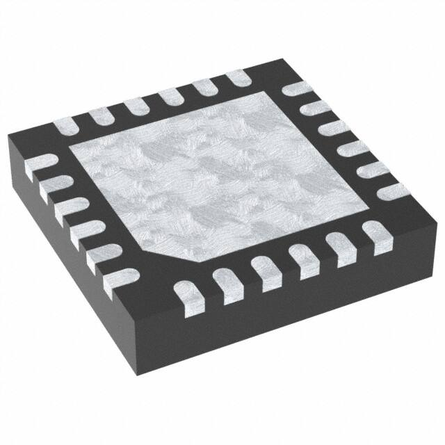


 工商网监
湘ICP备2023018690号
工商网监
湘ICP备2023018690号
