NCV890201
Buck Switching Regulator Automotive
2.0 A, 2 MHz
The NCV890201 is a fixed−frequency, monolithic, Buck switching
regulator intended for Automotive, battery−connected applications
that must operate with up to a 36 V input supply. The regulator is
suitable for systems with low noise and small form factor
requirements often encountered in automotive driver information
systems. The NCV890201 is capable of converting the typical 4.5 V to
18 V automotive input voltage range to outputs as low as 3.3 V at a
constant switching frequency above the sensitive AM band,
eliminating the need for costly filters and EMI countermeasures. Two
pins are provided to synchronize switching to a clock, or to another
NCV890201. The NCV890201 also provides several protection
features expected in Automotive power supply systems such as current
limit, short circuit protection, and thermal shutdown. In addition, the
high switching frequency produces low output voltage ripple even
when using small inductor values and an all−ceramic output filter
capacitor − forming a space−efficient switching regulator solution.
www.onsemi.com
MARKING DIAGRAM
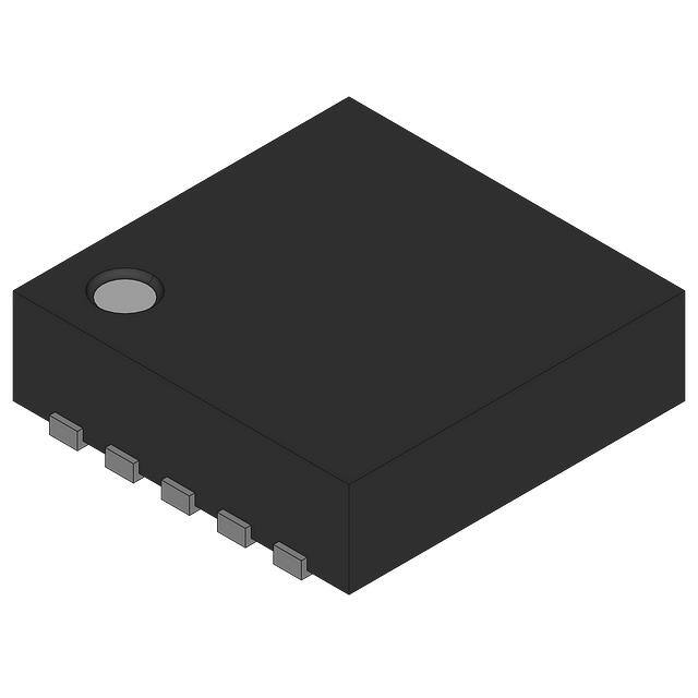
DFN10
CASE 485C
A
= Assembly Location
L
= Wafer Lot
Y
= Year
W
= Work Week
G
= Pb−Free Device
(Note: Microdot may be in either location)
Features
•
•
•
•
•
•
•
•
•
•
•
•
•
ORDERING INFORMATION
Internal N−Channel Power Switch
Low VIN Operation Down to 4.5 V
High VIN Operation to 36 V
Withstands Load Dump to 40 V
2 MHz Free−running Switching Frequency
Auto−synchronizes with Other NCV890201 or to an
External Clock
Logic level Enable Input Can be Directly Tied to
Battery
2.2 A (min) Cycle−by−Cycle Peak Current Limit
Short Circuit Protection enhanced by Frequency
Foldback
±1.75% Output Voltage Tolerance
Output Voltage Adjustable Down to 0.8 V
1.4 Millisecond Internal Soft−Start
Thermal Shutdown (TSD)
CDRV
CIN
SYNC
OUT
EN
1 VIN
2 DRV
4 GND
5 EN
• Low Shutdown Current
• Wettable Flanks DFN
• NCV Prefix for Automotive and Other Applications
•
Requiring Unique Site and Control Change
Requirements; AEC−Q100 Qualified and PPAP
Capable
These Devices are Pb−Free and are RoHS Compliant
Applications
•
•
•
•
L1
SW 10
CBST
DFW
BST 9
3 SYNCO SYNCI 8
See detailed ordering and shipping information in the package
dimensions section on page 18 of this data sheet.
Audio
Infotainment
Safety − Vision Systems
Instrumentation
DBST
NCV890201
VIN
V8902
01
ALYWG
G
SYNC IN
VOUT
COUT
RFB1
FB 7
RFB2
COMP 6
RCOMP
CCOMP
Figure 1. Typical Application
© Semiconductor Components Industries, LLC, 2015
August, 2019 − Rev. 3
1
Publication Order Number:
NCV890201/D
�NCV890201
CDRV
VIN
VIN
CIN
SW
3.3 V
Reg
SYNCO
L1
DFW
CBST
Oscillator
DRV
Sync Out
DBST
PWM
LOGIC
ON OFF
Sync
Out In
BST
SYNCI
Sync In
2A
GND
TSD
Soft−Start
RESET
+
−
+
−
+
+
S
FB
+
COMP
VOLTAGES
MONITORS
Enable
RCOMP
EN
CCOMP
Figure 2. NCV890201 Block Diagram
www.onsemi.com
2
VOUT
COUT
�NCV890201
MAXIMUM RATINGS
Rating
Symbol
Min/Max Voltage VIN
Max Voltage VIN to SW
Min/Max Voltage SW
Min Voltage SW − 20ns
Value
Unit
−0.3 to 40
V
40
V
−0.7 to 40
V
−3.0
V
Min/Max Voltage BST
−0.3 to 40
Min/Max Voltage BST to SW
−0.3 to 3.6
V
Min/Max Voltage on EN
−0.3 to 40
V
Min/Max Voltage COMP
−0.3 to 2
V
Min/Max Voltage FB
−0.3 to 18
V
Min/Max Voltage SYNCO
−0.3 to 3.6
V
Min/Max Voltage DRV
−0.3 to 3.6
V
−0.3 to 6
V
Min/Max Voltage SYNCI
Thermal Resistance, 3x3 DFN Junction−to−Ambient*
50
°C/W
−55 to +150
°C
TJ
−40 to +150
°C
VESD
2.0
200
>1.0
kV
V
kV
MSL
Level 1
RqJA
Storage Temperature range
Operating Junction Temperature Range
ESD withstand Voltage
Human Body Model
Machine Model
Charge Device Model
Moisture Sensitivity
Peak Reflow Soldering Temperature
260
°C
Stresses exceeding those listed in the Maximum Ratings table may damage the device. If any of these limits are exceeded, device functionality
should not be assumed, damage may occur and reliability may be affected.
*Mounted on 1 sq. in. of a 4−layer PCB with 1 oz. copper thickness.
www.onsemi.com
3
�NCV890201
VIN
1
10
SW
DRV
2
9
BST
SYNCO
3
8
SYNCI
GND
4
7
FB
EN
5
6
COMP
(Top View)
Figure 3. Pin Connections
PIN FUNCTION DESCRIPTIONS
Pin No.
Symbol
Description
1
VIN
Input voltage from battery. Place an input filter capacitor in close proximity to this pin.
2
DRV
Output voltage to provide a regulated voltage to the Power Switch gate driver.
3
SYNCO
4
GND
5
EN
6
COMP
Synchronization output. Turn−on of the Power Switch causes the SYNCO signal to fall. SYNCO rises
half a switching period later. Connecting to the SYNCI pin of another NCV890201 causes them to switch
out−of−phase
Battery return, and output voltage ground reference.
This TTL compatible Enable input allows the direct connection of Battery as the enable signal. Grounding
this input stops switching and reduces quiescent current draw to a minimum.
Error Amplifier output, for tailoring transient response with external compensation components.
7
FB
8
SYNCI
9
BST
Bootstrap input provides drive voltage higher than VIN to the N−channel Power Switch for optimum
switch RDS(on) and highest efficiency.
10
SW
Switching node of the Regulator. Connect the output inductor and cathode of the freewheeling diode to
this pin.
Exposed
Pad
Feedback input pin to program output voltage, and detect pre−charged or shorted output conditions.
Synchronization input. Connecting an external clock to the SYNCI pin synchronizes switching to the rising edge of the SYNCI voltage.
Connect to Pin 4 (electrical ground) and to a low thermal resistance path to the ambient temperature
environment.
www.onsemi.com
4
�NCV890201
ELECTRICAL CHARACTERISTICS (VIN = 4.5 V to 28 V, VEN = 5 V, VBST = VSW + 3.0 V, CDRV = 0.1 mF, Min/Max values are valid
for the temperature range −40°C ≤ TJ ≤ 150°C unless noted otherwise, and are guaranteed by test, design or statistical correlation.)
Parameter
Symbol
Conditions
Quiescent Current, shutdown
IqSD
Quiescent Current, enabled
Min
Typ
Max
Unit
VIN = 13.2 V, VEN = 0 V, TJ = 25°C
5
mA
IqEN
VIN = 13.2 V
3
mA
UVLO Start Threshold
VUVLSTT
VIN rising
4.1
4.5
V
UVLO Stop Threshold
VUVLSTP
VIN falling
3.9
4.4
V
UVLO Hysteresis
VUVLOHY
0.1
0.2
V
Logic Low
VENLO
0.8
Logic High
VENHI
QUIESCENT CURRENT
UNDERVOLTAGE LOCKOUT − VIN (UVLO)
ENABLE (EN)
Input Current
IEN
8
tSS
0.8
V
2
V
30
mA
1.4
2.0
ms
0.8
0.814
V
1
mA
SOFT−START (SS)
Soft−Start Completion Time
VOLTAGE REFERENCE
FB Pin Voltage during regulation
VFBR
COMP shorted to FB
0.786
IFBBIAS
VFB = 0.8 V
0.25
gm
VCOMP = 1.3 V
4.5 V < VIN < 18 V
20 V < VIN < 28 V
0.6
0.3
ERROR AMPLIFIER
FB Bias Current
Transconductance
gm(HV)
Output Resistance
COMP Source Current Limit
ROUT
1
0.5
1.5
0.75
1.4
ISOURCE
VFB = 0.63 V, VCOMP = 1.3 V
4.5 V < VIN < 18 V
20 V < VIN < 28 V
75
40
COMP Sink Current Limit
ISINK
VFB = 0.97 V, VCOMP = 1.3 V
4.5 V < VIN < 18 V
20 V < VIN < 28 V
75
40
Minimum COMP voltage
VCMPMIN
VFB = 0.97 V
0.2
FSW
FSW(HV)
4.5 < VIN < 18 V
20 V < VIN < 28 V
1.8
0.9
mmho
MW
mA
mA
0.7
V
2.2
1.1
MHz
OSCILLATOR
Frequency
2.0
1.0
VIN FREQUENCY FOLDBACK MONITOR
Frequency Foldback Threshold
VIN rising
VIN falling
VFLDUP
VFLDDN
Frequency Foldback Hysteresis
VFLDHY
VFB = 0.63 V
18.4
18
0.2
1. Not tested in production. Limits are guaranteed by design.
www.onsemi.com
5
20
19.8
0.3
0.4
V
V
�NCV890201
ELECTRICAL CHARACTERISTICS (VIN = 4.5 V to 28 V, VEN = 5 V, VBST = VSW + 3.0 V, CDRV = 0.1 mF, Min/Max values are valid
for the temperature range −40°C ≤ TJ ≤ 150°C unless noted otherwise, and are guaranteed by test, design or statistical correlation.)
Parameter
Symbol
Conditions
Min
SYNCO Output Pulse Duty Ratio
D(SYNC)
CLOAD = 40 pF
40
SYNCO Output Pulse Falltime
tR(SYNC)
CLOAD = 40 pF, 90% to 10%
SYNCO Output Pulse Risetime
tF(SYNC)
CLOAD = 40 pF, 10% to 90%
SYNCI Input Resistance to ground
RH(SYNC)
VSYNCI = 5.0 V
SYNCI Input High Threshold Voltage
VHSYNC
SYNCI Input Low Threshold Voltage
VLSYNC
SYNCI High Pulse Width
tHSYNCI
SYNCI Low Pulse Width
tLSYNCI
Typ
Max
Unit
60
%
SYNCHRONIZATION
4
ns
4
50
ns
200
k
2.0
V
0.8
V
VSYNC > max VHSYNC
40
ns
VSYNC < min VLSYNC
40
ns
External Sync Frequency
FSYNCI
Master Reassertion Time
tI(SYNC)
Time from last rising SYNCI edge
to first un−synchronized turn−on.
1.8
Sramp
Sramp(HV)
4.5 < VIN < 18 V
20 V < VIN < 28 V
ON Resistance
RDSON
Leakage current VIN to SW
2.5
650
MHz
ns
SLOPE COMPENSATION
1.3
0.6
A/ms
VBST = VSW + 3.0 V
650
mW
ILKSW
VEN = 0 V, VSW = 0, VIN = 18 V
10
mA
Minimum ON Time
tONMIN
Measured at SW pin
70
ns
Minimum OFF Time
tOFFMIN
Measured at SW pin
At FSW = 2 MHz (normal)
At FSW = 500 kHz (max duty cycle)
Ramp Slope (Note 1)
(With respect to switch current)
0.7
0.25
POWER SWITCH
45
ns
30
30
50
70
2.2
2.45
2.7
A
400
200
24
500
250
32
600
300
40
kHz
VDRV
3.1
3.3
3.5
V
DRV POR Start Threshold
VDRVSTT
2.7
2.9
3.05
V
DRV POR Stop Threshold
VDRVSTP
2.5
2.8
3.0
V
45
mA
50
mV
PEAK CURRENT LIMIT
Current Limit Threshold
ILIM
SHORT CIRCUIT FREQUENCY FOLDBACK
Lowest Foldback Frequency
Lowest Foldback Frequency − High Vin
Hiccup Mode
FSWAF
FSWAFHV
FSWHIC
VFB = 0 V, 4.5 V < VIN < 18 V
VFB = 0 V, 20 V < VIN < 28 V
VFB = 0 V
GATE VOLTAGE SUPPLY (DRV pin)
Output Voltage
DRV Current Limit
IDRVLIM
VDRV = 0 V
16
OUTPUT PRECHARGE DETECTOR
VSSEN
20
Activation Temperature (Note 1)
TSD
150
190
°C
Hysteresis (Note 1)
THYS
5
20
°C
Threshold Voltage
35
THERMAL SHUTDOWN
1. Not tested in production. Limits are guaranteed by design.
Product parametric performance is indicated in the Electrical Characteristics for the listed test conditions, unless otherwise noted. Product
performance may not be indicated by the Electrical Characteristics if operated under different conditions.
www.onsemi.com
6
�NCV890201
VIN = 13.2 V
7
6
5
4
3
2
1
0
−50
−25
0
25
50
75
100
125
IqEN. ENABLED QUIESCENT CURRENT
(mA)
8
150
2.4
2.2
2.0
1.8
1.6
1.4
1.2
1.0
−50
25
50
75
100
125
Figure 5. Enabled Quiescent Current vs.
Junction Temperature
4.5
4.4
4.3
4.2
4.1
4.0
−25
0
25
50
75
100
125
TJ. JUNCTION TEMPERATURE (°C)
150
4.5
4.4
4.3
4.2
4.1
4.0
3.9
3.8
3.7
−50
−25
VFBR. FB REGULATION VOLTAGE (V)
2.2
2.0
1.8
1.6
1.4
1.2
1.0
0.8
0
25
50
75
100
125
0
25
50
75
100
125
TJ. JUNCTION TEMPERATURE (°C)
150
Figure 7. UVLO Stop Threshold vs. Junction
Temperature
2.4
−25
150
4.6
Figure 6. UVLO Start Threshold vs. Junction
Temperature
tSS. SOFT−START DURATION (ms)
0
Figure 4. Shutdown Quiescent Current vs.
Junction Temperature
4.6
0.6
−50
−25
TJ. JUNCTION TEMPERATURE (°C)
4.7
3.9
−50
2.6
TJ. JUNCTION TEMPERATURE (°C)
VUVLSTP. UVLO STOP THRESHOLD (V)
VUVLSTT. UVLO START THRESHOLD (V)
IqSD. SHUTDOWN QUIESCENT CURRENT
(mA)
TYPICAL CHARACTERISTICS CURVES
150
0.85
0.84
0.83
0.82
0.81
0.80
0.79
0.78
0.77
0.76
0.75
−50
−25
0
25
50
75
100
125
TJ. JUNCTION TEMPERATURE (°C)
TJ. JUNCTION TEMPERATURE (°C)
Figure 8. Soft−Start Duration vs. Junction
Temperature
Figure 9. FB Regulation Voltage vs. Junction
Temperature
www.onsemi.com
7
150
�NCV890201
TYPICAL CHARACTERISTICS CURVES
100
1.2
1.0
VIN = 4.5 V
0.8
0.6
VIN = 28 V
0.4
0.2
−50
−25
0
25
50
75
100
125
70
60
50
VIN = 28 V
40
30
20
−50
−25
0
25
50
75
100
125
TJ. JUNCTION TEMPERATURE (°C)
TJ. JUNCTION TEMPERATURE (°C)
Figure 10. Error Amplifier Transconductance
vs. Junction Temperature
Figure 11. Error Amplifier Max Sourcing
Current vs. Junction Temperature
FSW. OSCILLATOR FREQENCY (MHz)
90
VIN = 4.5 V
80
70
60
50
VIN = 28 V
40
30
20
−50
−25
0
25
50
75
100
125
150
VIN = 13.2 V
2.0
1.8
1.6
1.4
1.2
VIN = 28 V
1.0
0.8
−50
−25
0
25
50
75
100
125
TJ. JUNCTION TEMPERATURE (°C)
TJ. JUNCTION TEMPERATURE (°C)
Figure 12. Error Amplifier Max Sinking Current
vs. Junction Temperature
Figure 13. Oscillator Frequency vs. Junction
Temperature
19.6
56
19.4
55
19.2
VFLDUP
19.0
VFLDDN
18.8
18.6
18.4
18.2
−50
−25
0
25
50
75
100
125
TJ. JUNCTION TEMPERATURE (°C)
150
150
54
53
52
51
50
49
48
−50
Figure 14. Rising Frequency Foldback
Threshold vs. Junction Temperature
−25
0
25
50
75
100
125
TJ. JUNCTION TEMPERATURE (°C)
Figure 15. SYNCO Pulse Duty Ratio vs.
Junction Temperature
www.onsemi.com
8
150
2.2
D(SYNC). SYNCO PULSE DUTY
RATIO (%)
ISINK. ERROR AMPLIFIER SINKING
CURRENT (mA)
VIN = 4.5 V
80
150
100
VFLDUP. VFLDDN, FREQ. FOLDBACK
THRESHOLD (V)
90
ISOURCE. ERROR AMPLIFIER
SOURCING CURRENT (mA)
gm. ERROR AMPLIFIER
TRANSCONDUCTANCE (mS)
1.4
150
�NCV890201
TYPICAL CHARACTERISTICS CURVES
900
RDS(on). POWER SWITCH ON
RESISTANCE (mW)
RH(SYNC). SYNCI INPUT
RESISTANCE (kW)
160
140
120
100
80
60
40
−50
−25
0
25
50
75
100
125
800
700
600
500
400
300
200
100
0
−50
150
−25
TJ. JUNCTION TEMPERATURE (°C)
80
75
75
70
70
65
60
55
50
45
40
−50
−25
0
25
50
75
100
125
150
60
55
50
45
40
35
−50
−25
0
25
50
75
100
125
TJ. JUNCTION TEMPERATURE (°C)
Figure 18. Minimum On Time vs. Junction
Temperature
Figure 19. Minimum Off Time vs. Junction
Temperature
150
600
2.80
FSWAF. FOLDBACK MODE
SWITCHING FREQUENCY (kHz)
ILIM, PEAK CURRENT LIMIT (A)
65
TJ. JUNCTION TEMPERATURE (°C)
2.90
2.70
2.60
2.50
2.40
2.30
2.20
2.10
2.00
−50
15 0
Figure 17. Power Switch RDS(on) vs. Junction
Temperature
tOFFMIN. MINIMUM TIME (ns)
tONMIN. MINIMUM TIME (ns)
Figure 16. SYNCI Input Resistance vs.
Junction Temperature
0
25
50
75
100
125
TJ. JUNCTION TEMPERATURE (°C)
−25
0
25
50
75
100
125
150
VIN = 4.5 V
550
500
450
400
350
300
VIN = 28 V
250
200
−50
−25
0
25
50
75
100
125
150
TJ. JUNCTION TEMPERATURE (°C)
TJ. JUNCTION TEMPERATURE (°C)
Figure 20. Current Limit Threshold vs.
Junction Temperature
Figure 21. Short−Circuit Foldback Frequency
vs. Junction Temperature
www.onsemi.com
9
�NCV890201
40
3.50
38
3.45
VDRV. DRV VOLTAGE (V)
FSWHC. HICCUP MODE FREUQNCY
(kHz)
TYPICAL CHARACTERISTICS CURVES
36
34
32
30
28
3.35
IDRV = 0 mA
3.30
IDRV = 16 mA
3.25
3.20
3.15
26
24
−50
−25
0
25
50
75
100
125
3.10
−50
150
−25
0
25
50
75
100
125
TJ. JUNCTION TEMPERATURE (°C)
TJ. JUNCTION TEMPERATURE (°C)
Figure 22. Hiccup Mode Switching Frequency
vs. Junction Temperature
Figure 23. DRV Voltage vs. Junction
Temperature
3.1
150
IDRVLIM. DRV CURRENT LIMIT (mA)
30
3.0
2.9
VDRVSTT
2.8
VDRVSTP
2.7
2.6
2.5
−50
−25
0
25
50
75
100
125
TJ. JUNCTION TEMPERATURE (°C)
150
29
28
27
26
25
24
23
22
21
−50
Figure 24. DRV Reset Threshold vs. Junction
Temperature
−25
0
25
50
75
100
125
TJ. JUNCTION TEMPERATURE (°C)
Figure 25. DRV Current Limit vs. Junction
Temperature
55
VSSEN. OUTPUT PRECHARGE
DETECTOR THRESHOLD (V)
VDRVSTT. VDRVSTP, DRV RESET
THRESHOLDS (V)
3.40
50
45
40
35
30
25
20
−50
−25
0
25
50
75
100
125
TJ. JUNCTION TEMPERATURE (°C)
Figure 26. Output Precharge Detector
Threshold vs. Junction Temperature
www.onsemi.com
10
150
150
�NCV890201
GENERAL INFORMATION
INPUT VOLTAGE
SLOPE COMPENSATION
An Undervoltage Lockout (UVLO) circuit monitors the
input, and inhibits switching and resets the Soft−start circuit
if there is insufficient voltage for proper regulation. The
NCV890201 can regulate a 3.3 V output with input voltages
above 4.5 V and a 5.0 V output with an input above 6.5 V.
The NCV890201 withstands input voltages up to 40 V.
To limit the power lost in generating the drive voltage for
the Power Switch, the switching frequency is reduced by a
factor of 2 when the input voltage exceeds the VIN
Frequency Foldback threshold VFLDUP (see Figure 27).
Frequency reduction is automatically terminated when the
input voltage drops back below the VIN Frequency Foldback
threshold VFLDDN.
A fixed slope compensation signal is generated internally
and added to the sensed current to avoid increased output
voltage ripple due to bifurcation of inductor ripple current
at duty cycles above 50%. The fixed amplitude of the slope
compensation signal requires the inductor to be greater than
a minimum value, depending on output voltage, in order to
avoid sub−harmonic oscillations. For 3.3 V and 5 V output
voltages, the recommended inductor value is 4.7 mH.
SHORT CIRCUIT FREQUENCY FOLDBACK
During severe output overloads or short circuits, the
NCV890201 automatically reduces its switching frequency.
This creates duty cycles small enough to limit the peak
current in the power components, while maintaining the
ability to automatically reestablish the output voltage if the
overload is removed. If the current is still too high after the
switching frequency folds back to 500 kHz, the regulator
enters an auto−recovery burst mode that further reduces the
dissipated power.
Fsw
(MHz)
2
CURRENT LIMITING
Due to the ripple on the inductor current, the average
output current of a buck converter is lower than the peak
current setpoint of the regulator. Figure 28 shows − for a
4.7 mH inductor − how the variation of inductor peak current
with input voltage affects the maximum DC current the
NCV890201 can deliver to a load.
1
4
18 20
36
VIN (V)
2.3
MINIMUM CURRENT LIMIT (A)
Figure 27. NCV890201 Switching Frequency
Reduction at High Input Voltage
ENABLE
The NCV890201 is designed to accept either a logic level
signal or battery voltage as an Enable signal. EN low induces
a ’sleep mode’ which shuts off the regulator and minimizes
its supply current to a couple of mA typically (IqSD) by
disabling all functions. Upon enabling, voltage is
established at the DRV pin, followed by a soft−start of the
switching regulator output.
2.2
(3.3 VOUT)
2.1
(5 VOUT)
2.0
1.9
1.8
1.7
1.6
0
5
SOFT−START
10
15
20
25
30
35
40
INPUT VOLTAGE (V)
Upon being enabled or released from a fault condition,
and after the DRV voltage is established, a soft−start circuit
ramps the switching regulator error amplifier reference
voltage to the final value. During soft−start, the average
switching frequency is lower than its normal mode value
(typically 2 MHz) until the output voltage approaches
regulation.
Figure 28. NCV890201 Load Current Capability
with 4.7 mH Inductor
www.onsemi.com
11
�NCV890201
SYNCHRONIZATION
does not arrive at the SYNCI pin within the Master
Reassertion Time, the NCV890201 controls its own
switching frequency, allowing uninterrupted operation in
the event that the clock (or controlling NCV890201) is
turned off.
If internal conditions or excessive input voltage cause an
NCV890201 to fold back its switching frequency, the main
oscillator switching frequency is no longer derived from the
frequency received at the SYNCI pin. Under these
conditions, the SYNCO pin is held low.
An external pulldown resistor is not required at the
SYNCI pin if it is unconnected.
Two NCV890201 can be synchronized out−of−phase to
one another by connecting the SYNCO pin of one to the
SYNCI pin of the other (Figure 29). Any number of
NCV890201 can also be synchronized to an external clock
(Figure 30). If a part does not have its switching frequency
controlled by the SYNCI input, it drives the SYNCO pin low
when it turns on the power switch, and drives it high half a
switching period later. When the switching frequency is
controlled by the SYNCI input, the SYNCO pin is held low.
Synchronization starts within 2 ms of soft−start completion.
A rising edge at the SYNCI pin causes an NCV890201 to
immediately turn on the power switch. If another rising edge
VIN
CDRV1
CDRV2
DBST2
NCV890201
1 VIN
CIN2
2 DRV
3 SYNCO
4 GND
EN2
L2
SW 10
DBST1
NCV890201
CBST2
BST 9
DFW2
RFB1
SYNCI 8
CIN1
VOUT2
1 VIN
SW 10
CBST
1
2 DRV
COUT2
3 SYNCO
BST 9
FB 7
RFB1
FB 7
COMP 6
5 EN
VOUT1
COUT1
DFW1
SYNCI 8
4 GND
Synchronization
L1
RFB2
RCOMP1
5 EN
RFB2
COMP 6
SYNC MASTER
CCOMP1
RCOMP2
SYNC SLAVE
CCOMP2
Figure 29. NCV890201s Synchronized to Each Other
Master Enabled by Battery
VIN
CDRV1
DBST2
NCV890201
1 VIN
CIN2
2 DRV
3 SYNCO
4 GND
EN2
SW 10
BST 9
DBST1
NCV890201
CDRV
2
L2
CIN1
VOUT2
2 DRV
CBST2
DFW2RFB21
1 VIN
COUT2
3 SYNCO
SYNCI 8
4 GND
FB 7
BST 9
SYNCI 8
DFW1
RFB11
FB 7
COMP 6
5 EN
L1
SW 10
CBST
1
RFB12
RCOMP1
5 EN
COMP 6
RFB22
CCOMP1
RCOMP2
Synchronization
CCOMP2
CLK
Figure 30. Both NCV890201s Synchronized to External Clock
#1 Enabled by Battery
www.onsemi.com
12
VOUT1
COUT1
�NCV890201
BOOTSTRAP
In order for the bootstrap capacitor to stay charged, the
Switch node needs to be pulled down to ground regularly. In
very light load condition, the NCV890201 skips switching
cycles to ensure the output voltage stays regulated. When the
skip cycle repetition frequency gets too low, the bootstrap
voltage collapses and the regulator stops switching.
Practically, this means that the NCV890201 needs a
minimum load to operate correctly. Figure 31 shows the
minimum current requirements for different input and
output voltages.
At the DRV pin an internal regulator provides a
ground−referenced voltage to an external capacitor (CDRV),
to allow fast recharge of the external bootstrap capacitor
(CBST) used to supply power to the power switch gate driver.
If the voltage at the DRV pin goes below the DRV UVLO
Threshold VDRVSTP, switching is inhibited and the
Soft−start circuit is reset, until the DRV pin voltage goes
back up above VDRVSTT.
16
MINIMUM OUTPUT CURRENT (mA)
MINIMUM OUTPUT CURRENT (mA)
50
40
L = 2.2 mH
30
20
L = 4.7 mH
10
0
4.2
5.2
6.2
7.2
8.2
9.2
8
6
4
L = 2.2 mH
2
0
4.2
4.7
5.2
5.7
6.2
Minimum Load 5 V Out
Minimum Load 3.3 V Out
6.7
50
MINIMUM OUTPUT CURRENT (mA)
MINIMUM OUTPUT CURRENT (mA)
L = 4.7 mH
10
INPUT VOLTAGE (V)
18
16
14
12
10
L = 2.2 mH
8
L = 4.7 mH
4
2
0
12
INPUT VOLTAGE (V)
20
6
14
4.2
4.7
5.2
5.7
6.2
6.7
7.2
45
40
L = 2.2 mH
35
30
25
20
L = 4.7 mH
15
10
5
0
4.2
6.2
8.2
INPUT VOLTAGE (V)
INPUT VOLTAGE (V)
Minimum Load 3.7 V Out
Minimum Load 5.5 V Out
Figure 31. Minimum Load Current with Different Input and Output Voltages
www.onsemi.com
13
10.2
7.2
�NCV890201
OUTPUT PRECHARGE DETECTION
EXPOSED PAD
Prior to Soft−start, the FB pin is monitored to ensure the
SW voltage is low enough to have charged the external
bootstrap capacitor (CBST). If the FB pin is higher than
VSSEN, restart is delayed until the output has discharged.
The exposed pad (EPAD) on the back of the package must
be electrically connected to the electrical ground (GND pin)
for proper, noise−free operation.
DESIGN METHODOLOGY
The NCV890201 being a fixed−frequency regulator with
the switching element integrated, is optimized for one value
of inductor. This value is set to 4.7 mH, and the slope
compensation is adjusted for this inductor. The only
components left to be designed are the input and output
capacitor and the freewheeling diode. Please refer to the
design spreadsheet www.onsemi.com NCV890201 page
that helps with the calculation.
Output capacitor:
The minimum output capacitor value can be calculated
based on the specification for output voltage ripple:
THERMAL SHUTDOWN
A thermal shutdown circuit inhibits switching, resets the
Soft−start circuit, and removes DRV voltage if internal
temperature exceeds a safe level. Switching is automatically
restored when temperature returns to a safe level. Figure 32
shows the IC starts to switch after the voltage on FB pin
reaches VSSEN, even the EN pin is high. After the IC is
switching, the FB pin follows the soft starts reference to
reach the final set point.
EN
C OUT min +
DI L
8 @ DV OUT @ F SW
With
Time
− DIL the inductor ripple current:
FB
ǒ
V OUT @ 1 *
VSSEN
DI L +
Time
V
Ǔ
OUT
V
IN
(eq. 2)
L @ F SW
− DVOUT the desired voltage ripple.
However, the ESR of the output capacitor also contributes
to the output voltage ripple, so to comply with the
requirement, the ESR cannot exceed RESRmax:
SW
Figure 32. Output Voltage Detection
(eq. 1)
R ESR max +
Time
DV OUT @ L @ F SW
ǒ
V OUT 1 *
V
Ǔ
OUT
V
IN
(eq. 3)
Finally, the output capacitor must be able to sustain the ac
current (or RMS ripple current):
MINIMUM DROPOUT VOLTAGE
When operating at low input voltages, two parameters
play a major role in imposing a minimum voltage drop
across the regulator: the minimum off time (that sets the
maximum duty cycle), and the on state resistance.
When operating in continuous conduction mode (CCM),
the output voltage is equal to the input voltage multiplied by
the duty ratio. Because the NCV890201 needs a sufficient
bootstrap voltage to operate, its duty cycle cannot be 100%:
it needs a minimum off time (tOFFmin) to periodically re−fuel
the bootstrap capacitor CBST. This imposes a maximum duty
ratio DMAX = 1 − tOFFmin.FSW(min), with the switching
frequency being folded back down to FSW(min) = 500 kHz to
keep regulating at the lowest input voltage possible.
The drop due to the on−state resistance is simply the
voltage drop across the Switch resistance RDSON at the
given output current: VSWdrop = IOUT.RDSon.
Which leads to the maximum output voltage in low Vin
condition: VOUT = DMAX.VIN(min) − VSWdrop
I OUTac +
DI L
2 Ǹ3
(eq. 4)
Typically, with the recommended 4.7 mH inductor, two
ceramic capacitors of 10 mF each in parallel give very good
results.
Freewheeling diode:
The diode must be chosen according to its maximum
current and voltage ratings, and to thermal considerations.
As far as max ratings are concerned, the maximum reverse
voltage the diode sees is the maximum input voltage (with
some margin in case of ringing on the Switch node), and the
maximum forward current the peak current limit of the
NCV890201, ILIM.
The power dissipated in the diode is PDloss:
ǒ
P Dloss + I OUT @ 1 *
www.onsemi.com
14
Ǔ
V OUT
V IN
@ V F ) I DRMS @ R D (eq. 5)
�NCV890201
with:
− IOUT the average (dc) output current
− VF the forward voltage of the diode
− IDRMS the RMS current in the diode:
I DRMS +
Ǹ
ǒ
(1 * D) I OUT 2 )
DI L
12
Ǔ
It can be designed in combination with an inductor to build
an input filter to filter out the ripple current in the source, in
order to reduce EMI conducted emissions.
For example, using a 4.7 mH input capacitor, it is easy to
calculate that an inductor of 200 nH will ensure that the
input filter has a cut−off frequency below 200 kHz (low
enough to attenuate the 2 MHz ripple).
2
(eq. 6)
− RD the dynamic resistance of the diode (extracted from
the V/I curve of the diode in its datasheet).
Then, knowing the thermal resistance of the package and
the amount of heatsinking on the PCB, the temperature rise
corresponding to this power dissipation can be estimated.
Error Amplifier and Loop Transfer Function
The error amplifier is a transconductance type amplifier.
The output voltage of the error amplifier controls the peak
inductor current at which the power switch shuts off. The
Current Mode control method employed allows the use of a
simple, type II compensation to optimize the dynamic
response according to system requirements.
Figure 33 shows the error amplifier with the
compensation components and the voltage feedback divider.
Input capacitor:
The input capacitor must sustain the RMS input ripple
current IINac:
I INac +
DI L
VOUT
2
ǸD3
(eq. 7)
RFB1
VCOMP
VFB
V
RCOMP
RFB2
Cp
gm * V
RO
CCOMP
Vref
Figure 33. Feedback Compensator Network Model
The transfer function from VOUT to VCOMP is the
product of the feedback voltage divider and the error
amplifier.
RFB2
RFB1 ) RFB2
s
1 ) wz
Gerr amp(s) + gm @ Ro @
1) s
1) s
wpl
wph
Gdivider(s) +
ǒ
Ǔǒ
Ǔ
1
RCOMP @ CCOMP
1
wpl +
Ro @ CCOMP
wz +
(eq. 8)
wph +
(eq. 9)
(eq. 10)
(eq. 11)
1
RCOMP @ Cp
(eq. 12)
The output resistor Ro of the error amplifier is 1.4 MW and
gm is 1 mA/V. The capacitor Cp is for rejecting noise at high
frequency and is integrated inside the IC with a value of
18 pF.
The power stage transfer function (from Vcomp to output)
is shown below:
s
1 ) wz
1
Gps(s) + Rload @
@
@ Fh(s) (eq. 13)
Ri
s
1 ) Rload@Tsw @ [Mc @ (1 * D) * 0.5]
1
)
L
wp
ǒ
www.onsemi.com
15
Ǔ
wz +
1
Resr @ Cout
wp +
Mc @ (1 * D) * 0.5
1
(eq. 15)
)
L @ Cout @ Fsw
Rload @ Cout
(eq. 14)
�NCV890201
where
Mc + 1 ) Se
Sn
Vin
*
Vout @ Ri
Sn +
L
The bode plots of the open loop transfer function will
show the gain and phase margin of the system. The
compensation network is designed to make sure the system
has enough phase margin and bandwidth.
(eq. 16)
(eq. 17)
Ri represents the equivalent sensing resistor which has a
value of 0.183 W, Se is the compensation slope which is
183 kV/S, Sn is the slope of the sensing resistor current
during on time. Fh(s) represents the sampling effect from the
current loop which has two poles at one half of the switching
frequency:
1
2
s
) s
wn@Qp wn 2
wn + p @ Fsw
Fh(s) +
Qp +
Design of the Compensation Network
The function of the compensation network is to provide
enough phase margin at crossover frequency to stabilize the
system as well as to provide high gain at low frequency to
eliminate the steady state error of the output voltage. Please
refer to the design spreadsheet www.onsemi.com
NCV890201 page that helps with the calculation.
The design steps will be introduced through an example.
Example:
Vin = 15.5 V, Vout = 3.3 V, Rload = 1.65 W, Iout = 2 A, L =
4.7 mH, Cout = 20 mF (Resr = 7 mW)
The reference voltage of the feedback signal is 0.8 V and
to meet the minimum load requirements, select RFB1 =
100 W, RFB2 = 31.6 W.
From the specification, the power stage transfer function can
be plotted as below:
(eq. 18)
1)
1
p @ [Mc @ (1 * D) * 0.5]
(eq. 19)
The total loop transfer function is the product of power
stage and feedback compensation network.
(dB)
Gloop(s) + Gdivider(s) @ Gerr amp(s) @ Gps(s) (eq. 20)
20 x log
⎣
Gps ⎣f ( m)⎦
⎦
90
180
45
90
0
0
− 45
− 90
100
arg (Gps (f m)) x
180
p
− 90
3
4
1⋅ 10
− 180
6
1⋅ 10
5
1⋅ 10
fm
1⋅ 10
(Hz)
Figure 34. Power Stage Bode Plots
The crossover frequency is chosen to be Fc = 70 kHz, the
power stage gain at this frequency is −4 dB (0.634) from
calculation. Then the gain of the feedback compensation
network must be 4 dB. Next is to decide the locations of one
zero and one pole of the compensator. The zero is to provide
phase boost at the crossover frequency and the pole is to
reject the noise of high frequency. In this example, a zero is
placed at 1/10 of the crossover frequency and a pole is placed
at 1/5 of the switching frequency (Fsw = 2 MHz):
Fz = 7000 Hz, Fp = 400000 Hz,
RCOMP, CCOMP and Cp can be calculated from the
following equations:
RCOMP +
Fp @ gm
@ Vout @
(Fp * Fz) @ |Gps(Fc)| Vref
CCOMP +
Cp +
Ǹ
ǒ Ǔ
1 ) Fc
Fp
Ǹ
1
2p @ Fz @ RCOMP
1
2p @ Fp @ RCOMP
(eq. 21)
ǒ Ǔ
1 ) Fz
Fc
2
2
(eq. 22)
(eq. 23)
Note: there is an 18 pF capacitor at the output of the OTA
integrated in the IC, and if a larger capacitor needs to be
used, subtract this value from the calculated Cp. Figure 35
shows Cp is split into two capacitors. Cint is the 18 pF in the
IC. Cext is the extra capacitor added outside the IC.
www.onsemi.com
16
�NCV890201
From the calculation:
RCOMP = 6.6 KW, CCOMP = 3.4 nF, Cp = 48 pF
So the feedback compensation network is as below:
VOUT
RFB1
100 W
VCOMP
VFB
V
RFB2
31.6 W
gm*V
Vref
0.8 V
RCOMP
6.6 KW
18 pF
Cint
RO
CCOMP
30 pF
Cext
3.4 nF
Figure 35. Example of the Feedback Compensation Network
(dB)
Figure 36 shows the bode plot of the OTA compensator
20 x log
⎣
Gerr_amp ⎣f ( m )⎦
⎦
90
180
45
90
0
0
− 45
− 90
100
arg (Gerr_amp (f m )) x
180
p
− 90
1 ⋅ 10
3
1 ⋅ 10
4
1 ⋅ 10
− 180
6
1 ⋅ 10
5
fm
(Hz)
Figure 36. Bode Plot of the OTA Compensator
(dB)
The total loop bode plot is as below:
20 x log ⎣ Gloop ⎣f ( m )⎦
90
180
45
90
arg(Gloop (f m ))‧
⎦ 0
0
− 45
− 90
− 90
100
3
1⋅ 10
4
1⋅ 10
fm
(Hz)
Figure 37. Bode Plot of the Total Loop
The crossover frequency is at 70 KHz and phase margin is 75 degrees.
www.onsemi.com
17
5
1⋅ 10
− 180
6
1⋅ 10
180
p
�NCV890201
Freewheeling diode ³ inductor ³ Output capacitor
³ return through ground
− Minimize the length of high impedance signals, and
route them far away from the power loops:
♦ Feedback trace
♦ Comp trace
PCB LAYOUT RECOMMENDATION
♦
As with any switching power supplies, there are some
guidelines to follow to optimize the layout of the printed
circuit board for the NCV890201. However, because of the
high switching frequency extra care has to be taken.
− Minimize the area of the power current loops:
♦ Input capacitor ³ NCV890201 switch ³ Inductor
³ output capacitor ³ return through Ground
ORDERING INFORMATION
Device
NCV890201MWTXG
Package
Shipping†
DFN10 with wettable flanks
(Pb−Free)
3000 / Tape & Reel
†For information on tape and reel specifications, including part orientation and tape sizes, please refer to our Tape and Reel Packaging
Specifications Brochure, BRD8011/D.
www.onsemi.com
18
�MECHANICAL CASE OUTLINE
PACKAGE DIMENSIONS
DFN10, 3x3, 0.5P
CASE 485C
ISSUE F
SCALE 2:1
DATE 16 DEC 2021
GENERIC
MARKING DIAGRAM*
XXXXX
XXXXX
ALYWG
G
XXXXX = Specific Device Code
A
= Assembly Location
L
= Wafer Lot
*This information is generic. Please refer to
Y
= Year
device data sheet for actual part marking.
W
= Work Week
Pb−Free indicator, “G” or microdot “G”, may
G
= Pb−Free Package
or may not be present. Some products may
(Note: Microdot may be in either location) not follow the Generic Marking.
DOCUMENT NUMBER:
DESCRIPTION:
98AON03161D
Electronic versions are uncontrolled except when accessed directly from the Document Repository.
Printed versions are uncontrolled except when stamped “CONTROLLED COPY” in red.
DFN10, 3X3 MM, 0.5 MM PITCH
PAGE 1 OF 1
onsemi and
are trademarks of Semiconductor Components Industries, LLC dba onsemi or its subsidiaries in the United States and/or other countries. onsemi reserves
the right to make changes without further notice to any products herein. onsemi makes no warranty, representation or guarantee regarding the suitability of its products for any particular
purpose, nor does onsemi assume any liability arising out of the application or use of any product or circuit, and specifically disclaims any and all liability, including without limitation
special, consequential or incidental damages. onsemi does not convey any license under its patent rights nor the rights of others.
© Semiconductor Components Industries, LLC, 2019
www.onsemi.com
�onsemi,
, and other names, marks, and brands are registered and/or common law trademarks of Semiconductor Components Industries, LLC dba “onsemi” or its affiliates
and/or subsidiaries in the United States and/or other countries. onsemi owns the rights to a number of patents, trademarks, copyrights, trade secrets, and other intellectual property.
A listing of onsemi’s product/patent coverage may be accessed at www.onsemi.com/site/pdf/Patent−Marking.pdf. onsemi reserves the right to make changes at any time to any
products or information herein, without notice. The information herein is provided “as−is” and onsemi makes no warranty, representation or guarantee regarding the accuracy of the
information, product features, availability, functionality, or suitability of its products for any particular purpose, nor does onsemi assume any liability arising out of the application or use
of any product or circuit, and specifically disclaims any and all liability, including without limitation special, consequential or incidental damages. Buyer is responsible for its products
and applications using onsemi products, including compliance with all laws, regulations and safety requirements or standards, regardless of any support or applications information
provided by onsemi. “Typical” parameters which may be provided in onsemi data sheets and/or specifications can and do vary in different applications and actual performance may
vary over time. All operating parameters, including “Typicals” must be validated for each customer application by customer’s technical experts. onsemi does not convey any license
under any of its intellectual property rights nor the rights of others. onsemi products are not designed, intended, or authorized for use as a critical component in life support systems
or any FDA Class 3 medical devices or medical devices with a same or similar classification in a foreign jurisdiction or any devices intended for implantation in the human body. Should
Buyer purchase or use onsemi products for any such unintended or unauthorized application, Buyer shall indemnify and hold onsemi and its officers, employees, subsidiaries, affiliates,
and distributors harmless against all claims, costs, damages, and expenses, and reasonable attorney fees arising out of, directly or indirectly, any claim of personal injury or death
associated with such unintended or unauthorized use, even if such claim alleges that onsemi was negligent regarding the design or manufacture of the part. onsemi is an Equal
Opportunity/Affirmative Action Employer. This literature is subject to all applicable copyright laws and is not for resale in any manner.
PUBLICATION ORDERING INFORMATION
LITERATURE FULFILLMENT:
Email Requests to: orderlit@onsemi.com
onsemi Website: www.onsemi.com
◊
TECHNICAL SUPPORT
North American Technical Support:
Voice Mail: 1 800−282−9855 Toll Free USA/Canada
Phone: 011 421 33 790 2910
Europe, Middle East and Africa Technical Support:
Phone: 00421 33 790 2910
For additional information, please contact your local Sales Representative
�


 工商网监
湘ICP备2023018690号
工商网监
湘ICP备2023018690号
