NCV891234, NCV891334
2 MHz Low-IQ Dual-Mode
Step-Down Regulator for
Automotive
The NCV891x34 is a Dual Mode regulator intended for Automotive,
battery−connected applications that must operate with up to a 45 V
input supply. Hybrid Low Power Mode allows the NCV891x34 to
operate either as a PWM Buck Converter or as a Low Drop−Out Linear
Regulator, and the NCV891x34 is suitable for systems with Low Noise
and Low Quiescent Current requirements often encountered in
automotive driver information systems. A reset (with fixed delay) and
a fault pin (flagging low input voltage and high temperature warnings)
simplify interfacing with a microcontroller.
Two pins are provided to synchronize switching to a clock, or to
another NCV891x34. The NCV891x34 also provides several protection
features expected in automotive power supply systems such as current
limit, short circuit protection, and thermal shutdown. In addition, the
high switching frequency produces low output voltage ripple even
when using small inductor values and an all−ceramic output filter
capacitor – forming a space−efficient switching regulator solution.
www.onsemi.com
1
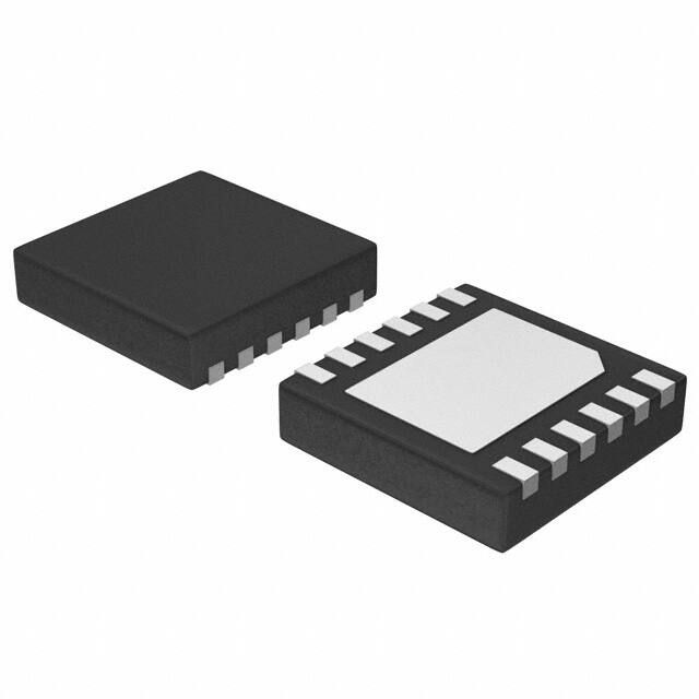
DFN12
MW SUFFIX
CASE 506CE
MARKING DIAGRAM
891x34
XX
ALYWG
G
Features
•
•
•
•
•
•
•
•
•
•
•
•
40 mA Iq in Light Load Condition
2.0 A Maximum Output Current in PWM Mode in NCV891234
3.0 A Maximum Output Current in PWM Mode in NCV891334
Internal N−channel Power Switch
VIN Operating Range 3.7 V to 36 V, Withstands Load Dump to 45 V
Logic Level Enable Pin can be Tied to Battery
Fixed Output Voltage of 5.0 V or 3.3 V with ±2% Accuracy
2 MHz Free−running Switching Frequency
Input and Output Synchronization Pins
NCV Prefix for Automotive Requiring Site and Control Changes
Wettable Flanks DFN (pin edge plating)
These Devices are Pb−Free and are RoHS Compliant
Typical Applications
•
•
•
•
Safety−Vision Systems
Audio, Infotainment
Instrumentation
Telematics
891x34XX = Specific Device Code
x
= 2, 3
XX
= 33, 50
A
= Assembly Location
L
= Wafer Lot
Y
= Year
W
= Work Week
G
= Pb−Free Device
(Note: Microdot may be in either location)
PIN CONNECTIONS
VIN
1
SW
VIN2
BST
DRV
VOUT
SYNCO
EN
RSTB
SYNCI
GND
CDRV
FLTB
DBST
VIN
VIN
NCV891x34
SW
L1
VOUT
(Top View)
CBST
CIN
VIN2
BST
DRV
VOUT
DFW
COUT
ORDERING INFORMATION
See detailed ordering and shipping information on page 10 of
this data sheet.
SYNCO
SYNCO
EN
RESET
ENABLE
RSTB
SYNCI
SYNCI
GND
FLTB
FAULT
Figure 1. Application Schematic
© Semiconductor Components Industries, LLC, 2016
June, 2016 − Rev. 0
1
Publication Order Number:
NCV891334/D
�NCV891234, NCV891334
CDRV
VIN
CIN
DBST
SW
VIN
L1
VIN 2
CBST
3.3 V
Reg
DRV
PWM
LOGIC
Low
Oscillator
ON
DFW
BST
OFF
Enable
Sync
Out
Sync
In
VOUT
+
SYNCO
SYNCO
comp
+
S
+
−
EN
2A, 3A
detector
+
−
TSD
EN
+
Soft−Start
SYNCI
RESET
SYNCI
VOLTAGES
MONITORS
RSTB
Switcher Supply
ON
MODE
SELECTION
LINEAR
REGULATOR
ON
OVLD
+
−
RESET
VOUT
+
GND
Logic
FLTB
NCV891234, NCV891334
Fault
Detection
Figure 2. Simplified Block Diagrams
www.onsemi.com
2
FAULT
COUT
�NCV891234, NCV891334
Table 1. PIN FUNCTION DESCRIPTION
Pin No.
Pin Name
Description
1
VIN
Input voltage from battery. Place an input filter capacitor in close proximity to this pin.
2
VIN2
Input voltage pin – must be connected to VIN (pin 1)
3
DRV
Output voltage to provide a regulated voltage to the Power Switch gate driver.
4
SYNCO
5
RSTB
Reset function. Open drain output, pulling down to ground when the output voltage is out of regulation.
6
GND
Battery return, and output voltage ground reference.
7
FLTB
Fault flag indicating various fault conditions for the part
8
SYNCI
Synchronization input. Connecting an external clock to this pin synchronizes switching to the rising edge of
the SYNCI signal.
9
EN
This TTL compatible Enable input allows the direct connection of Battery as the enable signal. Grounding this
input stops switching and reduces quiescent current draw to a minimum.
10
VOUT
Output voltage feedback and LDO output. Feedback of output voltage used for regulation, as well as LDO
output in LDO mode.
11
BST
Bootstrap input provides drive voltage higher than VIN to the N−channel Power Switch for minimum
switch Rdson and highest efficiency.
12
SW
Switching node of the Regulator. Connect the output inductor and cathode of the freewheeling diode to
this pin.
EPAD
Out−of−phase synchronization output. Turn−on of the Power Switch causes the SYNCO signal to fall
(and rise half a switching period later).
Connect to Pin 6 (electrical ground) and to a low thermal resistance path to the ambient temperature
environment.
Table 2. ABSOLUTE MAXIMUM RATINGS
Rating
Symbol
Min/Max Voltage VIN
Max Voltage VIN to SW
Min/Max Voltage SW
Min Voltage SW − 20 ns
Value
Unit
−0.3 to 45
V
45
V
−0.7 to 40
V
−3.0
V
−0.3 to 40
V
Min/Max Voltage BST
−0.3 to 43
V
Min/Max Voltage BST to SW
−0.3 to 3.6
V
Min/Max Voltage SYNCI, RSTB and FLTB
−0.3 to 6
V
Min/Max Voltage VOUT
−0.3 to 18
V
Min/Max Voltage DRV, SYNCO
−0.3 to 3.6
V
35
°C/W
−55 to +150
°C
Min/Max Voltage EN
Thermal Resistance, DFN12−4x4 Junction–to–Ambient (Note 1)
RθJA
Storage Temperature Range
Operating Junction Temperature Range
ESD Withstand Voltage (Note 2) − Human Body Model
Moisture Sensitivity
Peak Reflow Soldering Temperature (Note 3)
TJ
−40 to +150
°C
VESD
2.0
kV
MSL
Level 1
260
°C
Stresses exceeding those listed in the Maximum Ratings table may damage the device. If any of these limits are exceeded, device functionality
should not be assumed, damage may occur and reliability may be affected.
1. Value based on 4 layers of 645 mm2 (or 1 in2) of 1 oz copper thickness on FR4 PCB substrate.
2. This device series incorporates ESD protection and is tested by the following methods:
ESD Human Body Model tested per AEC−Q100−002 (EIA/JESD22−A114)
Latchup Current Maximum Rating: v150 mA per JEDEC standard: JESD78
3. For information, please refer to our Soldering and Mounting Techniques Reference Manual, SOLDERRM/D
www.onsemi.com
3
�NCV891234, NCV891334
Table 3. ELECTRICAL CHARACTERISTICS
VIN = 4.5 to 28 V, VEN = 5 V, VBST = VSW + 3 V, CDRV = 0.1 mF, for typical values TJ = 25°C, min/max values are valid for TJ = −40°C to
150°C unless noted otherwise, and are guaranteed by test, design or statistical correlation (Notes 4, 5)
Typ
Max
Unit
Iq
40
49
mA
VIN = 13.2 V, VEN = 0 V, 25°C
IqSD
9
12
mA
UVLO Start Threshold
VIN rising
VUVLSTT
4.1
4.5
V
UVLO Stop Threshold
VIN falling
VUVLSTP
3.1
3.7
V
VUVLOHY
0.4
1.4
V
tSS
0.8
1.4
2.0
ms
4.9
3.234
5.0
3.3
5.1
3.366
2.0
1.0
2.2
1.1
Parameter
Test Conditions
Symbol
VIN = 13.2 V, IOUT = 100 mA, 25°C
Min
QUIESCENT CURRENT
Quiescent Current, enabled
Quiescent Current, shutdown
UNDERVOLTAGE LOCKOUT – VIN (UVLO)
UVLO Hysteresis
SOFT−START (SS)
Soft−Start Completion Time
OUTPUT VOLTAGE
100 mA < IOUT < 2.5 A
5.0 V option
3.3 V option
VOUTreg
4.5 < VIN < 18 V
20 V < VIN < 28 V
FSW
FSW(HV)
1.8
0.9
Frequency Foldback Threshold
VIN rising
VIN falling
VFLDUP
VFLDDN
18.4
18
Frequency Foldback Hysteresis
VFLDHY
0.2
INtoL
3
Output Voltage during regulation
V
OSCILLATOR
Frequency
MHz
VIN FREQUENCY FOLDBACK MONITOR
V
20
19.8
0.3
0.4
V
40
mA
MODE TRANSITION
Normal to Low−Iq mode Current Threshold
ms
Mode Transition Duration
Switcher to Linear
Linear to Switcher
Minimum time in Normal Mode before
starting to monitor output current
Linear to switcher transition
at high Vin
at low Vin
tSWtoLIN
tLINtoSW
300
1
tSWblank
500
2
ms
V
VLINtoSW(HV)
VLINtoSW(LV)
19
3.6
Current Limit Threshold NCV891334
ILIM
3.9
4.4
4.9
A
Current Limit Threshold NCV891234
ILIM
2.9
3.25
3.6
A
180
360
mW
10
mA
70
ns
VOUT = 3.3 V
28
4.5
PEAK CURRENT LIMIT
POWER SWITCH
ON Resistance
Leakage current VIN to SW
VBST = VSW + 3.0 V
RDSON
VSW = 0, −40°C v TJ v 85°C
ILKSW
Minimum ON Time
Measured at SW pin
tONMIN
Minimum OFF Time
Measured at SW pin
At FSW = 2 MHz (normal)
At FSW = 500 kHz (max duty ratio)
tOFFMIN
45
ns
30
30
50
70
4. Refer to ABSOLUTE MAXIMUM RATINGS and APPLICATION INFORMATION for Safe Operating Area.
5. Performance guaranteed over the indicated operating temperature range by design and/or characterization tested at TJ = TA = 25°C. Low
duty cycle pulse techniques are used during testing to maintain the junction temperature as close to ambient as possible.
www.onsemi.com
4
�NCV891234, NCV891334
Table 3. ELECTRICAL CHARACTERISTICS
VIN = 4.5 to 28 V, VEN = 5 V, VBST = VSW + 3 V, CDRV = 0.1 mF, for typical values TJ = 25°C, min/max values are valid for TJ = −40°C to
150°C unless noted otherwise, and are guaranteed by test, design or statistical correlation (Notes 4, 5)
Parameter
Test Conditions
Symbol
Min
Typ
Max
Unit
4.5 < VIN < 18 V
20 V < VIN < 28V
Sramp
Sramp(HV)
1.45
0.65
2.0
1.0
2.8
1.3
A/ms
SLOPE COMPENSATION
Ramp Slope
(With respect to switch current)
LOW POWER LINEAR REGULATOR
Line Regulation
IOUT = 5 mA, 6 V < VIN < 18 V
VREG(line)
5
25
mV
Load Regulation
VIN = 13.2 V, 0.1 mA < IOUT < 50 mA
VREG(load)
5
35
mV
VOUT(ripple) = 0.5 Vp−p, F = 100 Hz
PSRR
65
ILIN(lim)
50
80
mA
VOUT = VOUTreg(typ) + 10%
ICL(OUT)
0.5
1.0
1.5
mA
VOUT = 0 V, 4.5 V < VIN < 18 V
VOUT = 0 V, 20 V < VIN < 28 V
FSWAF
FSWAFHV
FSWHIC
450
225
24
550
275
32
650
325
40
Power Supply Rejection
Current Limit
Output clamp current
dB
SHORT CIRCUIT DETECTOR
kHz
Switching frequency in short−circuit condition
Analog Foldback
Analog foldback – high VIN
Hiccup Mode
RESET
1
Leakage current into RSTB pin
Output voltage threshold at which the RSTB
signal goes low
VOUT decreasing
5.0 V option
3.3 V option
VRESET
Hysteresis on RSTB threshold
VOUT increasing
5.0 V option
3.3 V option
VREShys
From VOUT < VRESET to
RSTB pin going low
tfilter
10
Restart Delay time
From VOUT > VRESET + VREShys to
high RSTB
tdelay
14
Low RSTB voltage
RRSTBpullup = VOUTreg/1 mA, VOUT > 1 V
VRSTBlow
Noise−filtering delay
mA
V
4.50
2.97
4.625
3.05
4.75
3.14
25
17
60
40
100
66
mV
16
25
ms
18
ms
0.4
V
GATE VOLTAGE SUPPLY (DRV pin)
VDRV
3.1
3.3
3.5
V
DRV UVLO START Threshold
VDRVSTT
2.7
2.9
3.05
V
DRV UVLO STOP Threshold
VDRVSTP
2.5
2.8
3.0
V
DRV UVLO Hysteresis
VDRVHYS
50
200
mV
VDRV = 0 V
IDRVLIM
21
50
mA
Overvoltage Stop Threshold
VIN increasing
VOVSTP
36.5
37.7
39.0
V
Overvoltage Start Threshold
VIN decreasing
VOVSTT
36.0
37.3
38.8
V
VOVHY
0.25
0.40
0.50
V
Logic low threshold voltage
VENlow
0.8
Logic high threshold voltage
VENhigh
EN pin input current
IENbias
Output Voltage
DRV Current Limit
VIN OVERVOLTAGE SHUTDOWN MONITOR
Overvoltage Hysteresis
ENABLE (EN)
0.2
V
2
V
1
mA
4. Refer to ABSOLUTE MAXIMUM RATINGS and APPLICATION INFORMATION for Safe Operating Area.
5. Performance guaranteed over the indicated operating temperature range by design and/or characterization tested at TJ = TA = 25°C. Low
duty cycle pulse techniques are used during testing to maintain the junction temperature as close to ambient as possible.
www.onsemi.com
5
�NCV891234, NCV891334
Table 3. ELECTRICAL CHARACTERISTICS
VIN = 4.5 to 28 V, VEN = 5 V, VBST = VSW + 3 V, CDRV = 0.1 mF, for typical values TJ = 25°C, min/max values are valid for TJ = −40°C to
150°C unless noted otherwise, and are guaranteed by test, design or statistical correlation (Notes 4, 5)
Parameter
Test Conditions
Symbol
Min
VSYNCI = 5 V
RHsynci
50
Typ
Max
Unit
200
kW
2
V
SYNCHRONIZATION
SYNCI pin input resistance to GND
High threshold voltage
VHsynci
Low threshold voltage
VLsynci
0.8
V
40
ns
Minimum high pulse width
VSYNCI > VHsynci(max)
tHsynci
Minimum low pulse width
VSYNCI < VLsynci(min)
tLsynci
40
Fsynci
1.8
Synchronization frequency
Master reassertion time
SYNCO pulse duty ratio
SYNCO pulse transition time (rise and fall)
Time from last rising SYNCI edge to first
unsynchronized turn−on.
ns
2.5
650
CSYNCO(load) = 40 pF
DSYNCO
CSYNCO(load) = 40 pF, 10−90%
ttran(SYNCO)
40
MHz
ns
60
4
%
ns
FLTB
Leakage current into FLTB pin
Low FLTB voltage
RFLTBpullup = VOUTreg/1 mA, VOUT > 1 V
Low Voltage Indicator threshold
VIN decreasing
VIN increasing
VFLTBlow
1
mA
0.4
V
V
Low Voltage Indicator Threshold Hysteresis
VLVIdown
VLVIup
6.8
6.95
7.1
7.47
7.4
8.0
VLVIhys
0.15
0.37
0.6
V
°C
Temperature Warning Threshold
Temperature increasing
Temperature decreasing
Temperature Warning Threshold Hysteresis
TWARN to TSD margin
TWARNup
TWARNdown
140
120
158
175
170
TWARNhys
5
20
°C
TWARNmargin
8
20
°C
°C
THERMAL SHUTDOWN
Activation Temperature
Reset temperature
Hysteresis
TSD
155
190
TSDrestart
135
185
THYS
5
20
°C
4. Refer to ABSOLUTE MAXIMUM RATINGS and APPLICATION INFORMATION for Safe Operating Area.
5. Performance guaranteed over the indicated operating temperature range by design and/or characterization tested at TJ = TA = 25°C. Low
duty cycle pulse techniques are used during testing to maintain the junction temperature as close to ambient as possible.
www.onsemi.com
6
�NCV891234, NCV891334
APPLICATION INFORMATION
Hybrid Low−Power Mode
A high−frequency switch−mode regulator is not very
efficient in light load conditions, making it difficult to
achieve low−Iq requirements for sleep−mode operation. To
remedy this, the NCV891x34 includes a low−Iq linear
regulator that turns on at light load, while the PWM
regulator turns off, ensuring a high−efficiency low−power
operation. Another advantage of the low−power mode is the
tight regulation free of voltage ripple usually associated with
low−Iq switchers in light load conditions. In either mode, the
NCV891x34 meets the 2% output voltage regulation
specification.
At initial start−up the NCV891x34 will soft−start into
PWM converter mode regardless of output current. During
a 300 ms period, the NCV891x34 will assess the level of
output current. The NCV891x34 will not make the
assessment if RSTB is low. If the output current is above the
INtol threshold, the NCV891x34 will stay in PWM mode.
Otherwise, the NCV891x34 will transition to low power
mode.
It will stay in this low−power mode until the output current
exceeds the ILIN(lim) limit: it then transitions back to PWM
converter mode. This low−power mode to PWM mode
transition happens within 2 ms. The transient response is not
affected by the mode change.
Once the NCV891x34 has transitioned to switcher mode,
a 500 ms blanking period will occur. After the blanking
period, the NCV891x34 will reassess the output current
level. If the output current level is below the INtoL threshold,
the NCV891x34 will enter low−Iq mode.
If the NCV891x34 is in low−power mode and in normal
battery range, it will transition to switcher mode when VIN
increases above VLINtoSW(HV), regardless of the output
current. Similarly, if the NCV891x34 is in PWM mode and
VIN is higher than VFLDUP, it will not transition to
low−power mode even if the output current becomes lower
than INtoL.
At low input voltage, the NCV891x34 stays in low−power
mode down to VLINtoSW(LV) if it entered this mode while in
normal battery range. However it may not enter low−power
mode below 8 V depending on the charge of the bootstrap
capacitor (see Bootstrap section for details).
100
Mode
Transition
Range
90
80
70
PWM Mode
60
NCV891334 Only
EFFICIENCY (%)
Low Power Mode
50
5.0 V
40
30
3.3 V
20
10
INtoL
0
0.001
ILIN(lim)
0.01
0.1
OUTPUT CURRENT (A)
Figure 3. Measured NCV891334 Efficiency at
VIN = 12 V with Hybrid Low Power Mode
www.onsemi.com
7
1
�NCV891234, NCV891334
Input Voltage
While the NCV891x34 can withstand input voltages up to
45 V, an overvoltage monitoring circuit automatically
terminates switching if the input voltage exceeds VOVSTP
(see Figure 4).
To avoid skipping switching pulses and entering an
uncontrolled mode of operation, the switching frequency is
reduced by a factor of 2 when the input voltage exceeds the
VIN Frequency Foldback threshold (see Figure 4).
Frequency reduction is automatically terminated when the
input voltage drops back below the VIN Frequency Foldback
threshold. This also helps to limit the power lost in switching
and generating the drive voltage for the Power Switch.
An Undervoltage Lockout (UVLO) circuit monitors the
input, can inhibit switching, and resets the Soft−start circuit
if there is insufficient voltage for proper regulation.
Depending on the output voltage and load at the output, the
NCV891x34 may lose regulation and run in drop−out mode
before reaching the UVLO threshold: refer to the Minimum
Vin calculation tool for details. When the input voltage
drops low enough that the part cannot regulate because it
reaches its maximum duty cycle, the switching frequency is
divided down by up to 4 (with a minimum frequency of
500 kHz). This helps lower the minimum voltage at which
the regulator loses regulation.
FSW
(MHz)
2
1
Frequency
folds back
if drop−out
mode
3.5
18 20
36
39
45 V IN (V)
Figure 4. NCV891x34 Switching Frequency Profile vs. Input Voltage
Soft−Start
Slope Compensation
Once the NCV891x34 is enabled or is released from a
fault condition, the DRV voltage will be established and the
part will enter soft−start. A soft−start circuit ramps the
switching regulator error amplifier reference voltage to the
final valuewithin the soft−start completion time, t(ss).
During soft−start, the average switching frequency is lower
until the output voltage approaches regulation.
A fixed slope compensation signal is generated internally
and added to the sensed current to avoid increased output
voltage ripple due to bifurcation of inductor ripple current
at duty cycles above 50%. The fixed amplitude of the slope
compensation signal requires the inductor to be greater than
a minimum value, depending on output voltage, in order to
avoid sub−harmonic oscillations. The recommended
inductor values are 2.2 or 3.3 mH, although higher values are
possible.
Current Limiting
Due to the ripple on the inductor current, the average
output current of a buck converter is lower than the peak
current setpoint of the regulator. Figure 6 shows – for a
2.2 mH inductor – how the variation of inductor peak current
with input voltage affects the maximum DC current the
NCV891x34 can deliver to a load.
Figure 5. NCV891x34 Soft−start
www.onsemi.com
8
�NCV891234, NCV891334
3.5
3.0
VOUT = 3.3 V NCV891334
VOUT = 5.0 V NCV891334
BUCK OUTPUT CURRENT (A)
2.5
2.0
VOUT = 3.3 V NCV891234
VOUT = 5.0 V NCV891234
1.5
1.0
0.5
0
0
5
10
15
20
INPUT VOLTAGE (V)
25
30
35
Figure 6. Worst Case NCV891x34 Load Current Capability with a 2.2 mH Inductor
Short Circuit Protection
low for a 16 ms delay time after the output goes back to
regulation,
simplifying
the
connection
to
a
micro−controller.
The RSTB pin is also pulled low immediately in case of
VIN overvoltage, Thermal shutdown, VIN UVLO or DRV
UVLO.
During severe output overloads or short circuits, the
NCV891x34 automatically reduces its switching frequency
to FSWAF under normal operating conditions and to
FSWAFHV during foldback. This creates duty cycles small
enough to limit the peak current in the power components,
while maintaining the ability to automatically reestablish the
output voltage if the overload is removed.
In more severe short−circuit conditions where the
inductor current is still too high after the switching
frequency has fully folded back, the regulator enters a
hiccup mode that further reduces the power dissipation and
protects the system. In hiccup mode, the frequency is further
reduced to FSWHIC.
Feedback Loop
All components of the feedback loop (output voltage
sensing, error amplifier and compensation) are integrated
inside the NCV891x34, and are optimized to ensure
regulation and sufficient phase and gain margin for the
recommended conditions of operation.
Recommended conditions and components:
• Input: car battery
• Output: 3.3 V or 5 V, with output current up to 3 A
• Output capacitor: one to three parallel ceramic 10 mF
capacitors
• Inductor: 2.2 mH to 3.3 mH
RESET function
The RSTB pin is pulled low when the output voltage falls
below 7.5% of the nominal regulation level, and floats when
the output is properly regulated. A pull−up resistor tied to the
output is needed to generate a logic high signal on this open
drain pin. The pin can be left unconnected when not used.
When the output voltage drops out of regulation, the pin
goes low after a short noise−filtering delay (tfilter). It stays
With these operating conditions and components, the open
loop transfer function has a phase margin greater than 50°.
www.onsemi.com
9
�NCV891234, NCV891334
Bootstrap
At the DRV pin an internal regulator provides a
ground−referenced voltage to an external capacitor (CDRV),
to allow fast recharge of the external bootstrap capacitor
(CBST) used to supply power to the power switch gate driver.
If the voltage at the DRV pin goes below the DRV UVLO
Threshold VDRVSTP, switching is inhibited and the
Soft−start circuit is reset, until the DRV pin voltage goes
back up above VDRVSTT.
The NCV891x34 monitors the bootstrap capacitor, and
always ensures it stays charged no matter what the operating
conditions are. As a result, the additional charging current
for the bootstrap capacitor may prevent the regulator from
entering Low−Iq mode at low input voltage. Practically, the
5 V output version does not enter Low−Iq mode for input
voltages below 8 V.
Synchronization starts within 2.5 ms of the RSTB
Low−to−High transition. A rising edge at the SYNCI pin
causes an NCV891x34 to immediately turn on the power
switch. If another rising edge does not arrive at the SYNCI
pin within the Master Reassertion Time, the NCV891x34
controls its own switching frequency, allowing uninterrupted
operation in the event that the clock is turned off.
If internal conditions or excessive input voltage cause an
NCV891x34 to fold back its switching frequency, the main
oscillator switching frequency is no longer derived from the
frequency received at the SYNCI pin. Under these
conditions, the SYNCO pin is held low.
An external pulldown resistor is not required at the
SYNCI pin if it is unused.
The SYNCO pin is a buffered output (no pull−up resistor
needed), and must be left unconnected when not used.
Enable
FLTB Function
The NCV891x34 is designed to accept either a logic level
signal or battery voltage as an Enable signal. However if
voltages above 40 V are expected, EN should be tied to VIN
through a 10 kW resistor in order to limit the current flowing
into the overvoltage protection of the pin.
EN low induces a shutdown mode which shuts off the
regulator and minimizes its supply current to 9 mA typical by
disabling all functions.
Upon enabling, voltage is established at the DRV pin,
followed by a soft−start of the switching regulator output.
The FLTB pin is pulled low when one of the following
conditions is detected:
• Low Input Voltage (below the LVI threshold, see
parametric table)
• High Temperature (above the TWARN threshold, see
parametric table)
A pull−up resistor tied to the output is needed to generate
a logic high signal on this open drain pin. The pin can be left
unconnected when not used.
There is a short noise−filtering delay (tfilter) to avoid false
reporting.
Synchronization
Two NCV891x34 can be synchronized out−of−phase to
one another by connecting the SYNCO pin of one to the
SYNCI pin of the other. Any number of NCV891x34 can
also be synchronized to an external clock.
If a part does not have its switching frequency controlled
by the SYNCI input, it drives the SYNCO pin low when it
turns on the power switch, and drives it high half a switching
period later.
When the switching frequency is controlled by the SYNCI
input, the SYNCO pin is held low.
Thermal Shutdown
A thermal shutdown circuit inhibits switching, resets the
Soft−start circuit, and removes DRV voltage if internal
temperature exceeds a safe level. Switching is automatically
restored when temperature returns to a safe level.
Exposed Pad
The exposed pad (EPAD) on the back of the package must
be electrically connected to the electrical ground (GND pin)
for proper, noise−free operation.
ORDERING INFORMATION
Device
Output
NCV891234MW50R2G
5.0 V
NCV891234MW33R2G
3.3 V
NCV891334MW50R2G
5.0 V
NCV891334MW33R2G
3.3 V
Package
Shipping†
DFN−12
With wettable flanks
3000 / Tape & Reel
†For information on tape and reel specifications, including part orientation and tape sizes, please refer to our Tape and Reel Packaging
Specifications Brochure, BRD8011/D.
www.onsemi.com
10
�MECHANICAL CASE OUTLINE
PACKAGE DIMENSIONS
DFN12, 4x4, 0.65P
CASE 506CE
ISSUE O
1
DATE 23 FEB 2012
SCALE 2:1
A B
D
L
L
L1
PIN ONE
REFERENCE
2X
0.15 C
2X
ÇÇÇ
ÇÇÇ
ÇÇÇ
0.15 C
DETAIL A
E
ALTERNATE TERMINAL
CONSTRUCTIONS
ÉÉ
ÇÇ
ÇÇ
EXPOSED Cu
TOP VIEW
DETAIL B
0.10 C
DETAIL B
ALTERNATE
CONSTRUCTION
A
0.08 C
(A3)
NOTE 4
A1
SIDE VIEW
0.10
DETAIL A
K
SEATING
PLANE
C
C A B
M
D2
1
6
0.10
C A B
M
E2
12X
L
12
7
e
12X
0.05 C
NOTE 3
MILLIMETERS
MIN
MAX
0.80
1.00
0.00
0.05
0.20 REF
0.25
0.35
4.00 BSC
3.30
3.50
4.00 BSC
2.40
2.60
0.65 BSC
0.20
−−−
0.30
0.50
−−−
0.15
GENERIC
MARKING DIAGRAM*
XXXXXX
XXXXXX
ALYWG
G
*This information is generic. Please refer to device
data sheet for actual part marking. Pb−Free indicator, “G” or microdot “ G”, may or may not be present.
SOLDERING FOOTPRINT*
12X
3.54
DIM
A
A1
A3
b
D
D2
E
E2
e
K
L
L1
XXXXXX= Specific Device Code
A
= Assembly Location
L
= Wafer Lot
Y
= Year
W
= Work Week
G
= Pb−Free Package
(*Note: Microdot may be in either location)
b
0.10 C A B
BOTTOM VIEW
0.63
4.30
2.64
0.65
PITCH
MOLD CMPD
NOTES:
1. DIMENSIONS AND TOLERANCING PER
ASME Y14.5M, 1994.
2. CONTROLLING DIMENSION: MILLIMETERS.
3. DIMESNION b APPLIES TO PLATED
TERMINAL AND IS MEASURED BETWEEN
0.15 AND 0.30 MM FROM TERMINAL.
4. COPLANARITY APPLIES TO THE EXPOSED
PAD AS WELL AS THE TERMINALS.
12X
0.36
DIMENSIONS: MILLIMETERS
*For additional information on our Pb−Free strategy and soldering
details, please download the ON Semiconductor Soldering and
Mounting Techniques Reference Manual, SOLDERRM/D.
DOCUMENT NUMBER:
DESCRIPTION:
98AON78622E
12 PIN DFN, 4X4, 0.65P
Electronic versions are uncontrolled except when accessed directly from the Document Repository.
Printed versions are uncontrolled except when stamped “CONTROLLED COPY” in red.
PAGE 1 OF 1
ON Semiconductor and
are trademarks of Semiconductor Components Industries, LLC dba ON Semiconductor or its subsidiaries in the United States and/or other countries.
ON Semiconductor reserves the right to make changes without further notice to any products herein. ON Semiconductor makes no warranty, representation or guarantee regarding
the suitability of its products for any particular purpose, nor does ON Semiconductor assume any liability arising out of the application or use of any product or circuit, and specifically
disclaims any and all liability, including without limitation special, consequential or incidental damages. ON Semiconductor does not convey any license under its patent rights nor the
rights of others.
© Semiconductor Components Industries, LLC, 2019
www.onsemi.com
�ON Semiconductor and
are trademarks of Semiconductor Components Industries, LLC dba ON Semiconductor or its subsidiaries in the United States and/or other countries.
ON Semiconductor owns the rights to a number of patents, trademarks, copyrights, trade secrets, and other intellectual property. A listing of ON Semiconductor’s product/patent
coverage may be accessed at www.onsemi.com/site/pdf/Patent−Marking.pdf. ON Semiconductor reserves the right to make changes without further notice to any products herein.
ON Semiconductor makes no warranty, representation or guarantee regarding the suitability of its products for any particular purpose, nor does ON Semiconductor assume any liability
arising out of the application or use of any product or circuit, and specifically disclaims any and all liability, including without limitation special, consequential or incidental damages.
Buyer is responsible for its products and applications using ON Semiconductor products, including compliance with all laws, regulations and safety requirements or standards,
regardless of any support or applications information provided by ON Semiconductor. “Typical” parameters which may be provided in ON Semiconductor data sheets and/or
specifications can and do vary in different applications and actual performance may vary over time. All operating parameters, including “Typicals” must be validated for each customer
application by customer’s technical experts. ON Semiconductor does not convey any license under its patent rights nor the rights of others. ON Semiconductor products are not
designed, intended, or authorized for use as a critical component in life support systems or any FDA Class 3 medical devices or medical devices with a same or similar classification
in a foreign jurisdiction or any devices intended for implantation in the human body. Should Buyer purchase or use ON Semiconductor products for any such unintended or unauthorized
application, Buyer shall indemnify and hold ON Semiconductor and its officers, employees, subsidiaries, affiliates, and distributors harmless against all claims, costs, damages, and
expenses, and reasonable attorney fees arising out of, directly or indirectly, any claim of personal injury or death associated with such unintended or unauthorized use, even if such
claim alleges that ON Semiconductor was negligent regarding the design or manufacture of the part. ON Semiconductor is an Equal Opportunity/Affirmative Action Employer. This
literature is subject to all applicable copyright laws and is not for resale in any manner.
PUBLICATION ORDERING INFORMATION
LITERATURE FULFILLMENT:
Email Requests to: orderlit@onsemi.com
ON Semiconductor Website: www.onsemi.com
◊
TECHNICAL SUPPORT
North American Technical Support:
Voice Mail: 1 800−282−9855 Toll Free USA/Canada
Phone: 011 421 33 790 2910
www.onsemi.com
1
Europe, Middle East and Africa Technical Support:
Phone: 00421 33 790 2910
For additional information, please contact your local Sales Representative
�


 工商网监
湘ICP备2023018690号
工商网监
湘ICP备2023018690号
