MJB41C,
NJVMJB41CT4G (NPN),
MJB42C,
NJVMJB42CT4G (PNP)
Complementary Silicon
Plastic Power Transistors
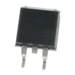
D2PAK
http://onsemi.com
for Surface Mount
Features
• Lead Formed for Surface Mount Applications in Plastic Sleeves
•
•
•
(No Suffix)
Electrically the Same as TIP41 and T1P42 Series
NJV Prefix for Automotive and Other Applications Requiring
Unique Site and Control Change Requirements; AEC−Q101
Qualified and PPAP Capable
Pb−Free Packages are Available
COMPLEMENTARY SILICON
POWER TRANSISTORS
6 AMPERES,
100 VOLTS, 65 WATTS
MARKING
DIAGRAM
D2PAK
CASE 418B
STYLE 1
MAXIMUM RATINGS
ÎÎÎÎÎÎÎÎÎÎÎÎÎÎÎÎÎÎÎÎÎÎ
ÎÎÎÎÎÎÎÎÎÎÎÎÎÎÎÎÎÎÎÎÎÎ
ÎÎÎÎÎÎÎÎÎÎÎÎÎÎÎÎÎÎÎÎÎÎ
ÎÎÎÎÎÎÎÎÎÎÎÎÎÎÎÎÎÎÎÎÎÎ
ÎÎÎÎÎÎÎÎÎÎÎÎÎÎÎÎÎÎÎÎÎÎ
ÎÎÎÎÎÎÎÎÎÎÎÎÎÎÎÎÎÎÎÎÎÎ
ÎÎÎÎÎÎÎÎÎÎÎÎÎÎÎÎÎÎÎÎÎÎ
ÎÎÎÎÎÎÎÎÎÎÎÎÎÎÎÎÎÎÎÎÎÎ
ÎÎÎÎÎÎÎÎÎÎÎÎÎÎÎÎÎÎÎÎÎÎ
ÎÎÎÎÎÎÎÎÎÎÎÎÎÎÎÎÎÎÎÎÎÎ
ÎÎÎÎÎÎÎÎÎÎÎÎÎÎÎÎÎÎÎÎÎÎ
ÎÎÎÎÎÎÎÎÎÎÎÎÎÎÎÎÎÎÎÎÎÎ
ÎÎÎÎÎÎÎÎÎÎÎÎÎÎÎÎÎÎÎÎÎÎ
ÎÎÎÎÎÎÎÎÎÎÎÎÎÎÎÎÎÎÎ
ÎÎÎÎÎÎÎÎÎÎÎÎÎÎÎÎÎÎÎ
ÎÎÎÎÎÎÎÎÎÎÎÎ
ÎÎÎÎÎÎÎÎÎÎ
ÎÎÎÎÎÎÎÎÎÎÎÎÎÎÎÎÎÎÎÎÎÎ
ÎÎÎÎÎÎÎÎÎÎÎÎÎÎÎÎÎÎÎÎÎÎ
ÎÎÎÎÎÎÎÎÎÎÎÎÎÎÎÎÎÎÎÎÎÎ
ÎÎÎÎÎÎÎÎÎÎÎÎÎÎÎÎÎÎÎÎÎÎ
ÎÎÎÎÎÎÎÎÎÎÎÎ
ÎÎÎ
ÎÎÎÎ
ÎÎÎ
ÎÎÎÎÎÎÎÎÎÎÎÎÎÎÎÎÎÎÎÎÎÎ
ÎÎÎÎÎÎÎÎÎÎÎÎÎÎÎÎÎÎÎÎÎÎ
Rating
Symbol
Value
Unit
VCEO
100
Vdc
Collector−Base Voltage
VCB
100
Vdc
Emitter−Base Voltage
VEB
5.0
Vdc
IC
6.0
10
Adc
Base Current
IB
2.0
Adc
Total Power Dissipation
@ TC = 25_C
Derate above 25_C
PD
65
0.52
W
W/_C
Total Power Dissipation
@ TA = 25_C
Derate above 25_C
PD
2.0
0.016
W
W/_C
Unclamped Inductive Load Energy (Note 1)
E
62.5
mJ
TJ, Tstg
−65 to +150
_C
Collector−Emitter Voltage
Collector Current
− Continuous
− Peak
Operating and Storage Junction
Temperature Range
THERMAL CHARACTERISTICS
Characteristic
Symbol
Max
Unit
Thermal Resistance, Junction−to−Case
RqJC
1.92
_C/W
Thermal Resistance,
Junction−to−Ambient
RqJA
62.5
_C/W
Thermal Resistance,
Junction−to−Ambient (Note 2)
RqJA
50
_C/W
Maximum Lead Temperature for Soldering
Purposes, 1/8″ from Case for 10 Seconds
TL
260
_C
J4xC
A
Y
WW
G
J4xCG
AYWW
= Specific Device Code
x = 1 or 2
= Assembly Location
= Year
= Work Week
= Pb−Free Package
ORDERING INFORMATION
Package
Shipping†
MJB41CG
D2PAK
(Pb−Free)
50 Units / Rail
MJB41CT4G
D2PAK
(Pb−Free)
800 / Tape &
Reel
NJVMJB41CT4G
D2PAK
(Pb−Free)
800 / Tape &
Reel
MJB42CG
D2PAK
(Pb−Free)
50 Units / Rail
MJB42CT4G
D2PAK
(Pb−Free)
800 / Tape &
Reel
NJVMJB42CT4G
D2PAK
(Pb−Free)
800 / Tape &
Reel
Device
†For information on tape and reel specifications,
including part orientation and tape sizes, please
refer to our Tape and Reel Packaging Specifications
Brochure, BRD8011/D.
Stresses exceeding Maximum Ratings may damage the device. Maximum
Ratings are stress ratings only. Functional operation above the Recommended
Operating Conditions is not implied. Extended exposure to stresses above the
Recommended Operating Conditions may affect device reliability.
1. IC = 2.5 A, L = 20 mH, P.R.F. = 10 Hz, VCC = 10 V, RBE = 100 W
2. When surface mounted to an FR−4 board using the minimum recommended
pad size.
© Semiconductor Components Industries, LLC, 2013
May, 2013 − Rev. 4
1
Publication Order Number:
MJB41C/D
�MJB41C, NJVMJB41CT4G (NPN), MJB42C, NJVMJB42CT4G (PNP)
ÎÎÎÎÎÎÎÎÎÎÎÎÎÎÎÎÎÎÎÎÎÎÎÎÎÎÎÎÎÎÎÎÎ
ÎÎÎÎÎÎÎÎÎÎÎÎÎÎÎÎÎÎÎÎÎÎÎÎÎÎÎÎÎÎÎÎÎ
ÎÎÎÎÎÎÎÎÎÎÎÎÎÎÎÎÎÎÎÎÎÎÎ
ÎÎÎÎÎÎÎÎÎÎÎÎÎÎ
ÎÎÎÎÎÎÎÎÎÎÎÎÎÎÎÎÎÎÎÎÎÎÎÎÎÎÎÎÎÎÎÎÎÎÎÎÎ
ÎÎÎÎÎÎÎÎÎÎÎÎÎÎÎÎÎÎÎÎÎÎÎÎÎÎÎÎÎÎÎÎÎ
ÎÎÎÎÎÎÎÎÎÎÎÎÎÎÎÎÎÎÎÎÎÎÎÎÎÎÎÎÎÎÎÎÎ
ÎÎÎÎÎÎÎÎÎÎÎÎÎÎÎÎÎÎÎÎÎÎÎ
ÎÎÎÎÎÎÎÎÎÎÎÎÎÎ
ÎÎÎÎÎÎÎÎÎÎÎÎÎÎÎÎÎÎÎÎÎÎÎÎÎÎÎÎÎÎÎÎÎÎÎÎÎ
ÎÎÎÎÎÎÎÎÎÎÎÎÎÎÎÎÎÎÎÎÎÎÎÎÎÎÎÎÎÎÎÎÎÎÎÎÎ
ÎÎÎÎÎÎÎÎÎÎÎÎÎÎÎÎÎÎÎÎÎÎÎÎÎÎÎÎÎÎÎÎÎÎÎÎÎ
ÎÎÎÎÎÎÎÎÎÎÎÎÎÎÎÎÎÎÎÎÎÎÎÎÎÎÎÎÎÎÎÎÎÎÎÎÎ
ÎÎÎÎÎÎÎÎÎÎÎÎÎÎÎÎÎÎÎÎÎÎÎÎÎÎÎÎÎÎÎÎÎ
ÎÎÎÎÎÎÎÎÎÎÎÎÎÎÎÎÎÎÎÎÎÎÎÎÎÎÎÎÎÎÎÎÎ
ÎÎÎÎÎÎÎÎÎÎÎÎÎÎÎÎÎÎÎÎÎÎÎ
ÎÎÎÎÎÎÎÎÎÎÎÎÎÎ
ÎÎÎÎÎÎÎÎÎÎÎÎÎÎÎÎÎÎÎÎÎÎÎÎÎÎÎÎÎÎÎÎÎÎÎÎÎ
ÎÎÎÎÎÎÎÎÎÎÎÎÎÎÎÎÎÎÎÎÎÎÎ
ÎÎÎÎ
ÎÎÎÎ
ÎÎÎ
ÎÎÎ
ÎÎÎÎÎÎÎÎÎÎÎÎÎÎÎÎÎÎÎÎÎÎÎÎÎÎÎÎÎÎÎÎÎÎÎÎÎ
ÎÎÎÎÎÎÎÎÎÎÎÎÎÎÎÎÎÎÎÎÎÎÎÎÎÎÎÎÎÎÎÎÎ
ÎÎÎÎÎÎÎÎÎÎÎÎÎÎÎÎÎÎÎÎÎÎÎÎÎÎÎÎÎÎÎÎÎ
ÎÎÎÎÎÎÎÎÎÎÎÎÎÎÎÎÎÎÎÎÎÎÎ
ÎÎÎÎÎÎÎÎÎÎÎÎÎÎ
ÎÎÎÎÎÎÎÎÎÎÎÎÎÎÎÎÎÎÎÎÎÎÎÎÎÎÎÎÎÎÎÎÎÎÎÎÎ
ÎÎÎÎÎÎÎÎÎÎÎÎÎÎÎÎÎÎÎÎÎÎÎÎÎÎÎÎÎÎÎÎÎÎÎÎÎ
ELECTRICAL CHARACTERISTICS (TC = 25_C unless otherwise noted)
Characteristic
Symbol
Min
Max
Unit
VCEO(sus)
100
−
Vdc
Collector Cutoff Current (VCE = 60 Vdc, IB = 0)
ICEO
−
0.7
mAdc
Collector Cutoff Current (VCE = 100 Vdc, VEB = 0)
ICES
−
100
mAdc
Emitter Cutoff Current (VBE = 5.0 Vdc, IC = 0)
IEBO
−
50
mAdc
hFE
30
15
−
75
−
Collector−Emitter Saturation Voltage (IC = 6.0 Adc, IB = 600 mAdc)
VCE(sat)
−
1.5
Vdc
Base−Emitter On Voltage (IC = 6.0 Adc, VCE = 4.0 Vdc)
VBE(on)
−
2.0
Vdc
Current−Gain − Bandwidth Product (IC = 500 mAdc, VCE = 10 Vdc, ftest = 1.0 MHz)
fT
3.0
−
MHz
Small−Signal Current Gain (IC = 0.5 Adc, VCE = 10 Vdc, f = 1.0 kHz)
hfe
20
−
−
OFF CHARACTERISTICS
Collector−Emitter Sustaining Voltage (Note 3) (IC = 30 mAdc, IB = 0)
ON CHARACTERISTICS (Note 3)
DC Current Gain
(IC = 0.3 Adc, VCE = 4.0 Vdc)
(IC = 3.0 Adc, VCE = 4.0 Vdc)
DYNAMIC CHARACTERISTICS
PD, POWER DISSIPATION (WATTS)
3. Pulse Test: Pulse Width v 300 ms, Duty Cycle v 2.0%.
TA
4.0
TC
80
3.0
60
2.0
40
1.0
20
0
0
TC
TA
0
20
40
60
100
80
T, TEMPERATURE (°C)
120
140
160
Figure 1. Power Derating
VCC
+�30 V
2.0
RC
0.7
0.5
SCOPE
+11 V
-�9.0 V
tr, tf ≤ 10 ns
DUTY CYCLE = 1.0%
t, TIME (��s)
μ
RB
0
TJ = 25°C
VCC = 30 V
IC/IB = 10
1.0
25 ms
D1
0.3
0.2
tr
0.1
0.07
0.05
-�4 V
RB and RC VARIED TO OBTAIN DESIRED CURRENT LEVELS
0.03
0.02
0.06
D1 MUST BE FAST RECOVERY TYPE, e.g.:
��1N5825 USED ABOVE IB ≈ 100 mA
��MSD6100 USED BELOW IB ≈ 100 mA
td @ VBE(off) ≈ 5.0 V
0.1
1.0
0.2
2.0
0.4 0.6
IC, COLLECTOR CURRENT (AMP)
Figure 3. Turn−On Time
Figure 2. Switching Time Test Circuit
http://onsemi.com
2
4.0
6.0
�r(t), TRANSIENT THERMAL RESISTANCE (NORMALIZED)
MJB41C, NJVMJB41CT4G (NPN), MJB42C, NJVMJB42CT4G (PNP)
1.0
0.7
0.5
D = 0.5
0.3
0.2
0.2
0.1
0.1
0.07
0.05
0.02
0.03
0.02
0.01
SINGLE PULSE
0.01
0.01
0.02
0.05
1.0
P(pk)
ZqJC(t) = r(t) RqJC
RqJC = 1.92°C/W MAX
D CURVES APPLY FOR POWER
PULSE TRAIN SHOWN
READ TIME AT t1
TJ(pk) - TC = P(pk) ZqJC(t)
0.05
0.2
0.5
2.0
5.0
t, TIME (ms)
1.0
10
20
t1
t2
DUTY CYCLE, D = t1/t2
50
100
200
500
1.0 k
Figure 4. Thermal Response
10
There are two limitations on the power handling ability of
a transistor: average junction temperature and second
breakdown. Safe operating area curves indicate IC − VCE
limits of the transistor that must be observed for reliable
operation; i.e., the transistor must not be subjected to greater
dissipation than the curves indicate.
The data of Figure 5 is based on TJ(pk) = 150_C; TC is
variable depending on conditions. Second breakdown pulse
limits are valid for duty cycles to 10% provided TJ(pk)
v 150_C. TJ(pk) may be calculated from the data in
Figure 4. At high case temperatures, thermal limitations will
reduce the power that can be handled to values less than the
limitations imposed by second breakdown.
IC, COLLECTOR CURRENT (AMP)
0.5�ms
5.0
1.0�ms
3.0
2.0
1.0
0.5
0.3
0.2
SECONDARY BREAKDOWN LTD
BONDING WIRE LTD
THERMAL LIMITATION @ TC = 25°C
(SINGLE PULSE)
CURVES APPLY BELOW RATED VCEO
0.1
5.0
5.0�ms
40
10
20
60
VCE, COLLECTOR-EMITTER VOLTAGE (VOLTS)
80 100
Figure 5. Active−Region Safe Operating Area
5.0
300
ts
t, TIME (��s)
μ
1.0
TJ = 25°C
TJ = 25°C
VCC = 30 V
IC/IB = 10
IB1 = IB2
200
C, CAPACITANCE (pF)
3.0
2.0
0.7
0.5
0.3
0.2
0.1
0.07
0.05
0.06
tf
Cib
100
70
Cob
50
0.1
0.2
0.4 0.6
1.0
2.0
IC, COLLECTOR CURRENT (AMP)
4.0
30
0.5
6.0
Figure 6. Turn−Off Time
1.0
2.0 3.0
5.0
10
20
VR, REVERSE VOLTAGE (VOLTS)
Figure 7. Capacitance
http://onsemi.com
3
30
50
�MJB41C, NJVMJB41CT4G (NPN), MJB42C, NJVMJB42CT4G (PNP)
hFE, DC CURRENT GAIN
300
200
VCE = 2.0 V
TJ = 150°C
100
70
50
25°C
30
20
10
7.0
5.0
0.06
VCE , COLLECTOR-EMITTER VOLTAGE (VOLTS)
500
-�55°C
4.0
1.0
2.0
0.2 0.3 0.4 0.6
IC, COLLECTOR CURRENT (AMP)
0.1
2.0
TJ = 25°C
1.6
1.2
IC = 1.0 A
0.4
0
10
6.0
θV, TEMPERATURE COEFFICIENTS (mV/°C)
V, VOLTAGE (VOLTS)
1.6
1.2
VBE(sat) @ IC/IB = 10
0.8
VBE @ VCE = 4.0 V
0.4
VCE(sat) @ IC/IB = 10
0.2 0.3 0.4
IC, COLLECTOR CURRENT (��A)
μ
50
100
200 300
IB, BASE CURRENT (mA)
500
0.6
2.0 3.0 4.0
1.0
6.0
1000
*APPLIES FOR IC/IB ≤ hFE/4
+�1.5
+�1.0
+�25°C to +�150°C
+�0.5
*�qVC FOR VCE(sat)
0
-�55°C to +�25°C
-�0.5
+�25°C to +�150°C
-�1.0
-�1.5
qVB FOR VBE
-�55°C to +�25°C
-�2.0
-�2.5
0.06
0.1
0.2 0.3
0.5
1.0
2.0 3.0 4.0
IC, COLLECTOR CURRENT (AMP)
Figure 10. “On” Voltages
Figure 11. Temperature Coefficients
VCE = 30 V
TJ = 150°C
100°C
25°C
100
IC = ICES
10-1
REVERSE
10-3
-�0.3 -�0.2 -�0.1
+�2.0
IC, COLLECTOR CURRENT (AMP)
R BE , EXTERNAL BASE-EMITTER RESISTANCE (OHMS)
0.1
103
10-2
30
+�2.5
TJ = 25°C
101
20
Figure 9. Collector Saturation Region
2.0
102
5.0 A
0.8
Figure 8. DC Current Gain
0
0.06
2.5 A
FORWARD
0
+�0.1 +�0.2 +�0.3 +�0.4 +�0.5 +�0.6
+�0.7
6.0
10�M
VCE = 30 V
1.0�M
IC = 10 x ICES
IC ≈ ICES
100�k
10�k
IC = 2 x ICES
1.0�k
0.1�k
(TYPICAL ICES VALUES
OBTAINED FROM FIGURE 12)
20
40
60
80
100
120
140
160
VBE, BASE-EMITTER VOLTAGE (VOLTS)
TJ, JUNCTION TEMPERATURE (°C)
Figure 12. Collector Cut−Off Region
Figure 13. Effects of Base−Emitter Resistance
http://onsemi.com
4
�MECHANICAL CASE OUTLINE
PACKAGE DIMENSIONS
D2PAK 3
CASE 418B−04
ISSUE L
DATE 17 FEB 2015
SCALE 1:1
NOTES:
1. DIMENSIONING AND TOLERANCING
PER ANSI Y14.5M, 1982.
2. CONTROLLING DIMENSION: INCH.
3. 418B−01 THRU 418B−03 OBSOLETE,
NEW STANDARD 418B−04.
C
E
−B−
V
W
4
1
2
A
S
3
−T−
SEATING
PLANE
K
W
J
G
D
DIM
A
B
C
D
E
F
G
H
J
K
L
M
N
P
R
S
V
H
3 PL
0.13 (0.005)
M
T B
M
VARIABLE
CONFIGURATION
ZONE
N
R
P
L
M
STYLE 1:
PIN 1. BASE
2. COLLECTOR
3. EMITTER
4. COLLECTOR
L
M
F
F
F
VIEW W−W
1
VIEW W−W
2
VIEW W−W
3
STYLE 2:
PIN 1. GATE
2. DRAIN
3. SOURCE
4. DRAIN
MILLIMETERS
MIN
MAX
8.64
9.65
9.65 10.29
4.06
4.83
0.51
0.89
1.14
1.40
7.87
8.89
2.54 BSC
2.03
2.79
0.46
0.64
2.29
2.79
1.32
1.83
7.11
8.13
5.00 REF
2.00 REF
0.99 REF
14.60 15.88
1.14
1.40
U
L
M
INCHES
MIN
MAX
0.340 0.380
0.380 0.405
0.160 0.190
0.020 0.035
0.045 0.055
0.310 0.350
0.100 BSC
0.080
0.110
0.018 0.025
0.090
0.110
0.052 0.072
0.280 0.320
0.197 REF
0.079 REF
0.039 REF
0.575 0.625
0.045 0.055
STYLE 3:
PIN 1. ANODE
2. CATHODE
3. ANODE
4. CATHODE
STYLE 4:
PIN 1. GATE
2. COLLECTOR
3. EMITTER
4. COLLECTOR
STYLE 5:
STYLE 6:
PIN 1. CATHODE
PIN 1. NO CONNECT
2. ANODE
2. CATHODE
3. CATHODE
3. ANODE
4. ANODE
4. CATHODE
MARKING INFORMATION AND FOOTPRINT ON PAGE 2
DOCUMENT NUMBER:
DESCRIPTION:
98ASB42761B
D2PAK 3
Electronic versions are uncontrolled except when accessed directly from the Document Repository.
Printed versions are uncontrolled except when stamped “CONTROLLED COPY” in red.
PAGE 1 OF 2
ON Semiconductor and
are trademarks of Semiconductor Components Industries, LLC dba ON Semiconductor or its subsidiaries in the United States and/or other countries.
ON Semiconductor reserves the right to make changes without further notice to any products herein. ON Semiconductor makes no warranty, representation or guarantee regarding
the suitability of its products for any particular purpose, nor does ON Semiconductor assume any liability arising out of the application or use of any product or circuit, and specifically
disclaims any and all liability, including without limitation special, consequential or incidental damages. ON Semiconductor does not convey any license under its patent rights nor the
rights of others.
© Semiconductor Components Industries, LLC, 2019
www.onsemi.com
�D2PAK 3
CASE 418B−04
ISSUE L
DATE 17 FEB 2015
GENERIC
MARKING DIAGRAM*
xx
xxxxxxxxx
AWLYWWG
xxxxxxxxG
AYWW
AYWW
xxxxxxxxG
AKA
IC
Standard
Rectifier
xx
A
WL
Y
WW
G
AKA
= Specific Device Code
= Assembly Location
= Wafer Lot
= Year
= Work Week
= Pb−Free Package
= Polarity Indicator
*This information is generic. Please refer to
device data sheet for actual part marking.
Pb−Free indicator, “G” or microdot “ G”,
may or may not be present.
SOLDERING FOOTPRINT*
10.49
8.38
16.155
2X
3.504
2X
1.016
5.080
PITCH
DIMENSIONS: MILLIMETERS
*For additional information on our Pb−Free strategy and soldering
details, please download the ON Semiconductor Soldering and
Mounting Techniques Reference Manual, SOLDERRM/D.
DOCUMENT NUMBER:
DESCRIPTION:
98ASB42761B
D2PAK 3
Electronic versions are uncontrolled except when accessed directly from the Document Repository.
Printed versions are uncontrolled except when stamped “CONTROLLED COPY” in red.
PAGE 2 OF 2
ON Semiconductor and
are trademarks of Semiconductor Components Industries, LLC dba ON Semiconductor or its subsidiaries in the United States and/or other countries.
ON Semiconductor reserves the right to make changes without further notice to any products herein. ON Semiconductor makes no warranty, representation or guarantee regarding
the suitability of its products for any particular purpose, nor does ON Semiconductor assume any liability arising out of the application or use of any product or circuit, and specifically
disclaims any and all liability, including without limitation special, consequential or incidental damages. ON Semiconductor does not convey any license under its patent rights nor the
rights of others.
© Semiconductor Components Industries, LLC, 2019
www.onsemi.com
�onsemi,
, and other names, marks, and brands are registered and/or common law trademarks of Semiconductor Components Industries, LLC dba “onsemi” or its affiliates
and/or subsidiaries in the United States and/or other countries. onsemi owns the rights to a number of patents, trademarks, copyrights, trade secrets, and other intellectual property.
A listing of onsemi’s product/patent coverage may be accessed at www.onsemi.com/site/pdf/Patent−Marking.pdf. onsemi reserves the right to make changes at any time to any
products or information herein, without notice. The information herein is provided “as−is” and onsemi makes no warranty, representation or guarantee regarding the accuracy of the
information, product features, availability, functionality, or suitability of its products for any particular purpose, nor does onsemi assume any liability arising out of the application or use
of any product or circuit, and specifically disclaims any and all liability, including without limitation special, consequential or incidental damages. Buyer is responsible for its products
and applications using onsemi products, including compliance with all laws, regulations and safety requirements or standards, regardless of any support or applications information
provided by onsemi. “Typical” parameters which may be provided in onsemi data sheets and/or specifications can and do vary in different applications and actual performance may
vary over time. All operating parameters, including “Typicals” must be validated for each customer application by customer’s technical experts. onsemi does not convey any license
under any of its intellectual property rights nor the rights of others. onsemi products are not designed, intended, or authorized for use as a critical component in life support systems
or any FDA Class 3 medical devices or medical devices with a same or similar classification in a foreign jurisdiction or any devices intended for implantation in the human body. Should
Buyer purchase or use onsemi products for any such unintended or unauthorized application, Buyer shall indemnify and hold onsemi and its officers, employees, subsidiaries, affiliates,
and distributors harmless against all claims, costs, damages, and expenses, and reasonable attorney fees arising out of, directly or indirectly, any claim of personal injury or death
associated with such unintended or unauthorized use, even if such claim alleges that onsemi was negligent regarding the design or manufacture of the part. onsemi is an Equal
Opportunity/Affirmative Action Employer. This literature is subject to all applicable copyright laws and is not for resale in any manner.
PUBLICATION ORDERING INFORMATION
LITERATURE FULFILLMENT:
Email Requests to: orderlit@onsemi.com
onsemi Website: www.onsemi.com
◊
TECHNICAL SUPPORT
North American Technical Support:
Voice Mail: 1 800−282−9855 Toll Free USA/Canada
Phone: 011 421 33 790 2910
Europe, Middle East and Africa Technical Support:
Phone: 00421 33 790 2910
For additional information, please contact your local Sales Representative
�