NL17SV08XV5T2 Single 2−Input AND Gate
The NL17SV08 is an ultra−high performance 2−Input AND gate manufactured in 0.35m CMOS technology with excellent performance down to 0.9 volts. This device is ideal for extremely high−speed and high−drive applications. Additionally, limitations of board space are no longer a constraint. The very small SOT−553 makes this device fit most tight designs and spaces.
Features
http://onsemi.com MARKING DIAGRAM
5 1
• • • • • • • • • • •
Extremely High Speed: tPD = 1.0 ns (Typ) @ VCC = 3.3 V Designed for 0.9 to 3.3 V Operation Overvoltage Tolerance (OVT)* Input Pins Permit Logic Translation Balanced "24 mA Output Drive @ 3.3 V Near Zero Static Supply Current Ultra−Tiny SOT−553 5 Pin Package Only 1.6 x 1.6 x 0.6 mm All Devices in Package SOT−553 are Inherently Pb−Free
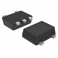
SOT−553 CASE 463B
UG M G G
Typical Applications
UG = Specific Device Code M = Date Code G = Pb−Free Package (Note: Microdot may be in either location)
Cellular Digital Camera PDA Digital Video
PIN DIAGRAM
IN A 1 5 VCC
Industry Standard
IN B
2
• Functionally Similar to NC7SV08 and SN74AUC1G08
GND 3 4 OUT Y
PIN ASSIGNMENT
PIN # 1 2 3 4 5 FUNCTION IN A IN B GND OUT Y VCC
FUNCTION TABLE
Input A L L H H Input B L H L H Output Y L L L H
ORDERING INFORMATION
*Overvoltage Tolerance (OVT) enables input pins to function outside (higher) of their operating voltages, with no damage to the devices or to signal integrity.
© Semiconductor Components Industries, LLC, 2005
See detailed ordering and shipping information in the package dimensions section on page 4 of this data sheet.
1
October, 2005 − Rev. 4
Publication Order Number: NL17SV08XV5T2/D
�NL17SV08XV5T2
MAXIMUM RATINGS
Symbol VCC VI VO IIK IOK IO ICC IGND TSTG TL TJ qJA PD MSL FR DC Supply Voltage DC Input Voltage DC Output Voltage DC Input Diode Current DC Output Diode Current DC Output Sink Current DC Supply Current per Supply Pin DC Ground Current per Ground Pin Storage Temperature Range Lead Temperature, 1.0 mm from Case for 10 seconds Junction Temperature Under Bias Thermal Resistance (Note 1) Power Dissipation in Still Air at 85°C Moisture Sensitivity Flammability Rating Oxygen Index: 28 to 34 VI < GND VO = GND VO = VCC Rating Value −0.5 to + 4.6 −0.5 to + 4.6 −0.5 to VCC +0.5 ±50 −50 +50 ±50 ±50 ±50 − 65 to +150 260 +150 250 250 Level 1 UL 94 V−0 @ 0.125 in Unit V V V mA mA mA mA mA °C °C °C °C/W mW
Maximum ratings are those values beyond which device damage can occur. Maximum ratings applied to the device are individual stress limit values (not normal operating conditions) and are not valid simultaneously. If these limits are exceeded, device functional operation is not implied, damage may occur and reliability may be affected. 1. Measured with minimum pad spacing on an FR4 board, using 10 mm−by−1 inch, 2 ounce copper trace no air flow.
RECOMMENDED OPERATING CONDITIONS
Symbol VCC VIN Vout IOH/IOL Positive DC Supply Voltage Digital Input Voltage Output Voltage Output Current VCC = 3.0 V to 3.6 V VCC = 2.3 V to 2.7 V VCC = 1.65 V to 1.95 V VCC = 1.4 V to 1.6 V VCC = 1.1 V to 1.3 V VCC = 0.9 V −40 VCC = 3.3V ± 0.3 V 0 Parameter Min 0.9 0 0 Max 3.6 3.6 VCC ±24 ±18 ±6 ±4 ±2 ±0.1 +85 10 Unit V V V mA
tA tr, tf
Operating Temperature Range. All Package Types Input Rise or Fall Time
°C nS/V
DEVICE JUNCTION TEMPERATURE VERSUS TIME TO 0.1% BOND FAILURES
Junction Temperature °C 80 90 100 110 120 130 140 Time, Hours 1,032,200 419,300 178,700 79,600 37,000 17,800 8,900 Time, Years 117.8 47.9 20.4 9.4 4.2 2.0 1.0
http://onsemi.com
2
�NL17SV08XV5T2
DC CHARACTERISTICS– Digital Section (Voltages Referenced to GND)
TA = 25°C Symbol VIH Parameter High Level Input Voltage Condition VCC 0.90 1.10 v= VCC v 1.30 1.40 v VCC v 1.60 1.65 v VCC v 1.95 2.30 v VCC v 2.70 2.70 v VCC v 3.60 0.90 1.10 v VCC v 1.30 1.40 v VCC v 1.60 1.65 v VCC v 1.95 2.30 v VCC v 2.70 2.70 v VCC v 3.60 IOH = −100 mA 0.90 1.10 v VCC v 1.30 1.40 v VCC v 1.60 1.65 v VCC v 1.95 2.30 v VCC v 2.70 2.70 v VCC v 3.60 1.10 v VCC v 1.30 1.40 v VCC v 1.60 1.65 v VCC v 1.95 2.30 v VCC v 2.70 2.30 v VCC v 2.70 2.70 v VCC v 3.60 2.30 v VCC v 2.70 2.70 v VCC v 3.60 2.70 v VCC v 3.60 0.90 1.10 v VCC v 1.30 1.40 v VCC v 1.60 1.65 v VCC v 1.95 2.30 v VCC v 2.70 2.70 v VCC v 3.60 1.10 v VCC v 1.30 1.40 v VCC v 1.60 1.65 v VCC v 1.95 2.30 v VCC v 2.70 2.70 v VCC v 3.60 2.30 v VCC v 2.70 2.70 v VCC v 3.60 2.70 v VCC v 3.60 0.90 to 3.60 0 VI = VCC or GND 0.90 to 3.60 VCC − 0.1 VCC − 0.1 VCC − 0.2 VCC − 0.2 VCC − 0.2 VCC − 0.2 0.75 x VCC 0.75 x VCC 1.25 2.0 1.8 2.2 1.7 2.4 2.2 0.1 0.1 0.2 0.2 0.2 0.2 0.25 x VCC 0.25 x VCC 0.3 0.4 0.4 0.6 0.4 0.55 ±0.1 10 0.9 Min 0.65 x VCC 0.65 x VCC 0.65 x VCC 0.65 x VCC 1.6 2.0 0.35 x VCC 0.35 x VCC 0.35 x VCC 0.35 x VCC 0.7 0.8 VCC − 0.1 VCC − 0.1 VCC − 0.2 VCC − 0.2 VCC − 0.2 VCC − 0.2 0.75 x VCC 0.75 x VCC 1.25 2.0 1.8 2.2 1.7 2.4 2.2 0.1 0.1 0.2 0.2 0.2 0.2 0.25 x VCC 0.25 x VCC 0.3 0.4 0.4 0.6 0.4 0.55 ±0.9 10 5 mA mA mA V Max TA = −40 to 85°C Min 0.65 x VCC 0.65 x VCC 0.65 x VCC 0.65 x VCC 1.6 2.0 0.35 x VCC 0.35 x VCC 0.35 x VCC 0.35 x VCC 0.7 0.8 Max Unit V
VIL
Low Level Input Voltage
V
VOH
High Level Output Voltage
V
IOH = −2.0 mA IOH = −4.0 mA IOH = −6.0 mA IOH = −12 mA IOH = −18 mA IOH = −24 mA VOL Low Level Output Voltage IOL = 100 mA
IOL = 2.0 mA IOL = 4.0 mA IOL = 6.0 mA IOL = 12 mA IOL = 18 mA IOL = 24 mA IIN IOFF ICC Input Leakage Current Power Off Leakage Current Quiescent Supply Current 0 = VI = 3.6 V
http://onsemi.com
3
�NL17SV08XV5T2
AC CHARACTERISTICS (Input tr = tf = 3.0 nS)
−40°C Symbol TPHL, TPLH Parameter Propagation Delay Condition CL = 15 pF, RL = 1.0 MW CL = 15 pF, RL = 2.0 kW CL = 30 pF, RL = 500 kW VCC 0.90 1.10 v VCC v 1.30 1.40 v VCC v 1.60 1.65 v VCC v 1.95 2.30 v VCC v 2.70 2.70 v VCC v 3.60 0 0 VI = 0 V or VCC F = 10 MHz 0.90 to 3.60 3.0 1.0 1.0 0.8 0.7 Min 25°C Typ 13 6.0 3.2 2.0 1.2 1.0 2.0 4.5 20 10.0 6.0 4.5 2.6 2.3 1.0 1.0 1.0 0.7 0.6 14.6 7.2 5.3 3.7 3.0 Max 85°C Min Max Unit nS nS nS
CIN COUT CPD
Input Capacitance Output Capacitance Power Dissipation Capacitance
pF pF pF
ORDERING INFORMATION
Device Order Number NL17SV08XV5T2 NL17SV08XV5T2G Package Type SOT−553* SOT−553* Shipping† 178 mm, 4000 Units / Tape & Reel 178 mm, 4000 Units / Tape & Reel
†For information on tape and reel specifications, including part orientation and tape sizes, please refer to our Tape and Reel Packaging Specifications Brochure, BRD8011/D. *This package is inherently Pb−Free.
http://onsemi.com
4
�NL17SV08XV5T2
PACKAGE DIMENSIONS
SOT−553 5−LEAD PACKAGE CASE 463B−01 ISSUE B
D −X−
A L
4
5
1
2
3
E −Y−
HE
NOTES: 1. DIMENSIONING AND TOLERANCING PER ANSI Y14.5M, 1982. 2. CONTROLLING DIMENSION: MILLIMETERS 3. MAXIMUM LEAD THICKNESS INCLUDES LEAD FINISH THICKNESS. MINIMUM LEAD THICKNESS IS THE MINIMUM THICKNESS OF BASE MATERIAL. DIM A b c D E e L HE MILLIMETERS NOM MAX 0.55 0.60 0.22 0.27 0.13 0.18 1.60 1.70 1.20 1.30 0.50 BSC 0.10 0.20 0.30 1.50 1.60 1.70 MIN 0.50 0.17 0.08 1.50 1.10 MIN 0.020 0.007 0.003 0.059 0.043 INCHES NOM 0.022 0.009 0.005 0.063 0.047 0.020 BSC 0.004 0.008 0.059 0.063 MAX 0.024 0.011 0.007 0.067 0.051 0.012 0.067
e
b 5 PL 0.08 (0.003)
c
M
XY
SOLDERING FOOTPRINT*
0.3 0.0118 0.45 0.0177 1.0 0.0394
1.35 0.0531
0.5 0.5 0.0197 0.0197
SCALE 20:1 mm inches
*For additional information on our Pb−Free strategy and soldering details, please download the ON Semiconductor Soldering and Mounting Techniques Reference Manual, SOLDERRM/D.
ON Semiconductor and are registered trademarks of Semiconductor Components Industries, LLC (SCILLC). SCILLC reserves the right to make changes without further notice to any products herein. SCILLC makes no warranty, representation or guarantee regarding the suitability of its products for any particular purpose, nor does SCILLC assume any liability arising out of the application or use of any product or circuit, and specifically disclaims any and all liability, including without limitation special, consequential or incidental damages. “Typical” parameters which may be provided in SCILLC data sheets and/or specifications can and do vary in different applications and actual performance may vary over time. All operating parameters, including “Typicals” must be validated for each customer application by customer’s technical experts. SCILLC does not convey any license under its patent rights nor the rights of others. SCILLC products are not designed, intended, or authorized for use as components in systems intended for surgical implant into the body, or other applications intended to support or sustain life, or for any other application in which the failure of the SCILLC product could create a situation where personal injury or death may occur. Should Buyer purchase or use SCILLC products for any such unintended or unauthorized application, Buyer shall indemnify and hold SCILLC and its officers, employees, subsidiaries, affiliates, and distributors harmless against all claims, costs, damages, and expenses, and reasonable attorney fees arising out of, directly or indirectly, any claim of personal injury or death associated with such unintended or unauthorized use, even if such claim alleges that SCILLC was negligent regarding the design or manufacture of the part. SCILLC is an Equal Opportunity/Affirmative Action Employer. This literature is subject to all applicable copyright laws and is not for resale in any manner.
PUBLICATION ORDERING INFORMATION
LITERATURE FULFILLMENT: N. American Technical Support: 800−282−9855 Toll Free Literature Distribution Center for ON Semiconductor USA/Canada P.O. Box 61312, Phoenix, Arizona 85082−1312 USA Phone: 480−829−7710 or 800−344−3860 Toll Free USA/Canada Japan : ON Semiconductor, Japan Customer Focus Center 2−9−1 Kamimeguro, Meguro−ku, Tokyo, Japan 153−0051 Fax: 480−829−7709 or 800−344−3867 Toll Free USA/Canada Phone: 81−3−5773−3850 Email: orderlit@onsemi.com ON Semiconductor Website: http://onsemi.com Order Literature: http://www.onsemi.com/litorder For additional information, please contact your local Sales Representative.
http://onsemi.com
5
NL17SV08XV5T2/D
�


 工商网监
湘ICP备2023018690号
工商网监
湘ICP备2023018690号
