NL7WB66
Ultra-Small SPST Analog
Switch
The NL7WB66 is a very low RON dual SPST analog switch. RON is
5.0 � (Typ) at 5.0 V. The device is offered in the very popular low cost
US8 package. It is designed as a general purpose dual switch and can
be used to switch either analog signals such as audio and video or
digital signal such as TTL, CMOS, LVDS, ECL, or complex digital
signals such as QPSK.
www.onsemi.com
MARKING
DIAGRAM
Features
•
•
•
•
•
•
•
•
•
•
•
8
Excellent Performance RDSON = 5.0 � at 5.0 V
High Speed Operation: tPD = 0.25 ns (Max) at 5.0 V
1.65 to 5.5 V Operating Range
Reduced Threshold Voltages for LVTTL on Control Pin
♦ Eliminates the Need for Translators for Many Applications
♦ TTL Compatibility when VCC is 5.0 V
♦ Can Operate with 1.8 V Inputs, if VCC is 3.0
♦ Also Meets Full CMOS Specifications
Ultra−Low Charge Injection = 7.5 pC at 5.0 V
Low Stand−by Power ICC = 1.0 nA (Max) at TA = 25°C
Control Pins IN1, IN2, are Overvoltage Tolerant
Pin for Pin Replacement TC7WB66, NC7WB66, 74LVC2G66
ESD Protection:
Machine Model >200 V,
Human Body Model >2000 V
Latchup Max Rating: 200 mA
These Devices are Pb−Free, Halogen Free/BFR Free and are RoHS
Compliant
Typical Applications
•
•
•
•
•
Cell Phones
PDAs
Digital Still Cameras
Video
Digital Video
NO1
1
8
VCC
2
7
OE1
OE2
3
6
COM2
4
1
AJ M G
G
1
AJ
M
G
= Device Code
= Date Code*
= Pb−Free Package
(Note: Microdot may be in either location)
*Date Code orientation may vary depending upon manufacturing location.
PIN ASSIGNMENT
Pin
Function
OVT
1
NO1
−
2
COM1
−
3
OE2
Yes
4
GND
−
5
NO2
−
6
COM2
−
7
OE1
Yes
8
VCC
−
FUNCTION TABLE
COM1
GND
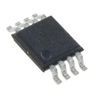
US8
US SUFFIX
CASE 493
8
5
On/Off
Enable Input
State of
Analog Switch
L
H
Off
On
ORDERING INFORMATION
See detailed ordering and shipping information in the package
dimensions section on page 5 of this data sheet.
NO2
Figure 1. Pin Assignment Diagram
© Semiconductor Components Industries, LLC, 2015
July, 2015 − Rev. 6
1
Publication Order Number:
NL7WB66/D
�NL7WB66
MAXIMUM RATINGS
Symbol
Value
Unit
DC Supply Voltage
*0.5 to )7.0
V
VI
DC Input Voltage
*0.5 to )7.0
V
VO
DC Output Voltage
*0.5 to )7.0
V
VI < GND
*50
mA
VO < GND
*50
mA
VCC
Rating
IIK
DC Input Diode Current
IOK
DC Output Diode Current
IO
DC Output Sink Current
$50
mA
ICC
DC Supply Current per Supply Pin
$100
mA
IGND
DC Ground Current per Ground Pin
$100
mA
TSTG
Storage Temperature Range
*65 to )150
°C
260
°C
)150
°C
Thermal Resistance
250
°C/W
Power Dissipation in Still Air at 85°C
250
mW
Level 1
−
UL 94 V−0 @ 0.125 in
−
> 2000
> 200
N/A
V
TL
Lead Temperature, 1 mm from Case for 10 Seconds
TJ
Junction Temperature under Bias
�JA
PD
MSL
Moisture Sensitivity
FR
Flammability Rating
VESD
Oxygen Index: 28 to 34
ESD Withstand Voltage
Human Body Model (Note 2)
Machine Model (Note 3)
Charged Device Model (Note 4)
Stresses exceeding those listed in the Maximum Ratings table may damage the device. If any of these limits are exceeded, device functionality
should not be assumed, damage may occur and reliability may be affected.
1. Measured with minimum pad spacing on an FR4 board, using 10 mm−by−1 inch, 2−ounce copper trace with no air flow.
2. Tested to EIA/JESD22−A114−A.
3. Tested to EIA/JESD22−A115−A.
4. Tested to JESD22−C101−A.
RECOMMENDED OPERATING CONDITIONS
Symbol
Characteristics
Min
Max
Unit
VCC
Positive DC Supply Voltage
1.65
5.5
V
VIN
Digital Input Voltage (Enable)
GND
5.5
V
VIO
Static or Dynamic Voltage Across an Off Switch
GND
VCC
V
VIS
Analog Input Voltage
GND
VCC
V
TA
Operating Temperature Range, All Package Types
−55
+125
°C
tr, tf
Input Rise or Fall Time
(Enable Input)
0
0
100
20
ns/V
NO
COM
VCC = 3.3 V + 0.3 V
VCC = 5.0 V + 0.5 V
Functional operation above the stresses listed in the Recommended Operating Ranges is not implied. Extended exposure to stresses beyond
the Recommended Operating Ranges limits may affect device reliability.
DEVICE JUNCTION TEMPERATURE VS. TIME TO
0.1% BOND FAILURES
Junction
Temperature 5C
Time, Hours
Time, Years
80
90
100
110
1,032,200
419,300
178,700
79,600
117.8
47.9
20.4
9.4
120
37,000
4.2
130
17,800
2.0
140
8,900
1.0
www.onsemi.com
2
�TJ = 80°C
TJ = 90°C
TJ = 100°C
TJ = 110°C
TJ = 120°C
FAILURE RATE OF PLASTIC = CERAMIC
UNTIL INTERMETALLICS OCCUR
TJ = 130°C
NORMALIZED FAILURE RATE
NL7WB66
1
1
10
100
1000
TIME, YEARS
Figure 2. Failure Rate vs. Time Junction Temperature
DC CHARACTERISTICS − Digital Section (Voltages Referenced to GND)
Guaranteed Max Limit
Symbol
Parameter
Condition
VCC
255C
−40 to
855C
−55 to
很抱歉,暂时无法提供与“NL7WB66US”相匹配的价格&库存,您可以联系我们找货
免费人工找货- 国内价格 香港价格
- 2280+1.402692280+0.18095
- 10000+1.2500610000+0.16126
- 100000+1.04797100000+0.13519