NLAS7222CMUGEVB
NLAS7222C High-Speed
USB 2.0 (480 Mbps) DPDT
Switch Evaluation Board
User's Manual
http://onsemi.com
EVAL BOARD USER’S MANUAL
Introduction
This evaluation board has been designed for a quick
evaluation of the NLAS7222C. The NLAS7222C is a
2−to−1 analog switch designed for USB 2.0 signals, as
shown in the block diagram in Figure 1 on the right. Among
its main characteristics, this evaluation board has been
constructed to easily interface with a customer’s systems
and equipment through USB connectors. The evaluation
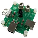
board can be seen in Figure 2 below.
This manual provides a bill of materials, board schematic,
and a layout overview of the evaluation board. The
appropriate setup to evaluate the device is also provided.
This document must be used with the NLAS7222C
datasheet available on www.onsemi.com. The datasheet
contains full technical details about the specifications and
operation of the device. When the intention is to evaluate the
device considering the specifications given in the datasheet,
it is important to take into account the additional circuitry
which may include changes in the characteristic impedance
matching.
Figure 1. Block Diagram of NCN7222C
Figure 2. Evaluation Board
© Semiconductor Components Industries, LLC, 2012
May, 2012 − Rev. 2
1
Publication Order Number:
EVBUM2121/D
�NLAS7222CMUGEVB
TEST PROCEDURE
3. Select the desired output port (HSD1 or HSD2) by
moving the jumpers to the appropriate logic level
for S and OE, as shown in the function table in
Table 1.
4. Connect the USB cable from the desired output
port (HSD1 or HSD2) to the computer’s USB
port. You will now be able to access the USB drive
through the computer.
Equipment
•
•
•
•
•
DC Power Supply
Two Banana Cables
Computer with USB port
USB Flash Drive
USB Cable (Type A to Type B)
Procedure
1. Set the power supply to 3.3 V. Connect the power
supply from VCC to GND using the banana
cables. The supply current should be less than
1 mA.
2. Connect the USB drive to the Common I/O USB
port.
Table 1. FUNCTION TABLE
VCC
OE
S
HSD1+,
HSD1−
HSD2+,
HSD2−
1
0
0
X
0
1
OFF
ON
OFF
OFF
OFF
ON
GND
S and OE/
logic selection
pins
Common
I/O
HSD1
GND connection for
probes
Test point
NLAS7222C
HSD2
Figure 3. Evaluation Board Close−Up
http://onsemi.com
2
�NLAS7222CMUGEVB
SCHEMATIC
Figure 4. Evaluation Board Schematic
http://onsemi.com
3
�NLAS7222CMUGEVB
Table 2. BILL OF MATERIALS
Designator
Qty
Description
Value
Tolerance
Footprint
Manufacturer
Manufacturer Part Number
C1
1
Ceramic Capacitor
SMD
1 mF
10%
0805
AVX
GRM155R60J105
C2
1
Ceramic Capacitor
SMD
0.1 mF
10%
0402
Yageo
CC0402ZRY5V7BB104
J1, J2
2
Banana Connector
n/a
n/a
7 mm
Hole
Johnson
Components
111−2223−001
J3, J4
2
3−Pin Header
n/a
n/a
Header3
Tyco Electronics
5−826629−0
J3, J4
2
2−Pin Jumper
n/a
n/a
n/a
Tyco Electronics
4−881545−2
J5
1
USB TypeA Connector
n/a
n/a
USB
TypeA
Mill−Max
896−43−004−00−000000
J6, J7
2
USB TypeB Connector
n/a
n/a
USB
TypeB
Adam Tech
USB−B−S−RA
J8, J9,
J10, J11
4
Standoff Nut
n/a
n/a
n/a
Keystone
Electronics
1903C
J8, J9,
J10, J11
4
Standoff Screw
n/a
n/a
n/a
Keystone
Electronics
4814K−ND
TP1
1
PCB Shorting Link
n/a
n/a
n/a
Harwin
D3082−46
TP2,
TP3,
TP4,
TP5,
TP6, TP7
6
Test Point PC Multi
Purpose
n/a
n/a
1.6mm
hole
Keystone
Electronics
5010
U1
1
NLAS7222C
n/a
n/a
UQFN10
ON Semiconductor
NLAS7222CMUTBG
http://onsemi.com
4
�NLAS7222CMUGEVB
PCB LAYOUT
The PCB and components are made of lead−free and
RoHS compliant materials. The layout is shown in Figure 5
below. The top layer traces are shown in magenta, and the
bottom layer traces are shown in cyan. Ground pours are
present on the top and bottom layers for connectivity. PCB
dimensions are 53 mm x 58 mm x 1 mm.
Figure 5. Evaluation Board Layout
PCB LAYOUT GUIDELINES
Implementing a high speed USB switch device requires
paying attention on data lines and traces to preserve signal
integrity. The demonstration board serves as layout example
and can support the design engineers to preserve high speed
performances.
Electrical layout guidelines are:
♦ The bypass capacitor must be placed as close as
possible to the VCC input pin for noise immunity.
♦ The characteristics impedance of each switch
segment must be 45 W.
♦
♦
♦
♦
The ground plane of the PCB will be used to
determine the characteristics impedance of each line.
All corresponding D+/D− line segment pairs must
be the same length.
The use of vias to route these signals should be
avoided when possible.
The use of turns or bends to route these signal
should be avoided when possible.
http://onsemi.com
5
�onsemi,
, and other names, marks, and brands are registered and/or common law trademarks of Semiconductor Components Industries, LLC dba “onsemi” or its affiliates
and/or subsidiaries in the United States and/or other countries. onsemi owns the rights to a number of patents, trademarks, copyrights, trade secrets, and other intellectual property. A
listing of onsemi’s product/patent coverage may be accessed at www.onsemi.com/site/pdf/Patent−Marking.pdf. onsemi is an Equal Opportunity/Affirmative Action Employer. This
literature is subject to all applicable copyright laws and is not for resale in any manner.
The evaluation board/kit (research and development board/kit) (hereinafter the “board”) is not a finished product and is not available for sale to consumers. The board is only intended
for research, development, demonstration and evaluation purposes and will only be used in laboratory/development areas by persons with an engineering/technical training and familiar
with the risks associated with handling electrical/mechanical components, systems and subsystems. This person assumes full responsibility/liability for proper and safe handling. Any
other use, resale or redistribution for any other purpose is strictly prohibited.
THE BOARD IS PROVIDED BY ONSEMI TO YOU “AS IS” AND WITHOUT ANY REPRESENTATIONS OR WARRANTIES WHATSOEVER. WITHOUT LIMITING THE FOREGOING,
ONSEMI (AND ITS LICENSORS/SUPPLIERS) HEREBY DISCLAIMS ANY AND ALL REPRESENTATIONS AND WARRANTIES IN RELATION TO THE BOARD, ANY
MODIFICATIONS, OR THIS AGREEMENT, WHETHER EXPRESS, IMPLIED, STATUTORY OR OTHERWISE, INCLUDING WITHOUT LIMITATION ANY AND ALL
REPRESENTATIONS AND WARRANTIES OF MERCHANTABILITY, FITNESS FOR A PARTICULAR PURPOSE, TITLE, NON−INFRINGEMENT, AND THOSE ARISING FROM A
COURSE OF DEALING, TRADE USAGE, TRADE CUSTOM OR TRADE PRACTICE.
onsemi reserves the right to make changes without further notice to any board.
You are responsible for determining whether the board will be suitable for your intended use or application or will achieve your intended results. Prior to using or distributing any systems
that have been evaluated, designed or tested using the board, you agree to test and validate your design to confirm the functionality for your application. Any technical, applications or
design information or advice, quality characterization, reliability data or other services provided by onsemi shall not constitute any representation or warranty by onsemi, and no additional
obligations or liabilities shall arise from onsemi having provided such information or services.
onsemi products including the boards are not designed, intended, or authorized for use in life support systems, or any FDA Class 3 medical devices or medical devices with a similar
or equivalent classification in a foreign jurisdiction, or any devices intended for implantation in the human body. You agree to indemnify, defend and hold harmless onsemi, its directors,
officers, employees, representatives, agents, subsidiaries, affiliates, distributors, and assigns, against any and all liabilities, losses, costs, damages, judgments, and expenses, arising
out of any claim, demand, investigation, lawsuit, regulatory action or cause of action arising out of or associated with any unauthorized use, even if such claim alleges that onsemi was
negligent regarding the design or manufacture of any products and/or the board.
This evaluation board/kit does not fall within the scope of the European Union directives regarding electromagnetic compatibility, restricted substances (RoHS), recycling (WEEE), FCC,
CE or UL, and may not meet the technical requirements of these or other related directives.
FCC WARNING – This evaluation board/kit is intended for use for engineering development, demonstration, or evaluation purposes only and is not considered by onsemi to be a finished
end product fit for general consumer use. It may generate, use, or radiate radio frequency energy and has not been tested for compliance with the limits of computing devices pursuant
to part 15 of FCC rules, which are designed to provide reasonable protection against radio frequency interference. Operation of this equipment may cause interference with radio
communications, in which case the user shall be responsible, at its expense, to take whatever measures may be required to correct this interference.
onsemi does not convey any license under its patent rights nor the rights of others.
LIMITATIONS OF LIABILITY: onsemi shall not be liable for any special, consequential, incidental, indirect or punitive damages, including, but not limited to the costs of requalification,
delay, loss of profits or goodwill, arising out of or in connection with the board, even if onsemi is advised of the possibility of such damages. In no event shall onsemi’s aggregate liability
from any obligation arising out of or in connection with the board, under any theory of liability, exceed the purchase price paid for the board, if any.
The board is provided to you subject to the license and other terms per onsemi’s standard terms and conditions of sale. For more information and documentation, please visit
www.onsemi.com.
PUBLICATION ORDERING INFORMATION
LITERATURE FULFILLMENT:
Email Requests to: orderlit@onsemi.com
onsemi Website: www.onsemi.com
◊
TECHNICAL SUPPORT
North American Technical Support:
Voice Mail: 1 800−282−9855 Toll Free USA/Canada
Phone: 011 421 33 790 2910
www.onsemi.com
1
Europe, Middle East and Africa Technical Support:
Phone: 00421 33 790 2910
For additional information, please contact your local Sales Representative
�


 工商网监
湘ICP备2023018690号
工商网监
湘ICP备2023018690号
