ON Semiconductor
Is Now
To learn more about onsemi™, please visit our website at
www.onsemi.com
onsemi and and other names, marks, and brands are registered and/or common law trademarks of Semiconductor Components Industries, LLC dba “onsemi” or its affiliates and/or
subsidiaries in the United States and/or other countries. onsemi owns the rights to a number of patents, trademarks, copyrights, trade secrets, and other intellectual property. A listing of onsemi
product/patent coverage may be accessed at www.onsemi.com/site/pdf/Patent-Marking.pdf. onsemi reserves the right to make changes at any time to any products or information herein, without
notice. The information herein is provided “as-is” and onsemi makes no warranty, representation or guarantee regarding the accuracy of the information, product features, availability, functionality,
or suitability of its products for any particular purpose, nor does onsemi assume any liability arising out of the application or use of any product or circuit, and specifically disclaims any and all
liability, including without limitation special, consequential or incidental damages. Buyer is responsible for its products and applications using onsemi products, including compliance with all laws,
regulations and safety requirements or standards, regardless of any support or applications information provided by onsemi. “Typical” parameters which may be provided in onsemi data sheets and/
or specifications can and do vary in different applications and actual performance may vary over time. All operating parameters, including “Typicals” must be validated for each customer application
by customer’s technical experts. onsemi does not convey any license under any of its intellectual property rights nor the rights of others. onsemi products are not designed, intended, or authorized
for use as a critical component in life support systems or any FDA Class 3 medical devices or medical devices with a same or similar classification in a foreign jurisdiction or any devices intended for
implantation in the human body. Should Buyer purchase or use onsemi products for any such unintended or unauthorized application, Buyer shall indemnify and hold onsemi and its officers, employees,
subsidiaries, affiliates, and distributors harmless against all claims, costs, damages, and expenses, and reasonable attorney fees arising out of, directly or indirectly, any claim of personal injury or death
associated with such unintended or unauthorized use, even if such claim alleges that onsemi was negligent regarding the design or manufacture of the part. onsemi is an Equal Opportunity/Affirmative
Action Employer. This literature is subject to all applicable copyright laws and is not for resale in any manner. Other names and brands may be claimed as the property of others.
�1-Bit Dual-Supply
Non-Inverting Level
Translator
NLSV1T34
The NLSV1T34 is a 1−bit configurable dual−supply voltage level
translator. The input An and output Bn ports are designed to track two
different power supply rails, VCCA and VCCB respectively. Both
supply rails are configurable from 0.9 V to 4.5 V allowing universal
low−voltage translation from the input An to the output Bn port.
www.onsemi.com
MARKING
DIAGRAMS
•
•
•
•
•
•
•
•
Typical Applications
1
AM
1
QM
1
ULLGA6
MX1 SUFFIX
CASE 613AF
1
Important Information
• ESD Protection for All Pins:
HBM (Human Body Model) > 3000 V
QMG
G
1
PIN ASSIGNMENT
VCCB
VCCA 1
B
A
5
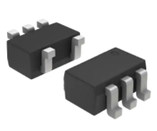
SC−88A
(SOT−353/SC−70)
DF SUFFIX
CASE 419A
Q, A = Device Code
M
= Date Code*
G
= Pb−Free Package
(Note: Microdot may be in either location)
*Date Code orientation and/or position may vary
depending upon manufacturing location.
• Mobile Phones, PDAs, Other Portable Devices
VCCA
M
G
UDFN6
MU SUFFIX
CASE 517AQ
M
•
Wide VCCA and VCCB Operating Range: 0.9 V to 4.5 V
High−Speed w/ Balanced Propagation Delay
Inputs and Outputs have OVT Protection to 4.5 V
Non−preferential VCCA and VCCB Sequencing
Power−Off Protection
Power−Off High Impedance Inputs and Outputs
Ultra−Small Packaging: 1.45 mm x 1.0 mm ULLGA6
2.0 mm x 2.1 mm SC−88A
1.2 mm x 1.0 mm UDFN6
1.45 mm x 1.0 mm UDFN6
NLV Prefix for Automotive and Other Applications Requiring
Unique Site and Control Change Requirements; AEC−Q100
Qualified and PPAP Capable
These are Pb−Free Devices
UDFN6
MU SUFFIX
CASE 517AA
Q
Features
A 2
GND 3
Figure 1. Logic Diagram
6 VCCB VCCA 1
5 NC
4 B
ULLGA6/UDFN6
(Top View)
5 VCCB
A 2
GND 3
4 B
SC−88A
(Top View)
ORDERING INFORMATION
See detailed ordering and shipping information on page 5 of
this data sheet.
© Semiconductor Components Industries, LLC, 2015
November, 2019 − Rev. 10
1
Publication Order Number:
NLSV1T34/D
�NLSV1T34
PIN ASSIGNMENT
TRUTH TABLE
PIN
FUNCTION
INPUTS
OUTPUTS
VCCA
Input Port DC Power Supply
A
B
VCCB
Output Port DC Power Supply
L
L
GND
Ground
H
H
A
Input Port
B
Output Port
MAXIMUM RATINGS
Symbol
VCCA, VCCB
Rating
Value
DC Supply Voltage
VI
DC Input Voltage
VO
DC Output Voltage
IIK
DC Input Diode Current
IOK
IO
Condition
Unit
−0.5 to +5.5
V
A
−0.5 to +5.5
V
(Power Down)
B
−0.5 to +5.5
(Active Mode)
B
−0.5 to +5.5
VCCA = VCCB = 0
V
−20
VI < GND
mA
DC Output Diode Current
−50
VO < GND
mA
DC Output Source/Sink Current
±50
mA
ICCA, ICCB
DC Supply Current Per Supply Pin
±100
mA
IGND
DC Ground Current per Ground Pin
±100
mA
TSTG
Storage Temperature
−65 to +150
°C
V
Stresses exceeding those listed in the Maximum Ratings table may damage the device. If any of these limits are exceeded, device functionality
should not be assumed, damage may occur and reliability may be affected.
RECOMMENDED OPERATING CONDITIONS
Symbol
VCCA, VCCB
VI
VIO
TA
Dt / DV
Parameter
Positive DC Supply Voltage
Bus Input Voltage
Bus Output Voltage
Min
Max
Unit
0.9
4.5
V
GND
4.5
V
(Power Down Mode)
B
GND
4.5
V
(Active Mode)
B
GND
VCCB
V
−40
+85
°C
0
10
nS
Operating Temperature Range
Input Transition Rise or Rate
VI, from 30% to 70% of VCC; VCC = 3.3 V ±0.3 V
Functional operation above the stresses listed in the Recommended Operating Ranges is not implied. Extended exposure to stresses beyond
the Recommended Operating Ranges limits may affect device reliability.
www.onsemi.com
2
�NLSV1T34
DC ELECTRICAL CHARACTERISTICS
−405C to +855C
Symbol
VIH
VIL
VOH
Parameter
Test Conditions
Input HIGH Voltage
Input LOW Voltage
Output HIGH Voltage
VCCA (V)
VCCB (V)
Min
Max
Unit
3.6 – 4.5
0.9 – 4.5
V
2.2
−
2.7 – 3.6
2.0
−
2.3 – 2.7
1.6
−
1.4 − 2.3
0.65 * VCCA
−
0.9 – 1.4
0.9 * VCCA
−
3.6 – 4.5
−
0.8
−
0.8
2.3 – 2.7
−
0.7
1.4 − 2.3
−
0.35 * VCCA
0.9 – 1.4
−
0.1 * VCCA
IOH = −100 mA; VI = VIH
0.9 – 4.5
0.9 – 4.5
VCCB – 0.2
−
IOH = −0.5 mA; VI = VIH
0.9
0.9
0.75 * VCCB
−
IOH = −2 mA; VI = VIH
1.4
1.4
1.05
−
IOH = −6 mA; VI = VIH
1.65
1.65
1.25
−
2.3
2.3
2.0
−
2.3
2.3
1.8
−
2.7
2.7
2.2
−
2.3
2.3
1.7
−
IOH = −12 mA; VI = VIH
IOH = −18 mA; VI = VIH
VOL
Output LOW Voltage
0.9 – 4.5
2.7 – 3.6
3.0
3.0
2.4
−
IOH = −24 mA; VI = VIH
3.0
3.0
2.2
−
IOL = 100 mA; VI = VIL
0.9 – 4.5
0.9 – 4.5
−
0.2
IOL = 0.5 mA; VI = VIH
1.1
1.1
−
0.3
IOL = 2 mA; VI = VIH
1.4
1.4
−
0.35
IOL = 6 mA; VI = VIL
1.65
1.65
−
0.3
IOL = 12 mA; VI = VIL
2.3
2.3
−
0.4
2.7
2.7
−
0.4
2.3
2.3
−
0.6
3.0
3.0
−
0.4
IOL = 18 mA; VI = VIL
IOL = 24 mA; VI = VIL
V
V
V
3.0
3.0
−
0.55
Input Leakage Current
VI = VCCA or GND
0.9 – 4.5
0.9 – 4.5
−1.0
1.0
mA
ICCA
Quiescent Supply Current
VI = VCCA or GND;
IO = 0, VCCA = VCCB
0.9 – 4.5
0.9 − 4.5
−
2.0
mA
ICCB
Quiescent Supply Current
VI = VCCA or GND;
IO = 0, VCCA = VCCB
0.9 – 4.5
0.9 − 4.5
−
2.0
mA
ICCA + ICCB Quiescent Supply Current
VI = VCCA or GND;
IO = 0, VCCA = VCCB
0.9 – 4.5
0.9 – 4.5
−
4.0
mA
0
0
−
5.0
mA
II
IOFF
Power OFF Leakage Current
VI = 4.5 V
Product parametric performance is indicated in the Electrical Characteristics for the listed test conditions, unless otherwise noted. Product
performance may not be indicated by the Electrical Characteristics if operated under different conditions.
www.onsemi.com
3
�NLSV1T34
TOTAL STATIC POWER CONSUMPTION (ICCA + ICCB)
−405C to +855C
VCCB (V)
4.5
VCCA (V)
Min
3.3
Max
Min
2.8
Max
Min
1.8
Max
Min
0.9
Max
Min
Max
Unit
4.5
2
2
2
2
< 1.5
μA
3.3
2
2
2
2
< 1.5
μA
2.8


 工商网监
湘ICP备2023018690号
工商网监
湘ICP备2023018690号

