NOA1302 Ambient Light Sensor with I2C Interface
Description
The NOA1302 integrates a wide dynamic range ambient light sensor (ALS) with a 16−bit ADC and a 2−wire I2C digital interface. The NOA1302 ambient light sensor provides a linear response over the range of close to 0 lux to well over 100,000 lux with programmable integration times to optimize noise performance. The sensor employs proprietary CMOS image sensing technology from ON Semiconductor which provides low noise and high dynamic range output signals and light response similar to the response of the human eye. The NOA1302 operates as an I2C slave device and supports commands to set options in the device and read out the ambient light intensity count.
Features
http://onsemi.com
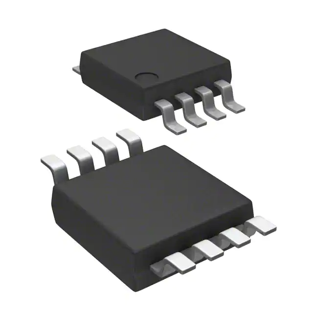
CTSSOP−8 DC SUFFIX CASE 949AA
MARKING DIAGRAM
8 1302
• Senses Ambient Light and Provides an Output Count Proportional to • Human Eye Type of Spectral Response • Provides Comfortable Levels of Display Depending on the Viewing • • • • • • • •
the Ambient Light Intensity
(Top View)
Applications
• Saves Display Power in Applications such as:
− Laptops, Notebooks, Digital Signage − LCD TVs and Monitors, Digital Picture Frames − LED Indoor/Outdoor Residential and Street Lights
Vin = 3.3 V hv 6 VDD SDA 5 SCL 4 R1 1k R2 1k SDA MCU SCL
ORDERING INFORMATION
See detailed ordering and shipping information in the package dimensions section on page 2 of this data sheet.
C1 10m
C2 0.1m
3 VSS
IC1 NOA1302
CL not to exceed 250 pF including all parasitic capacitances
Figure 1. Typical Application Circuit
© Semiconductor Components Industries, LLC, 2009
August, 2009 − Rev. 1
1
ÉÉ ÉÉ
Environment Linear Response Over the Full Operating Range Senses Intensity of Ambient Light from ~0 Lux to over 100,000 Lux Programmable Integration Times of 400 ms, 200 ms and 100 ms No External Components Required Low Power Consumption Built−in 16−bit ADC I2C Serial Communication Port − Standard Mode – 100 kHz − Fast Mode – 400 kHz This Device is Pb−Free, Halogen Free/BFR Free, and RoHS Compliant
1
1302= Specific Device Code A = Assembly Location Y = Year W = Work Week G = Pb−Free Package
PIN ASSIGNMENT
NC NC VSS SCL 1 8 NC NC VDD SDA
ÉÉ ÉÉ
AYWG
Publication Order Number: NOA1302/D
�NOA1302
Table 1. ORDERING INFORMATION
Part Number NOA1302DCRG Package CTSSOP−8 (Pb−Free) Shipping Configuration† 2500 / Tape & Reel Temperature Range 0°C to 70°C
†For information on tape and reel specifications, including part orientation and tape sizes, please refer to our Tape and Reel Packaging Specification Brochure, BRD8011/D. ADC
hn
16−bits Control SCL SDA
I2C Serial Interface
Figure 2. Simplified Block Diagram
Table 2. PIN FUNCTION DESCRIPTION
Pin 1, 2, 7, 8 3 4 5 6 Pin Name N/C VSS SCL SDA VDD Not connected, leave this pin unconnected. Ground pin. External I2C clock supplied by the I2C master. Bi−directional data signal for communications between this device and the I2C master. Power pin. Description
Table 3. ABSOLUTE MAXIMUM RATINGS
Rating Input power supply Input voltage range Output voltage range Maximum Junction Temperature Storage Temperature ESD Capability, Human Body Model (Note 1) ESD Capability, Charged Device Model (Note 1) ESD Capability, Machine Model (Note 1) Moisture Sensitivity Level Lead Temperature Soldering (Note 2) Symbol VDD Vin Vout TJ(max) TSTG ESDHBM ESDCDM ESDMM MSL TSLD Value 5.5 −0.3 to VDD + 0.2 −0.3 to VDD + 0.2 85 −40 to 85 2.5 750 250 3 260 Unit V V V °C °C kV V V − °C
Stresses exceeding Maximum Ratings may damage the device. Maximum Ratings are stress ratings only. Functional operation above the Recommended Operating Conditions is not implied. Extended exposure to stresses above the Recommended Operating Conditions may affect device reliability. 1. This device incorporates ESD protection and is tested by the following methods: ESD Human Body Model tested per EIA/JESD22−A114 ESD Charged Device Model tested per ESD−STM5.3.1−1999 ESD Machine Model tested per EIA/JESD22−A115 Latchup Current Maximum Rating: ≤ 100 mA per JEDEC standard: JESD78 2. For information, please refer to our Soldering and Mounting Techniques Reference Manual, SOLDERRM/D
http://onsemi.com
2
�NOA1302
Table 4. OPERATING RANGES
Standard Mode Rating Power supply voltage Power supply current (VDD = 3.3 V) Low level input voltage (VDD related input levels) High level input voltage (VDD related input levels) Hysteresis of Schmitt trigger inputs (VDD > 2 V) Low level output voltage (open drain) at 3 mA sink current (VDD > 2 V) High level output voltage (with 1 kW pullup resistance) at and output current of −20 mA (VDD > 2 V) Input current of IO pin with an input voltage between 0.1 VDD and 0.9 VDD Output low current Capacitance on IO pin Operating free−air temperature range Symbol VDD IDD VIL VIH Vhys VOL VOH II IOL CI TA Min 3.0 325 −0.3 0.7 VDD N/A 0 VDD − 0.1 −10 − − 0 Max 3.6 950 0.3 VDD VDD + 0.2 N/A 0.4 N/A 10 45 10 70 Min 3.0 325 −0.3 0.7 VDD 0.05 VDD 0 VDD − 0.1 −10 − − 0 Fast Mode Max 3.6 950 0.3 VDD VDD + 0.2 − 0.4 N/A 10 45 10 70 Unit V mA V V V V V mA mA pF °C
Table 5. ELECTRICAL CHARACTERISTICS
(Unless otherwise specified, these specifications apply over VDD = 3.3 V, 0°C < TA < 70°C) (Note 3) Standard Mode Parameter SCL clock frequency Hold time for START condition. After this period, the first clock pulse is generated. Low period of SCL clock High period of SCL clock Data hold time for I2C−bus devices Data set−up time Rise time of both SDA and SCL (input signals) (Note 4) Fall time of both SDA and SCL (input signals) (Note 4) Rise time of SDA output signal (Note 4) Fall time of SDA output signal (Note 4) Output fall time from VIHmin to VILmax with a bus capacitance from 10 pF to 250 pF. (Note 5) Set−up time for STOP condition Bus free time between STOP and START condition Capacitive load for each bus line (including all parasitic capacitance) Noise margin at the low level for each connected device (including hysteresis) Noise margin at the high level for each connected device (including hysteresis) Symbol fSCL tHD;STA tLOW tHIGH tHD;DAT_d tSU;DAT tr_INPUT tf_INPUT tr_OUT tf_OUT tof tSU;STO tBUF CL VnL VnH Min 10 4.0 4.7 4.0 0 250 5 5 − − 2 4.0 4.7 − 0.1 VDD 0.2 VDD 3.45 − 300 300 1000 1000 250 − − 250 − − Max 100 − Fast Mode Min 100 0.6 1.3 0.6 0 100 5 5 − − 2 0.6 1.3 − 0.1 VDD 0.2 VDD 0.9 − 300 300 1000 1000 250 − − 250 − − Max 400 − Unit kHz mS mS mS mS nS nS nS nS nS nS mS mS pF V V
3. Refer to Figure 3 for more information on AC characteristics 4. The rise time and fall time are measured with a pull−up resistor Rp = 1 kW and Cb of 250 pF (including all parasitic capacitances). 5. Cb = capacitance of one bus line, maximum value of which including all parasitic capacitances should be less than 250 pF.
http://onsemi.com
3
�NOA1302
Table 6. OPTICAL CHARACTERISTICS (Unless otherwise specified, these specifications are for VDD = 3.3 V, TA = 25°C)
Parameter Irradiance responsivity Illuminance responsivity Test Conditions lp (see Figure 5) Incandescent light source: Ev = 100 lux (see Figure 6) Incandescent light source: Ev = 1000 lux (see Figure 6) Illuminance responsivity Fluorescent light source: Ev = 100 lux (see Figure 7) Fluorescent light source: Ev = 1000 lux (see Figure 7) Dark current Ev = 0 lux (see Figure 9) Rv Symbol Re Rv Min Typ 545 150 1480 130 1290 2 Counts Counts Max Unit nM Counts
SDA tf tLOW tr tSU;DAT tf tSP tr tBUF
SCL S tHD;STA tHD;DAT tHIGH tSU;STO P S
Figure 3. AC Characteristics
http://onsemi.com
4
�NOA1302
TYPICAL CHARACTERISTICS
Figure 4. Photo Diode Spectral Response (Without Filter)
Figure 5. Human Eye vs. NOA1302 Spectral Response
Figure 6. Incandescent Light Response (200 ms Integration)
Figure 7. Fluorescent Light Response (200 ms Integration)
Figure 8. Light Response vs. VDD
Figure 9. Dark Counts vs. Temperature (200 ms Integration)
http://onsemi.com
5
�NOA1302
TYPICAL CHARACTERISTICS
Figure 10. Dark Counts vs. Vdd
Figure 11. Idd vs. Temperature
Figure 12. Idd vs.Vdd
Figure 13. Idd vs Ev
Figure 14. Maximum Value of RP (in kW) as a function of Bus Capacitance (in pF)
http://onsemi.com
6
�NOA1302
DESCRIPTION OF OPERATION
Ambient Light Sensor Architecture
The NOA1302 employs a sensitive photo diode fabricated in ON Semiconductor’s standard CMOS process technology. The major components of this sensor are as shown in Figure 2. The photons which are to be detected pass through an ON Semiconductor proprietary color filter limiting extraneous photons and thus performing as a band pass filter on the incident wave front. The filter only transmits photons in the visible spectrum which are primarily detected by the human eye. The photo response of this sensor is as shown in Figure 5. The ambient light signal detected by the photo diode is converted to digital signal using a variable slope integrating ADC with a resolution of 16−bits, unsigned. The ADC value is provided to the control block connected to the I2C interface block. Equation 1 shows the relationship of output counts Cnt as a function of integration constant Ik, integration time Tint (in seconds) and the intensity of the ambient light, IL(in lux), at room temperature (25°C).
IL + C nt (I k @ T int)
(eq. 1)
sent MSB first. RD/WR_ command bit follows the address bits. Upon receiving a valid address the device responds by driving SDA low for an ACK. After receiving an ACK, the I2C master sends eight bits of data with MSB first. Upon receiving eight bits of data the NOA1302 generates an ACK. The I2C master terminates this write command with a stop condition.
SDA A[6:0] WR ACK D[7:0] ACK
SCL Start Condition Stop Condition
Figure 15. I2C Write Command
Where: Ik = 6.67 (for fluorescent light) Ik = 7.5 (for incandescent light) Hence the intensity of the ambient fluorescent light (in lux):
IL + C nt (6.67 @ T int) C nt (7.5 @ T int)
(eq. 2)
and the intensity of the ambient incandescent light (in lux):
IL +
(eq. 3)
Figure 16 shows an I2C read command sent by the master to the slave device. The I2C read command begins with a start condition. After the start condition, seven bits of address are sent by the master MSB first, followed by the RD/WR_ command bit. For a read command the RD/WR_ bit is high. Upon receiving the address bits and RD/WR_ command bits the device responds with an ACK. After sending an ACK, the device sends eight bits of data MSB first. After receiving the data, the master terminates this transaction by issuing a NACK command to indicate that the master only wanted to read one byte from the device. The master generates a stop condition to end this transaction. Repeated START condition is not supported. Each I2C transaction must be terminated with a STOP condition after all required bits have been transmitted and received.
For example let: Cnt = 1200 Tint = 200 mS Intensity of ambient incandescent light, IL(in lux):
1200 IL + (7.5 @ 200 mS)
(eq. 4)
SDA
A[6:0]
RD
ACK
D[7:0] NACK
SCL Start Condition Stop Condition
IL = 800 lux The NOA1302 operates on the I2C bus as a slave device. The I2C address is fixed at 0x39 (hexadecimal 39). Registers can be programmed by sending commands over an I2C bus. Ambient light intensity count value can be obtained by reading registers. The ambient light intensity count is 16 bits, hence two I2C read operations are needed. This device supports both standard (100 Kbit/s) and fast mode (400 Kbit/s) of operation on the I2C bus. Figure 15 shows an I2C write operation. To write to an internal register of the NOA1302 a write command must be sent by an I2C master. The write command begins with a start condition. After the start condition, seven bits of address are
I2C Interface
Figure 16. I2C Read Command Programmer’s Model
Ambient light intensity count is obtained from the the NOA1302 by issuing a fixed sequence of I2C commands. Integration time is programmable by writing different values to the integration time register. The following sections describe what a programmer needs to know about issuing commands to the chip and register access.
Integration Time Register
Table 7 describes integration time register which controls the exposure time. This register has three bits, EC[2:0] which control the duration of the integration time.
http://onsemi.com
7
�NOA1302
Table 7. INTEGRATION TIME REGISTER
EC[2,1,0] 000 001 010 011 100 101 110 111 Operation Normal mode of operation Normal mode of operation Normal mode of operation Test mode Simulation test mode use only Reserved for future use Reserved for future use Reserved for future use Integration Time 400 ms 200 ms (Default) 100 ms 16.7 ms 1.0 ms
1. Send write command 0x1Dh to set EC[0] = 0. 2. Send write command 0x88h to set EC[1] = 1, now EC[2:0] = 010. Proper operation of the I2C bus depends on keeping the bus capacitance low and selecting suitable pull−up resistor values. Figure 17 and Figure 18 show the rise and fall time on SDA in output mode under maximum load conditions. The measurement set−up is shown in Figure 19. Figure 14 shows the maximum value of the pull−up resistor (RP) as a function of the I2C data bus capacitance.
Rise and Fall Time of SDA (Output)
Programming Sequence and Command Summary
This section describes supported commands and programming sequence. The NOA1302 only supports single byte write and a single byte read I2C commands. Ambient light intensity count is 16 bits wide, thus two I2C read commands are needed. Table 8 describes supported commands. All of these commands have to be sent to the fixed address (0x39).
Table 8. DEVICE COMMANDS
Command 0x00h 0x03h 0x1Dh 0x18h 0x43h 0x83h 0x88h 0x90h Function Start reading ADC data Complete reading ADC data Change EC[0] to 0 Reset EC[2:0] to default value (001) Prepare ADC LS byte for reading Prepare ADC MS byte for reading Change EC[1] to 1 Change EC[2] to 1 RP = 1 kW CL = 250 pF (including all parasitic caps) tr = 530 ns
Figure 17. SDA Rise Time (tr)
Programming Sequence
To read 16 bits wide ambient light intensity count, the following commands must be issued in sequence: 1. Send write command 0x00h to start the ADC conversion cycle. 2. Send write command 0x03h to complete the ADC cycle. 3. Send write command 0x43h to prepare the LS byte for reading. 4. Send read byte command, returns LS byte of count. 5. Send write command 0x83h to prepare the MS byte for reading. 6. Send read byte command, returns MS byte of count. To change the integration time, for example to 100 ms, the following commands must be used in sequence:
RP = 1 kW CL = 250 pF (including all parasitic caps) tf = 21 ns
Figure 18. SDA Fall Time (tf)
16−bits Control I2C Serial Interface SCL SDA
LED Pulse Generator
hn
ADC
NOA1302
Figure 19. Measurement Set−up
http://onsemi.com
8
�NOA1302
PACKAGE DIMENSIONS
CTSSOP8 3x3 CASE 949AA−01 ISSUE O
0.20 C D A
8 5 NOTE 5
4X
D
8X b
D2
0.15
NOTE 3
M
C A-B D
E2 E1
PIN 1 INDICATOR NOTE 6
E 0.25
1 4
NOTES: 1. DIMENSIONING AND TOLERANCING PER ASME Y14.5M, 1994. 2. CONTROLLING DIMENSION: MILLIMETER. 3. DIMENSION b DOES NOT INCLUDE DAMBAR PROTRUSION AND IS DETERMINED BETWEEN 0.08 AND 0.15 MM FROM THE LEAD TIP. 4. DIMENSIONS D AND E1 DOES NOT INCLUDE MOLD PROTRUSIONS, TIE BAR BURRS, GATE BURRS OR FLASH. END FLASH SHALL NOT EXCEED 0.25 PER SIDE. DIMENSIONS D AND E1 DO INCLUDE ANY MOLD CAVITY MISMATCH AND ARE DETERMINED AT THE GAUGE PLANE. 5. DATUMS A AND B TO BE DETERMINED AT THE GAUGE PLANE. 6. DETAILS OF THE PIN 1 IDENTIFIER ARE OPTIONAL, BUT MUST BE LOCATED WITHIN THIS ZONE. DIM A A1 A2 b c D D2 E E1 E2 e L M MILLIMETERS MIN MAX −−− 1.10 0.00 0.14 0.73 0.93 0.24 0.39 0.13 0.24 3.00 BSC 0.66 1.37 4.90 BSC 3.00 BSC 0.41 1.37 0.65 BSC 0.39 0.67 0° 8°
B
NOTE 5
e
TOP VIEW
e/2 AUXILIARY TOP VIEW
C
M
L DETAIL A
GAUGE PLANE
A A1 A2 SIDE VIEW C
8X
DETAIL A
0.15 C
SEATING PLANE
c
END VIEW
SOLDERING FOOTPRINT*
0.48
8X
0.72
8X
1.05
0.65 PITCH
DIMENSIONS: MILLIMETERS
*For additional information on our Pb−Free strategy and soldering details, please download the ON Semiconductor Soldering and Mounting Techniques Reference Manual, SOLDERRM/D.
ON Semiconductor and are registered trademarks of Semiconductor Components Industries, LLC (SCILLC). SCILLC reserves the right to make changes without further notice to any products herein. SCILLC makes no warranty, representation or guarantee regarding the suitability of its products for any particular purpose, nor does SCILLC assume any liability arising out of the application or use of any product or circuit, and specifically disclaims any and all liability, including without limitation special, consequential or incidental damages. “Typical” parameters which may be provided in SCILLC data sheets and/or specifications can and do vary in different applications and actual performance may vary over time. All operating parameters, including “Typicals” must be validated for each customer application by customer’s technical experts. SCILLC does not convey any license under its patent rights nor the rights of others. SCILLC products are not designed, intended, or authorized for use as components in systems intended for surgical implant into the body, or other applications intended to support or sustain life, or for any other application in which the failure of the SCILLC product could create a situation where personal injury or death may occur. Should Buyer purchase or use SCILLC products for any such unintended or unauthorized application, Buyer shall indemnify and hold SCILLC and its officers, employees, subsidiaries, affiliates, and distributors harmless against all claims, costs, damages, and expenses, and reasonable attorney fees arising out of, directly or indirectly, any claim of personal injury or death associated with such unintended or unauthorized use, even if such claim alleges that SCILLC was negligent regarding the design or manufacture of the part. SCILLC is an Equal Opportunity/Affirmative Action Employer. This literature is subject to all applicable copyright laws and is not for resale in any manner.
PUBLICATION ORDERING INFORMATION
LITERATURE FULFILLMENT: Literature Distribution Center for ON Semiconductor P.O. Box 5163, Denver, Colorado 80217 USA Phone: 303−675−2175 or 800−344−3860 Toll Free USA/Canada Fax: 303−675−2176 or 800−344−3867 Toll Free USA/Canada Email: orderlit@onsemi.com N. American Technical Support: 800−282−9855 Toll Free USA/Canada Europe, Middle East and Africa Technical Support: Phone: 421 33 790 2910 Japan Customer Focus Center Phone: 81−3−5773−3850 ON Semiconductor Website: www.onsemi.com Order Literature: http://www.onsemi.com/orderlit For additional information, please contact your local Sales Representative
http://onsemi.com
9
NOA1302/D
�


 工商网监
湘ICP备2023018690号
工商网监
湘ICP备2023018690号
