NCV890201GEVB
NCV890201 Automotive
Grade High-Frequency
Buck Regulator Evaluation
Board User's Manual
http://onsemi.com
Description
The NCV890201 demonstration board provides a convenient way to
evaluate a high-frequency buck converter design. No additional
components are required, other than dc supplies for the input and
enable voltages. An external clock can be used to synchronize the
switching frequency; and the board also provides a synchronization
output, enabling it to be used as a master. It is configured for a 3.3 V
output with a 2 MHz switching frequency and a 2.0 A maximum
output current, over the typical 4.5 V to 18 V automotive input voltage
range. In addition, the board regulates up to 36 V thanks to switching
frequency foldback.
EVAL BOARD USER’S MANUAL
Key Features
•
•
•
•
•
•
•
•
3.3 V Output Voltage
2 MHz Switching Frequency
2.0 A Current Limit
Wide Input Voltage of 4.5 V to 36 V
Regulates through Load Dump Conditions
External Clock Synchronization up to 2.5 MHz
Synchronization Output
Automotive Grade
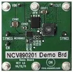
Figure 1. NCV890201GEVB Board Picture
© Semiconductor Components Industries, LLC, 2011
December, 2011 − Rev. P1
1
Publication Order Number:
EVBUM2050/D
�NCV890201GEVB
Table 1. DEMONSTRATION BOARD TERMINALS
Terminal
Function
VIN
Positive dc input voltage
GND
Common dc return
VOUT
Regulated dc output voltage
EN
Enable input
SYNCI
Input for external clock synchronization
SYNCO
Output for synchronizing other boards
Table 2. ABSOLUTE MAXIMUM RATINGS
(Voltages are with respect to GND)
Value
Units
Dc supply voltage (VIN, EN)
-0.3 to 36 V
V
Dc supply voltage (SYNCI)
-0.3 to 6 V
V
Junction Temperature (NCV890201)
-40 to 150
°C
Ambient temperature (Demo Board)
-40 to 85
°C
Rating
Stresses exceeding Maximum Ratings may damage the device. Maximum Ratings are stress ratings only. Functional operation
above the Recommended Operating Conditions is not implied. Extended exposure to stresses above the Recommended
Operating Conditions may affect device reliability.
Table 3. ELECTRICAL CHARACTERISTICS
(TA = 25°C, 4.5 V ≤ VIN ≤ 40 V, VEN = 2 V, VOUT = 3.3 V, 0 ≤ IOUT ≤ 2.0 A, unless otherwise specified)
Characteristics
Conditions
Typical Value
Units
3.30
V
4
%
Regulation
Output Voltage
Voltage Accuracy
Line Regulation
IOUT = 1.0 A
0.12
%
Load Regulation
VIN = 13.2 V
0.03
%
Switching Frequency
2.0
MHz
Soft-start Time
1.4
ms
1.8 to 2.5
MHz
1.8
A
2.45
A
VIN decreasing
4.2
V
TA increasing
170
°C
Switching
SYNCI Frequency range
Current Limit
Average Current Limit
VIN = 6 to 18 V
Cycle-by-cycle Current Limit
Protections
Input Undervoltage Lockout (UVLO)
Thermal Shutdown
http://onsemi.com
2
�NCV890201GEVB
Figure 2. NCV890201GEVB Board Schematic
Operational Guidelines
1. Connect a dc input voltage, within the 4.5 V to 36 V range, between VIN and GND
2. Connect a load between VOUT and GND
3. Connect a dc enable voltage, within the 4.5 V to 36 V range, between EN and GND
4. Optionally, for external clock synchronization, connect a pulse source between SYNCI and GND. The high state level
should be within the 2 to 6 V range, and the low state level within the -0.3 V to 0.8 V range, with a minimum pulse
width of 40 ns and a frequency within the 1.8 to 2.5 MHz range.
IOUT
ZOUT
VIN
VSYNCI
VEN
Figure 3. NCV890201GEVB Board Connections
http://onsemi.com
3
�NCV890201GEVB
TYPICAL PERFORMANCE
Efficiency
Figure 4. Efficiency at 2 MHz for a 3.3 V output
Start−up
Figure 5. Typical start−up with VIN = 13.2 V,
VOUT = 3.3 V and IOUT = 0.2 A
Figure 6. Typical start−up with VIN = 13.2 V,
VOUT = 3.3 V and IOUT = 1.8 A
http://onsemi.com
4
�NCV890201GEVB
Load Transients
Figure 7. Load transient 0.1 A to 2.0 A,
with VOUT = 3.3 V and VIN = 13.2 V
Figure 8. Load transient 0.2 A to 2.0 A,
with VOUT = 3.3 V and VIN = 13.2 V
Figure 9. Load transient 2.0 A to 0.2 A,
with VOUT = 3.3 V and VIN = 13.2 V
http://onsemi.com
5
�NCV890201GEVB
Synchronization
SYNCI
SYNCO
SW
VOUT
Figure 10. Starting synchronization at 2.5 MHz (from free−running)
Minimum on time
VOUT
VIN
80 ns
SW
Figure 11. Minimum on time seen during a load transient
http://onsemi.com
6
�NCV890201GEVB
Schematic
http://onsemi.com
7
�NCV890201GEVB
PCB LAYOUT
Figure 12. Top View
Figure 13. Bottom View
http://onsemi.com
8
�NCV890201GEVB
Table 4. BILL OF MATERIALS
Reference
Value
Part #
Manufacturer
Description
Package
NCV890201
ON Semiconductor
Integrated circuit
3x3 DFN10
7447786004
Wurth
Inductor
WE-PD-XS
DFW
MBR340MFS
ON Semiconductor
Diode, Schottky, 1.5A, 40V
SMB
DBST
BAS16HT1
ON Semiconductor
Diode, Switching, 200mA, 75V
SOD-323
4.7 mF
Murata
Capacitor, Ceramic, 50V, X7R
1210
U1
L1
CVIN1
4.7 mH
CVIN2
1 mF
Murata
Capacitor, Ceramic, 50V, X5R
0805
CDRV, CBST
0.1 mF
Kemet
Capacitor, Ceramic, 10V, X7R
0603
ZFB1
4.7 nF
Murata
Capacitor, Ceramic, 50V, X7R
0603
COUT1, COUT2
10 mF
Murata
Capacitor, Ceramic, 10V, X7R
1206
CCOMP
330 pF
Murata
Capacitor, Ceramic, 50V, C0G
0603
RCOMP
12.4 KW
Vishay
Resistor, 1%
0603
RFB1
100 W
Vishay
Resistor, 1%
0603
RFB2
31.6 W
Vishay
Resistor, 1%
0603
http://onsemi.com
9
�onsemi,
, and other names, marks, and brands are registered and/or common law trademarks of Semiconductor Components Industries, LLC dba “onsemi” or its affiliates
and/or subsidiaries in the United States and/or other countries. onsemi owns the rights to a number of patents, trademarks, copyrights, trade secrets, and other intellectual property. A
listing of onsemi’s product/patent coverage may be accessed at www.onsemi.com/site/pdf/Patent−Marking.pdf. onsemi is an Equal Opportunity/Affirmative Action Employer. This
literature is subject to all applicable copyright laws and is not for resale in any manner.
The evaluation board/kit (research and development board/kit) (hereinafter the “board”) is not a finished product and is not available for sale to consumers. The board is only intended
for research, development, demonstration and evaluation purposes and will only be used in laboratory/development areas by persons with an engineering/technical training and familiar
with the risks associated with handling electrical/mechanical components, systems and subsystems. This person assumes full responsibility/liability for proper and safe handling. Any
other use, resale or redistribution for any other purpose is strictly prohibited.
THE BOARD IS PROVIDED BY ONSEMI TO YOU “AS IS” AND WITHOUT ANY REPRESENTATIONS OR WARRANTIES WHATSOEVER. WITHOUT LIMITING THE FOREGOING,
ONSEMI (AND ITS LICENSORS/SUPPLIERS) HEREBY DISCLAIMS ANY AND ALL REPRESENTATIONS AND WARRANTIES IN RELATION TO THE BOARD, ANY
MODIFICATIONS, OR THIS AGREEMENT, WHETHER EXPRESS, IMPLIED, STATUTORY OR OTHERWISE, INCLUDING WITHOUT LIMITATION ANY AND ALL
REPRESENTATIONS AND WARRANTIES OF MERCHANTABILITY, FITNESS FOR A PARTICULAR PURPOSE, TITLE, NON−INFRINGEMENT, AND THOSE ARISING FROM A
COURSE OF DEALING, TRADE USAGE, TRADE CUSTOM OR TRADE PRACTICE.
onsemi reserves the right to make changes without further notice to any board.
You are responsible for determining whether the board will be suitable for your intended use or application or will achieve your intended results. Prior to using or distributing any systems
that have been evaluated, designed or tested using the board, you agree to test and validate your design to confirm the functionality for your application. Any technical, applications or
design information or advice, quality characterization, reliability data or other services provided by onsemi shall not constitute any representation or warranty by onsemi, and no additional
obligations or liabilities shall arise from onsemi having provided such information or services.
onsemi products including the boards are not designed, intended, or authorized for use in life support systems, or any FDA Class 3 medical devices or medical devices with a similar
or equivalent classification in a foreign jurisdiction, or any devices intended for implantation in the human body. You agree to indemnify, defend and hold harmless onsemi, its directors,
officers, employees, representatives, agents, subsidiaries, affiliates, distributors, and assigns, against any and all liabilities, losses, costs, damages, judgments, and expenses, arising
out of any claim, demand, investigation, lawsuit, regulatory action or cause of action arising out of or associated with any unauthorized use, even if such claim alleges that onsemi was
negligent regarding the design or manufacture of any products and/or the board.
This evaluation board/kit does not fall within the scope of the European Union directives regarding electromagnetic compatibility, restricted substances (RoHS), recycling (WEEE), FCC,
CE or UL, and may not meet the technical requirements of these or other related directives.
FCC WARNING – This evaluation board/kit is intended for use for engineering development, demonstration, or evaluation purposes only and is not considered by onsemi to be a finished
end product fit for general consumer use. It may generate, use, or radiate radio frequency energy and has not been tested for compliance with the limits of computing devices pursuant
to part 15 of FCC rules, which are designed to provide reasonable protection against radio frequency interference. Operation of this equipment may cause interference with radio
communications, in which case the user shall be responsible, at its expense, to take whatever measures may be required to correct this interference.
onsemi does not convey any license under its patent rights nor the rights of others.
LIMITATIONS OF LIABILITY: onsemi shall not be liable for any special, consequential, incidental, indirect or punitive damages, including, but not limited to the costs of requalification,
delay, loss of profits or goodwill, arising out of or in connection with the board, even if onsemi is advised of the possibility of such damages. In no event shall onsemi’s aggregate liability
from any obligation arising out of or in connection with the board, under any theory of liability, exceed the purchase price paid for the board, if any.
The board is provided to you subject to the license and other terms per onsemi’s standard terms and conditions of sale. For more information and documentation, please visit
www.onsemi.com.
PUBLICATION ORDERING INFORMATION
LITERATURE FULFILLMENT:
Email Requests to: orderlit@onsemi.com
onsemi Website: www.onsemi.com
◊
TECHNICAL SUPPORT
North American Technical Support:
Voice Mail: 1 800−282−9855 Toll Free USA/Canada
Phone: 011 421 33 790 2910
www.onsemi.com
1
Europe, Middle East and Africa Technical Support:
Phone: 00421 33 790 2910
For additional information, please contact your local Sales Representative
�