PCS3PS550A General Purpose Peak EMI Reduction IC
Product Description
The PCS3PS550A is a versatile 2.3 V to 3.6 V, Timing−Safe™, spectrum frequency modulator designed specifically for a wide range of clock frequencies. The PCS3PS550A reduces electromagnetic interference (EMI) at the clock source, allowing system wide reduction of EMI of all clock dependent signals. The PCS3PS550A allows significant system cost savings by reducing the number of circuit board layers ferrite beads, shielding that are traditionally required to pass EMI regulations.
Features
http://onsemi.com MARKING DIAGRAMS
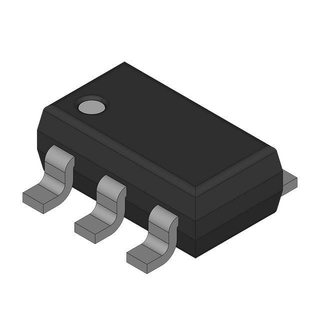
1 WDFN8 CASE 511AQ 1
CAMG G
• • • • • • • •
LVCMOS Peak EMI reduction IC Input Clock Frequency: 18 MHz − 36 MHz Output Clock Frequency: 18 MHz − 36 MHz Eight different selectable Spread options Power Down option for power save Supply Voltage: 2.3 V − 3.6 V 8−pin WDFN , 2 mm x 2 mm (TDFN) Package These Devices are Pb−Free, Halogen Free/BFR Free and are RoHS Compliant
CA = Specific Device Code M = Date Code G = Pb−Free Device
PIN CONFIGURATION
CLKIN SR2 PD# VSS 1 2 3 4 8 7 6 5 VDD SR0 SR1 ModOUT
Applications
• The PCS3PS550A is targeted towards consumer electronic
applications.
PCS3PS550A
ORDERING INFORMATION
See detailed ordering and shipping information in the package dimensions section on page 6 of this data sheet.
© Semiconductor Components Industries, LLC, 2010
July, 2010 − Rev. 1
1
Publication Order Number: PCS3PS550A/D
�PCS3PS550A
VDD
SR0
SR1
SR2
CLKIN
ModOUT PLL
VSS
PD#
Figure 1. Block Diagram
PCS3PS550A modulates the output of a single PLL in order to “spread” the bandwidth of a synthesized clock, and more importantly, decreases the peak amplitudes of its harmonics. This results in significantly lower system EMI compared to the typical narrow band signal produced by oscillators and most frequency generators. Lowering EMI by increasing a signal’s bandwidth is called ‘spread spectrum clock generation’.
Table 1. PIN DESCRIPTION
Pin# 1 2 3 Pin Name CLKIN SR2 PD# Type I I I
PCS3PS550A accepts an input from an external reference clock and locks to a 1x modulated clock output. SR0, SR1 and SR2 pins enable selecting one of the eight different frequency deviations (Refer Frequency Deviation Selection table). PCS3PS550A also features power down option for power save. PCS3PS550A operates over a supply voltage range of 2.3 V to 3.6 V. PCS3PS550A is available in an 8 Pin WDFN, (2 mm x 2 mm) Package.
Description External reference clock input. Digital logic input used to select Spreading Range. There is NO default state. Refer Frequency Deviation Selection Table. Power−down control pin. Powers down the entire chip. There is NO default state. Pull low to enable power−down mode. Connect to VDD to disable Power Down. Output Clock will be LOW when power down is enabled Ground connection. Spread Spectrum Clock Output. Digital logic input used to select Spreading Range. This pin has an internal pull−up resistor. Refer Modulation Selection Table. Digital logic input used to select Spreading Range. There is NO default state. Refer Frequency Deviation Selection Table. Power supply for the entire chip
4 5 6 7 8
VSS ModOUT SR1 SR0 VDD
P O I I P
http://onsemi.com
2
�PCS3PS550A
Table 2. FREQUENCY DEVIATION SELECTION TABLE
SR2 0 0 0 0 1 1 1 1 SR1 0 0 1 1 0 0 1 1 SR0 0 1 0 1 0 1 0 1 Spreading Range ($%) (@ 24 MHz) 1 2.5 1.25 1.5 0.4 0.75 1.75 2
Table 3. OPERATING CONDITIONS
Symbol VDD TA CL CIN Supply Voltage with respect to VSS Operating temperature Load Capacitance Input Capacitance Parameter Min 2.3 −20 Max 3.6 +85 15 7 Unit V °C pF pF
Table 4. ABSOLUTE MAXIMUM RATING
Symbol VDD, VIN TSTG TA Ts TJ TDV Parameter Voltage on any input pin with respect to VSS Storage temperature Operating temperature Max. Soldering Temperature (10 sec) Junction Temperature Static Discharge Voltage (As per JEDEC STD22−A114−B) Rating −0.5 to +4.6 −65 to +125 −40 to +85 260 150 2 Unit V °C °C °C °C kV
Stresses exceeding Maximum Ratings may damage the device. Maximum Ratings are stress ratings only. Functional operation above the Recommended Operating Conditions is not implied. Extended exposure to stresses above the Recommended Operating Conditions may affect device reliability.
http://onsemi.com
3
�PCS3PS550A
Table 5. DC ELECTRICAL CHARACTERISTICS
Symbol VDD VIH VIL IIH IIL VOH VOL ICC IDD ZOUT Parameter Supply Voltage with respect to VSS Input high voltage Input low voltage Input high current (SR1 control pin) Input low current (SR1 control pin) Output high voltage (IOH = −8 mA) Output low voltage (IOL = 8 mA) Static supply current (PD# pulled to VSS) Dynamic supply current (Unloaded Output @ 24 MHz) Output impedance 6 40 0.75 * VDD 0.2 * VDD 1 9 Min 2.3 0.65 * VDD 0.3 * VDD 50 50 Typ 2.8 Max 3.6 Unit V V V mA mA V V mA mA W
Table 6. AC ELECTRICAL CHARACTERISTICS
Symbol CLKIN ModOUT tLH (Note 1) tHL (Note 1) tJC (Note 1) tD (Note 1) tON (Note 1) fdvar Input Clock frequency Output Clock frequency Output rise time (Measured between 20% to 80%) Output fall time (Measured between 80% to 20%) Jitter (cycle to cycle) Unloaded Output Output duty cycle PLL lock Time (Stable power supply, valid clock presented on CLKIN pin, PD# toggled from Low to High) Frequency Deviation Variation across PVT $2.5 45 Unloaded Output CL = 15 pF Unloaded Output CL = 15 pF Parameter Min 18 18 Typ 24 24 0.8 2.4 0.6 1.9 $175 50 Max 36 36 1.2 3 1 2.8 $250 55 3 $5 ps % ms % ns Unit MHz MHz ns
1. Parameter is guaranteed by design and characterization. Not 100% tested in production
http://onsemi.com
4
�PCS3PS550A
VDDIN R C1 C2 8 1 CLKIN VDD 0.1mF 2.2mF
M Clock
PCS3PS550A Rs VDD SR2, SR1, SR0 Frequency Deviation Selection Control 0W 0W 2,6,7 SR2/SR1/SR0 VSS 4 ModOUT 5 VDD 0W PD# 3 0W Power Down Control ModOUT Clock
NOTE:
Refer Pin Description table for Functionality details.
Figure 2. Typical Application Schematic PCB Layout Recommendation
For optimum device performance, following guidelines are recommended. • Dedicated VDD and GND planes.
• The device must be isolated from system power supply noise. A 0.1mF and a 2.2 mF decoupling capacitor should be
mounted on the component side of the board as close to the VDD pin as possible. No vias should be used between the decoupling capacitor and VDD pin. The PCB trace to VDD pin and the ground via should be kept as short as possible. All the VDD pins should have decoupling capacitors. • In an optimum layout all components are on the same side of the board, minimizing vias through other signal layers. A typical layout is shown in the figure
As short as possible
R
As short as possible CLKIN SR2 PD# VSS VDD SR0 SR1 GND Modout Rs
Figure 3.
http://onsemi.com
5
�PCS3PS550A
ORDERING INFORMATION
Part Number PCS3PS550AG−08CR Top Marking CA Temperature −20°C to +85°C Package Type 8L− WDFN(TDFN) (Pb−Free) Shipping† Tape & Reel
†For information on tape and reel specifications, including part orientation and tape sizes, please refer to our Tape and Reel Packaging Specifications Brochure, BRD8011/D. *A “microdot” placed at the end of last row of marking or just below the last row toward the center of package indicates Pb−Free.
http://onsemi.com
6
�PCS3PS550A
PACKAGE DIMENSIONS
WDFN8 2x2, 0.5P CASE 511AQ−01 ISSUE A
D A B L1
PIN ONE REFERENCE 2X
L
L
NOTES: 1. DIMENSIONING AND TOLERANCING PER ASME Y14.5M, 1994. 2. CONTROLLING DIMENSION: MILLIMETERS. 3. DIMENSION b APPLIES TO PLATED TERMINAL AND IS MEASURED BETWEEN 0.15 AND 0.30mm FROM TERMINAL. DIM A A1 A3 b D E e L L1 MILLIMETERS MIN MAX 0.70 0.80 0.00 0.05 0.20 REF 0.20 0.30 2.00 BSC 2.00 BSC 0.50 BSC 0.50 0.60 --0.15
E
0.10 C
2X
OPTIONAL CONSTRUCTIONS
DETAIL A
0.10 C
0.05 C
8X
DETAIL B
A3 A
OPTIONAL CONSTRUCTION
0.05 C
A1 SIDE VIEW
DETAIL A 1 4 8X
C
SEATING PLANE
L
8
5
e/2 e BOTTOM VIEW
8X
b 0.10 C A 0.05 C
B
NOTE 3
Timing−Safe is a trademark of Semiconductor Components Industries, LLC (SCILLC).
ON Semiconductor and are registered trademarks of Semiconductor Components Industries, LLC (SCILLC). SCILLC reserves the right to make changes without further notice to any products herein. SCILLC makes no warranty, representation or guarantee regarding the suitability of its products for any particular purpose, nor does SCILLC assume any liability arising out of the application or use of any product or circuit, and specifically disclaims any and all liability, including without limitation special, consequential or incidental damages. “Typical” parameters which may be provided in SCILLC data sheets and/or specifications can and do vary in different applications and actual performance may vary over time. All operating parameters, including “Typicals” must be validated for each customer application by customer’s technical experts. SCILLC does not convey any license under its patent rights nor the rights of others. SCILLC products are not designed, intended, or authorized for use as components in systems intended for surgical implant into the body, or other applications intended to support or sustain life, or for any other application in which the failure of the SCILLC product could create a situation where personal injury or death may occur. Should Buyer purchase or use SCILLC products for any such unintended or unauthorized application, Buyer shall indemnify and hold SCILLC and its officers, employees, subsidiaries, affiliates, and distributors harmless against all claims, costs, damages, and expenses, and reasonable attorney fees arising out of, directly or indirectly, any claim of personal injury or death associated with such unintended or unauthorized use, even if such claim alleges that SCILLC was negligent regarding the design or manufacture of the part. SCILLC is an Equal Opportunity/Affirmative Action Employer. This literature is subject to all applicable copyright laws and is not for resale in any manner.
PUBLICATION ORDERING INFORMATION
LITERATURE FULFILLMENT: Literature Distribution Center for ON Semiconductor P.O. Box 5163, Denver, Colorado 80217 USA Phone: 303−675−2175 or 800−344−3860 Toll Free USA/Canada Fax: 303−675−2176 or 800−344−3867 Toll Free USA/Canada Email: orderlit@onsemi.com N. American Technical Support: 800−282−9855 Toll Free USA/Canada Europe, Middle East and Africa Technical Support: Phone: 421 33 790 2910 Japan Customer Focus Center Phone: 81−3−5773−3850 ON Semiconductor Website: www.onsemi.com Order Literature: http://www.onsemi.com/orderlit For additional information, please contact your local Sales Representative
http://onsemi.com
7
ÉÉ ÉÉ
ÍÍÍ ÍÍÍ
TOP VIEW
EXPOSED Cu
MOLD CMPD
DETAIL B
RECOMMENDED SOLDERING FOOTPRINT*
0.78
PACKAGE OUTLINE 7X
2.30 0.88
8X
1
0.35
0.50 PITCH
DIMENSIONS: MILLIMETERS
*For additional information on our Pb−Free strategy and soldering details, please download the ON Semiconductor Soldering and Mounting Techniques Reference Manual, SOLDERRM/D.
PCS3PS550A/D
�