QRE1113, QRE1113GR,
QRE1114GR
Miniature Reflective
Object Sensor
Features
•
•
•
•
•
•
www.onsemi.com
Phototransistor Output
No Contact Surface Sensing
Miniature Package
Lead Form Style: Gull Wing
Two Leadform Options:
♦ Through Hole (QRE1113)
♦ SMT Gull Wing (QRE1113GR & QRE1114GR)
Two Packaging Options:
♦ Tube (QRE1113)
♦ Tape and Reel (QRE1113GR & QRE1114GR)
Pin 1: Anode
Pin 2: Cathode
Pin 3: Collector
Pin 4: Emitter
1
2
3
4
MAXIMUM RATINGS (TA = 25°C unless otherwise noted)
Symbol
Value
Unit
TOPR
Operating Temperature
Parameter
−40 to +85
°C
TSTG
Storage Temperature
−40 to +90
°C
TSOL−I
Soldering Temperature (Iron)
(Notes 2, 3, 4)
240 for 5 s
°C
TSOL−F
Soldering Temperature (Flow)
(Notes 3, 4)
260 for 10 s
°C
REFLECTIVE RECTANGULAR SURFACE MOUNT
CASE 100CY
EMITTER
IF
Continuous Forward Current
50
mA
VR
Reverse Voltage
5
V
IFP
Peak Forward Current (Note 5)
1
A
PD
Power Dissipation (Note 1)
75
mW
VCEO
Collector-Emitter Voltage
30
V
VECO
SENSOR
Emitter-Collector Voltage
5
V
IC
Collector Current
20
mA
PD
Power Dissipation (Note 1)
50
mW
Stresses exceeding those listed in the Maximum Ratings table may damage the
device. If any of these limits are exceeded, device functionality should not be
assumed, damage may occur and reliability may be affected.
1. Derate power dissipation linearly 1.00 mW/°C above 25°C.
2. RMA flux is recommended.
3. Methanol or isopropyl alcohols are recommended as cleaning agents.
4. Soldering iron 1/16″ (1.6 mm) from housing.
5. Pulse conditions: tp = 100 ms; T = 10 ms.
This document, and the information contained herein, is CONFIDENTIAL AND
PROPRIETARY and the property of Semiconductor Components Industries,
LLC., dba ON Semiconductor. It shall not be used, published, disclosed or
disseminated outside of the Company, in whole or in part, without the written
permission of ON Semiconductor. Reverse engineering of any or all of the
information contained herein is strictly prohibited.
E 2020, SCILLC. All Rights Reserved.
© Semiconductor Components Industries, LLC, 2002
February, 2020 − Rev. 7
1
REFLECTIVE RECTANGULAR THROUGH HOLE
CASE 100AQ
ORDERING INFORMATION
Package
Shipping†
QRE1113
Reflective
Rectangular
(Through Hole)
1600 / Tube
QRE1113GR
&
QRE1114GR
Reflective
Rectangular
(Surface Mount)
1000 /
Tape & Reel
Device
†For information on tape and reel specifications, including part orientation and tape sizes, please refer
to our Tape and Reel Packaging Specifications
Brochure, BRD8011/D.
Publication Order Number:
QRE1113/D
�QRE1113, QRE1113GR, QRE1114GR
ELECTRICAL/OPTICAL CHARACTERISTICS (TA = 25°C unless otherwise noted)
Symbol
Parameter
Conditions
Min
Typ
Max
Unit
1.2
1.6
V
10
mA
INPUT DIODE
VF
Forward Voltage
IF = 20 mA
lR
Reverse Leakage Current
VR = 5 V
Peak Emission
Wavelength
IF = 20 mA
lPE
940
nm
OUTPUT TRANSISTOR
lD
Collector-Emitter Dark
Current
IF = 0 mA, VCE = 20 V
On-State Collector
Current
IF = 20 mA, VCE = 5 V
(Note 6)
Cross-Talk Collector
Current
100
nA
COUPLED
lC(ON)
QRE1113 & QRE1113GR
0.10
QRE1114GR
0.30
0.90
mA
0.60
mA
IF = 20 mA, VCE = 5 V (Note 7)
1
mA
Saturation Voltage
IF = 20 mA, IC = 50 mA (Note 6)
0.3
V
tr
Rise Time
VCC = 5 V, lC(ON) = 100 mA, RL = 1 kW
tf
Fall Time
ICX
VCE(SAT)
20
ms
20
ms
Product parametric performance is indicated in the Electrical Characteristics for the listed test conditions, unless otherwise noted. Product
performance may not be indicated by the Electrical Characteristics if operated under different conditions.
6. Measured using an aluminum alloy mirror at d = 1 mm.
7. No reflective surface at close proximity.
REFLOW PROFILE
260°C max. for 10 sec. max.
1°C to 5°C/sec
Temperature (5C)
260°C
1°C to 5°C/sec
220°C
Pre−heating
180°C to 200°C
60 sec. max.
above 220°C
120 sec. max.
Time (seconds)
Figure 1. Reflow Profile
www.onsemi.com
2
�QRE1113, QRE1113GR, QRE1114GR
1.0
1.0
IF = 10 mA
VCE = 5 V
TA = 25˚C
0.8
IC(ON) − COLLECTOR CURRENT (mA)
IC(ON) − NORMALIZED COLLECTOR CURRENT
TYPICAL PERFORMANCE CURVES
d 0
0.6
0.4
Sensing Object:
White Paper (90% reflective)
0.2
0.0
Mirror
0
1
2
3
4
QRE1113 & QRE1113GR
0.8
0.6
0.4
QRE1114GR
0.2
0.0
5
0
4
8
d−DISTANCE (mm)
2.0
20
102
d = 1 mm, 90% reflection
TA = 25˚C
1.6
1.4
IF = 25mA
1.2
IF =20mA
1.0
0.8
IF =15mA
0.6
IF =10mA
0.4
IF =5mA
0.2
0.0
0.1
16
Figure 3. Collector Current vs. Forward Current
ICEO − NORMALIZED DARK CURRENT
IC(ON) − NORMALIZED COLLECTOR CURRENT
Figure 2. Normalized Collector Current vs.
Distance between Device and Reflector
1.8
12
IF − FORWARD CURRENT (mA)
1
Normalized to:
VCE = 10 V
TA = 25˚C
VCE − COLLECTOR EMITTER VOLTAGE (V)
VCE = 5 V
101
100
10−1
10−2
25
10
VCE = 10 V
40
55
70
TA − AMBIENT TEMPERATURE (˚C)
Figure 4. Normalized Collector Current vs.
Collector to Emitter Voltage
Figure 5. Collector Emitter Dark Current
(Normalized) vs. Ambient Temperature
www.onsemi.com
3
85
�QRE1113, QRE1113GR, QRE1114GR
TYPICAL PERFORMANCE CURVES (Continued)
100
50
VCC = 10 V
tpw = 100 us
T=1ms
TA = 25˚C
RISE AND FALL TIME (ms)
IF − FORWARD CURRENT (mA)
TA = 25˚C
40
30
20
10
0
1.0
1.1
1.2
1.3
1.4
tf
IC = 0.3 mA
tr
10
tf
tr
IC = 1 mA
1
0.1
1.5
1
10
RL − LOAD RESISTANCE (kW)
VF − FORWARD VOLTAGE (V)
Figure 6. Forward Current vs. Forward Voltage
Figure 7. Rise and Fall Time vs. Load Resistance
RELATIVE RADIANT INTENSITY
VF − FORWARD VOLTAGE (V)
3.0
2.5
2.0
IF = 50 mA
1.5
IF = 20 mA
IF = 10 mA
1.0
0.5
0.0
−40
−20
0
20
40
60
1.0
0.9
0.8
0.7
0.6
80
0.4
0.2
0
0.2
0.4
ANGULAR DISPLACEMENT
TA − AMBIENT TEMPERATURE (˚C)
Figure 8. Forward Voltage vs. Ambient
Temperature
Figure 9. Radiation Diagram
www.onsemi.com
4
0.6
�QRE1113, QRE1113GR, QRE1114GR
TAPING DIMENSIONS FOR GR OPTION
Progressive Direction
2.0±0.05
4.0
ø1.5
0.25
1.75
5.5±0.05
12.0±0.3
4.75
3.73
8.0
1.98
General tolerance ±0.1
Dimensions in mm
Figure 10. Taping Dimensions for GR Option
REEL DIMENSIONS
2.2 ± 0.5
ø178.0 ± 1.0
ø60.0 ± 0.5
ø13.0 ± 0.5
12.0 ± 0.15
9.0 ± 0.5
Figure 11. Reel Dimensions
www.onsemi.com
5
�QRE1113, QRE1113GR, QRE1114GR
Precautionary Notes
1. Refer to application note AND8003/D, “Storage and Handling of Dry Packed Surface Mounted Devices” for details of handling procedure.
2. Product soldering terminals are silver plated and oxidization may occur with prolonged exposure to ambient environment. Oxidized terminal
may have poor solderability performance. Keep unsealed devices in moisture barrier bag sealed with desiccant or in dry cabinet at
很抱歉,暂时无法提供与“QRE1113”相匹配的价格&库存,您可以联系我们找货
免费人工找货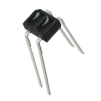


 工商网监
湘ICP备2023018690号
工商网监
湘ICP备2023018690号
