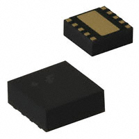
RMPA1959
PCS 3.4V CDMA & CDMA2000-1X PowerEdge™ Power Amplifier Module
General Description
Features
The RMPA1959 power amplifier module (PAM) is designed
for CDMA and CDMA2000-1X personal communications
system (PCS) applications. The 2 stage PAM is internally
matched to 50Ω to minimize the use of external
components and features advanced DC power
management to reduce current consumption during peak
phone usage. High power-added efficiency and excellent
linearity are achieved using our InGaP Heterojunction
Bipolar Transistor (HBT) technology.
• Single positive-supply operation and low power and
shutdown modes
• 39% CDMA efficiency at +28dBm average output power
• Compact LCC package- 4.0 x 4.0 x 1.5 mm with industry
standard pinout
• Internally matched to 50Ω and DC blocked RF input/
output.
• Meets CDMA2000-1XRTT performance requirements
Device
Absolute Ratings1
Symbol
Vcc1, Vcc2
Vref
Vmode
Pin
TSTG
Parameter
Supply Voltages
Reference Voltage
Power Control Voltage
RF Input Power
Storage Temperature
Min
0
2.6
0
–
-55
Max
5.0
3.5
3.5
+10
+150
Units
V
V
V
dBm
°C
Note:
1: No permanent damage with only one parameter set at extreme limit. Other parameters set to typical values.
©2004 Fairchild Semiconductor Corporation
RMPA1959 Rev. D
RMPA1959
September 2004
�RMPA1959
Module Block Diagram
VCC1, VCC2
(1, 10)
PA MODULE
COLLECTOR
BIAS
GND
(3, 6, 7, 9, 11)
INTERSTAGE
MATCH
RF IN
(2)
INPUT
MATCHING
NETWORK
INPUT
STAGE
INPUT STAGE
BIAS
VREF
(5)
OUTPUT
STAGE
MMIC
OUTPUT
MATCHING
NETWORK
RF OUT
(8)
OUTPUT STAGE
BIAS
VCC=3.4V (nom)
VREF=2.85V (nom)
1850–1910 MHz
50 Ohms I/O
BIAS
CONTROL
Vmode (4)
Figure 1. RMPA1959 US PCS CDMA Power Amplifier Module Functional Block Diagram
Electrical Characteristics1
Symbol
Parameter
Operating Frequency
f
CDMA Operation
Small-Signal Gain
SSg
Condition
Min
1850
Typ
Max
1910
Units
MHz
PO = 0dBm
23
25
dB
Gp
Power Gain
PO = +28dBm, Vmode = 0V
PO = +16dBm, Vmode ≥ 2.0V
25
28
24.5
PO
Linear Output Power
Vmode = 0V
Vmode ≥ 2.0V
Vmode = 0V
Vmode ≥ 2.0V
Vmode ≥ 2.0V, VCC = 1.4V
PO = +28dBm, Vmode = 0V
PO = +16dBm, Vmode = 2.0V
IS-95
PO = +28dBm; Vmode = 0V
PO = +16dBm; Vmode = 2.0V
PO = +28dBm; Vmode = 0V
PO = +16dBm; Vmode = 2.0V
28
dB
dB
dBm
dBm
%
%
%
mA
mA
ACPR1
PAEd (digital) @ +28 dBm
PAEd (digital) @ +16 dBm
PAEd (digital) @ +16 dBm
High Power Total Current
Low Power Total Current
Adjacent Channel Power Ratio
±1.25 MHz Offset
ACPR2
±2.25 MHz Offset
PAEd
Itot
General Characteristics
VSWR Input Impedance
Noise Figure
NF
Rx No Receive Band Noise Power
2fo-5fo Harmonic Suppression
Spurious Outputs2,3
S
Ruggedness w/Load Mismatch3
Case Operating Temperature
Tc
DC Characteristics
Quiescent Current
Iccq
Reference Current
Iref
Icc (off) Leakage Shutdown Current
16
36
39
10
20
460
120
-50
-52
-60
-68
2.5:1
PO ≤ +28dBm; 1850 to 1910 MHz
PO ≤ +28dBm
Load VSWR ≤ 5.0:1
No permanent damage
-46
-57
2.0:1
4
-139
-30
-60
10:1
85
-30
Vmode ≥ 2.0V
PO ≤ +28dBm
No applied RF signal
530
50
5
1
8
5
dBc
dBc
dBc
dBc
dB
dBm/Hz
dBc
dBc
°C
mA
mA
µA
Notes:
1: All parameters met at Tc = +25°C, Vcc = +3.4V, f = 1880 MHz, and load VSWR ≤ 1.2:1.
2: All phase angles.
3: Guaranteed by design
©2004 Fairchild Semiconductor Corporation
RMPA1959 Rev. D
�RMPA1959
I/O 1 INDICATOR
TOP VIEW
+.100
(4.00mm –.050 ) SQUARE
1
10
2
9
3
4
5
PA1959
PPYYWW
U31XX
8
7
6
1.60mm MAX.
FRONT VIEW
.25mm TYP.
SEE DETAIL A
3.50mm TYP.
.40mm
.10mm
.30mm TYP.
.10mm
.40mm
.85mm TYP.
11
.45mm
3.65mm
2
1
1.08mm
1.84mm
.18mm
BOTTOM VIEW
DETAIL A
TYP.
Figure 2. Package Outline
Package Pinout
Parameter
RF
DC Power
Ground
Control
©2004 Fairchild Semiconductor Corporation
Symbol
RF In
RF Out
Vcc1
Vcc2
Gnd
Vmode
Vref
Description
RF Input Signal
RF Output Signal
Supply Voltage to Input Stage
Supply Voltage to Output Stage
Signal Ground
Paddle Ground
High Power/Low Power Mode Control
Reference Voltage
Pin#
2
8
1
10
3, 6, 7, 9
11
4
5
RMPA1959 Rev. D
�RMPA1959
MATERIALS LIST
QTY ITEM NO.
PART NUMBER
DESCRIPTION
PC, BOARD
VENDOR
1
1
G657553-1 V2
FAIRCHILD
2
2
#142-0701-841
SMA CONNECTOR
JOHNSON
5
3
#2340-5211TN
TERMINALS
3M
FAIRCHILD
REF
4
G657584
ASSEMBLY, RMPA1959
3
5
GRM39X7R102K50V
1000 pF CAPACITOR (0603)
MURATA
3
5 (ALT) ECJ-1VB1H102K
1000 pF CAPACITOR (0603)
PANASONIC
2
6
C3216X5R1A335M
3.3 µF CAPACITOR (1206)
TDK
1
7
GRM39Y5V104Z16V
0.1µF CAPACITOR (0603)
MURATA
1
7 (ALT) ECJ-1VB1C104K
0.1µF CAPACITOR (0603)
PANASONIC
A/R
8
SN63
SOLDER PASTE
INDIUM CORP.
A/R
9
SN96
SOLDER PASTE
INDIUM CORP.
Figure 3. Evaluation Board Layout
DC Turn-On Sequence
1) Vcc1 = Vcc2 = 3.4V (typ)
2) Vref = 2.85V (typ)
3) High-Power: Vmode = 0V (Pout > 16dBm)
Low-Power: Vmode = 2.0V (Pout < 16dBm)
©2004 Fairchild Semiconductor Corporation
RMPA1959 Rev. D
�RMPA1959
Evaluation Board Schematic
3.3 µF
1
Vcc1
10
Vcc2
2
SMA1
RF IN
50 ohm
TRL
4
Vmode
5
Vref
3.3 µF
1000 pF
1000 pF
PA1959
PPYYWW
U31XX
50 ohm
TRL
8
SMA2
RF OUT
3,6,7,9
11
1000 pF
0.1 µF
(package
base)
Recommended Operating Conditions
Parameter
Operating Frequency
Supply Voltage
Reference Voltage
(operating)
(shutdown)
Bias Control Voltage (low-power)
(high-power)
Linear Output Power (high-power)
(low-power)
Case Operating Temperature
©2004 Fairchild Semiconductor Corporation
Symbol
f
Vcc1, Vcc2
Vref
Vmode
Min
1850
3.0
2.7
0
1.8
0
Pout
Tc
-30
Typ
3.4
2.85
2.0
Max
1910
4.2
3.1
0.5
3.0
0.5
+28
+16
+85
Units
MHz
V
V
V
V
V
dBm
dBm
°C
RMPA1959 Rev. D
�RMPA1959
Performance Data
RMPA1959
Vcc=3.4V, Vref = 2.85V, Pout=28dBm, Vmode=0V
33
43
32
42
31
41
30
40
PAE (%)
Gain (dB)
RMPA1959
Vcc=3.4V, Vref = 2.85V, Pout=28dBm, Vmode=0V
29
28
39
38
27
37
26
36
25
1840
1860
1880
Frequency (MHz)
1900
35
1840
1920
-55
-46
-56
-47
-57
-48
-58
ACPR2 (dBc)
APCR1 (dBc)
-45
-49
-50
-51
-52
-61
-62
-63
-64
-55
1900
1920
-60
-54
1880
Frequency (MHz)
1900
-59
-53
1860
1880
Frequency (MHz)
RMPA1959
Vcc=3.4V, Vref = 2.85V, Pout=28dBm, Vmode=0V, IS-95
RMPA1959
Vcc=3.4V, Vref = 2.85V, Pout=28dBm, Vmode=0V, IS-95
1840
1860
-65
1840
1920
1860
1880
Frequency (MHz)
1900
1920
1900
1920
1900
1920
RMPA1959 16dBm Pout
Vcc = 3.4V, Vref = 2.85V
Vmode = 2.0V
RMPA1959 16dBm Pout
Vcc = 3.4V, Vref = 2.85V
Vmode = 2.0V
12
28
27
11
PAE (%)
Gain (dB)
26
25
10
9
24
8
23
22
1840
1860
1880
Frequency (MHz)
1900
7
1840
1920
1860
RMPA1959 16dBm Pout
Vcc = 3.4V, Vref = 2.85V
Vmode = 2.0V
-40
-60
-45
-65
APCR2 (dBc)
APCR1 (dBc)
RMPA1959 16dBm Pout
Vcc = 3.4V, Vref = 2.85V
Vmode = 2.0V
-50
-55
-60
1840
1880
Frequency (MHz)
-70
-75
1860
©2004 Fairchild Semiconductor Corporation
1880
Frequency (MHz)
1900
1920
-80
1840
1860
1880
Frequency (MHz)
RMPA1959 Rev. D
�In addition to high-power/low-power bias modes, the
efficiency of the PA module can be significantly increased
at backed-off RF power levels by dynamically varying the
supply voltage (Vcc) applied to the amplifier. Since mobile
handsets and power amplifiers frequently operate at 10–20
dB back-off, or more, from maximum rated linear power,
battery life is highly dependent on the DC power consumed
at antenna power levels in the range of 0 to +16 dBm. The
reduced demand on transmitted RF power allows the PA
supply voltage to be reduced for improved efficiency, while
still meeting linearity requirements for CDMA modulation
with excellent margin. High-efficiency DC-DC converters
are now available to implement switched-voltage operation.
The following figures show measured performance of the
PA module in low-power mode (Vmode = +2.0V) at
+16dBm output power and over a range of supply voltages
from 3.4V nominal down to 1.2V. Power-added efficiency is
more than doubled from 10 percent to nearly 25 percent
(Vcc = 1.2V) while maintaining a typical ACPR1 of –52dBc
and ACPR2 of less than –61dBc.
Operation at even lower levels of Vcc supply voltage are
possible with a further restriction on the maximum RF
output power. As shown below, the PA module can be
biased at a supply voltage of as low as 0.7V with an
efficiency as high as 10–12 percent at +8dBm output
power. Excellent signal linearity is still maintained even
under this low supply voltage condition.
RMPA1959 PCS 4x4mm2 PAM
Vref = 2.85V, Pout=16dBm
RMPA1959 PCS 4x4mm2 PAM
Vref = 2.85V, Pout=16dBm
30
35
29
30
28
26
25
24
23
22
Vcc=2.0V
Vcc=1.5V
Vcc=1.5V
20
Vcc=2.0V
15
Vcc=1.2V
Vcc=3.0V
10
21
Vcc=3.4V
20
1840
1860
1880
Frequency (MHz)
1900
5
1840
1920
1880
Frequency (MHz)
1900
1920
-55
Vcc=1.2V
Vcc=1.5V
Vcc=2.0V
Vcc=3.0V
Vcc=3.4V
-44
-46
-48
-57
-59
ACPR2 (dBc)
-42
ACPR1 (dBc)
1860
RMPA1959 PCS 4x4mm2 PAM
Vref = 2.85V, Pout=16dBm
RMPA1959 PCS 4x4mm2 PAM
Vref = 2.85V, Pout=16dBm
-40
-50
-52
-54
-61
-65
-67
-71
-73
©2004 Fairchild Semiconductor Corporation
1880
Frequency (MHz)
1900
1920
Vcc=2.0V
Vcc=1.5V
-69
-58
1860
Vcc=1.2V
-63
-56
-60
1840
Vcc=1.2V
25
Vcc=3.0V
Vcc=3.4V
PAE (%)
Gain (dB)
27
-75
1840
Vcc=3.4V
1860
Vcc=3.0V
1880
Frequency (MHz)
1900
1920
RMPA1959 Rev. D
RMPA1959
Efficiency Improvement Application
�RMPA1959
Efficiency Improvement Application (continued)
RMPA1959 PCS 4x4mm2 PAM
Vref = 2.85V, Pout=16dBm, Freq=1.88GHz
RMPA1959 PCS 4x4mm2 PAM
Vref = 2.85V, Pout=16dBm, Freq=1.88GHz
30
30
28
25
PAE (%)
Gain (dB)
26
24
22
20
15
20
10
18
16
5
0.5
1
1.5
2
2.5
Vcc (V)
3
3.5
0.5
4
-40
-55
-42
-57
-44
-59
-46
-61
-48
-50
-52
-54
2.5
Vcc (V)
3
3.5
4
-65
-67
-69
-71
-58
-73
-75
0.5
1
1.5
2
2.5
Vcc (V)
3
3.5
4
0.5
1
RMPA1959 PCS 4x4mm2 PAM
Vref = 2.85V, Pout=8dBm, Freq=1.88GHz
1.5
2
2.5
Vcc (V)
3
3.5
4
RMPA1959 PCS 4x4mm2 PAM
Vref = 2.85V, Pout=8dBm, Freq=1.88GHz
30
16
28
14
12
PAE (%)
26
Gain (dB)
2
-63
-56
-60
24
22
20
10
8
6
4
18
2
16
0
0.5
1
1.5
2
2.5
Vcc (V)
3
3.5
4
0.5
1
RMPA1959 PCS 4x4mm2 PAM
Vref = 2.85V, Pout=8dBm, Freq=1.88GHz
1.5
2
2.5
Vcc (V)
3
3.5
4
RMPA1959 PCS 4x4mm2 PAM
Vref = 2.85V, Pout=8dBm, Freq=1.88GHz
-45
-60
-47
-62
-49
-64
-51
-66
ACPR2 (dBc)
ACPR1 (dBc)
1.5
RMPA1959 PCS 4x4mm2 PAM
Vref = 2.85V, Pout=16dBm, Freq=1.88GHz
ACPR2 (dBc)
ACPR1 (dBc)
RMPA1959 PCS 4x4mm2 PAM
Vref = 2.85V, Pout=16dBm, Freq=1.88GHz
1
-53
-55
-57
-68
-70
-72
-59
-74
-61
-76
-63
-78
-65
-80
0.5
1
1.5
©2004 Fairchild Semiconductor Corporation
2
2.5
Vcc (V)
3
3.5
4
0.5
1
1.5
2
2.5
Vcc (V)
3
3.5
4
RMPA1959 Rev. D
�CAUTION: THIS IS AN ESD SENSITIVE DEVICE
Precautions to Avoid Permanent Device Damage:
• Cleanliness: Observe proper handling procedures to
ensure clean devices and PCBs. Devices should remain
in their original packaging until component placement to
ensure no contamination or damage to RF, DC & ground
contact areas.
• Device Cleaning: Standard board cleaning techniques
should not present device problems provided that the
boards are properly dried to remove solvents or water
residues.
• Static Sensitivity: Follow ESD precautions to protect
against ESD damage:
– A properly grounded static-dissipative surface on
which to place devices.
– Static-dissipative floor or mat.
– A properly grounded conductive wrist strap for each
person to wear while handling devices.
• General Handling: Handle the package on the top with a
vacuum collet or along the edges with a sharp pair of
bent tweezers. Avoiding damaging the RF, DC, & ground
contacts on the package bottom. Do not apply excessive
pressure to the top of the lid.
• Device Storage: Devices are supplied in heat-sealed,
moisture-barrier bags. In this condition, devices are
protected and require no special storage conditions.
Once the sealed bag has been opened, devices should
be stored in a dry nitrogen environment.
Device Usage:
Fairchild recommends the following procedures prior to
assembly.
• Dry-bake devices at 125°C for 24 hours minimum. Note:
The shipping reels cannot withstand 125°C baking
temperature.
• Assemble the dry-baked devices within 7 days of
removal from the oven.
• During the 7-day period, the devices must be stored in an
environment of less than 60% relative humidity and a
maximum temperature of 30°C
Solder Materials & Temperature Profile: Reflow
soldering is the preferred method of SMT attachment. Hand
soldering is not recommended.
• Reflow Profile
– Ramp-up: During this stage the solvents are
evaporated from the solder paste. Care should be
taken to prevent rapid oxidation (or paste slump) and
solder bursts caused by violent solvent out-gassing. A
typical heating rate is 1- 2°C/sec.
– Pre-heat/soak: The soak temperature stage serves
two purposes; the flux is activated and the board and
devices achieve a uniform temperature. The
recommended soak condition is: 120-150 seconds at
150°C.
– Reflow Zone: If the temperature is too high, then
devices may be damaged by mechanical stress due to
thermal mismatch or there may be problems due to
excessive solder oxidation. Excessive time at
temperature can enhance the formation of intermetallic compounds at the lead/board interface and
may lead to early mechanical failure of the joint.
Reflow must occur prior to the flux being completely
driven off. The duration of peak reflow temperature
should not exceed 10 seconds. Maximum soldering
temperatures should be in the range 215-220°C, with
a maximum limit of 225°C.
– Cooling Zone: Steep thermal gradients may give rise
to excessive thermal shock. However, rapid cooling
promotes a finer grain structure and a more crackresistant solder joint. The illustration below indicates
the recommended soldering profile.
Solder Joint Characteristics:
Proper operation of this device depends on a reliable voidfree attachment of the heatsink to the PWB. The solder joint
should be 95% void-free and be a consistent thickness.
Rework Considerations:
Rework of a device attached to a board is limited to reflow
of the solder with a heat gun. The device should not be
subjected to more than 225°C and reflow solder in the
molten state for more than 5 seconds. No more than 2
rework operations should be performed.
• If the 7-day period or the environmental conditions have
been exceeded, then the dry-bake procedure must be
repeated.
©2004 Fairchild Semiconductor Corporation
RMPA1959 Rev. D
RMPA1959
Application Information
�RMPA1959
240
10 SEC
220
200
183°C
180
160
140
DEG (°C)
120
100
1°C/SEC
SOAK AT 150°C
FOR 60 SEC
80
45 SEC (MAX)
ABOVE 183°C
1°C/SEC
60
40
20
0
0
60
120
180
240
300
TIME (SEC)
Figure 4. Recommended Solder Reflow Profile
©2004 Fairchild Semiconductor Corporation
RMPA1959 Rev. D
�TRADEMARKS
The following are registered and unregistered trademarks Fairchild Semiconductor owns or is authorized to use and is
not intended to be an exhaustive list of all such trademarks.
ACEx™
FAST
ActiveArray™
FASTr™
Bottomless™ FPS™
CoolFET™
FRFET™
CROSSVOLT™ GlobalOptoisolator™
DOME™
GTO™
EcoSPARK™ HiSeC™
E2CMOS™
I2C™
EnSigna™
i-Lo™
FACT™
ImpliedDisconnect™
FACT Quiet Series™
ISOPLANAR™
LittleFET™
MICROCOUPLER™
MicroFET™
MicroPak™
MICROWIRE™
MSX™
MSXPro™
OCX™
OCXPro™
OPTOLOGIC
Across the board. Around the world.™ OPTOPLANAR™
PACMAN™
The Power Franchise
POP™
Programmable Active Droop™
Power247™
PowerEdge™
PowerSaver™
PowerTrench
QFET
QS™
QT Optoelectronics™
Quiet Series™
RapidConfigure™
RapidConnect™
µSerDes™
SILENT SWITCHER
SMART START™
SPM™
Stealth™
SuperFET™
SuperSOT™-3
SuperSOT™-6
SuperSOT™-8
SyncFET™
TinyLogic
TINYOPTO™
TruTranslation™
UHC™
UltraFET
VCX™
DISCLAIMER
FAIRCHILD SEMICONDUCTOR RESERVES THE RIGHT TO MAKE CHANGES WITHOUT FURTHER NOTICE TO ANY
PRODUCTS HEREIN TO IMPROVE RELIABILITY, FUNCTION OR DESIGN. FAIRCHILD DOES NOT ASSUME ANY LIABILITY
ARISING OUT OF THE APPLICATION OR USE OF ANY PRODUCT OR CIRCUIT DESCRIBED HEREIN; NEITHER DOES IT
CONVEY ANY LICENSE UNDER ITS PATENT RIGHTS, NOR THE RIGHTS OF OTHERS.
LIFE SUPPORT POLICY
FAIRCHILD’S PRODUCTS ARE NOT AUTHORIZED FOR USE AS CRITICAL COMPONENTS IN LIFE SUPPORT
DEVICES OR SYSTEMS WITHOUT THE EXPRESS WRITTEN APPROVAL OF FAIRCHILD SEMICONDUCTOR CORPORATION.
As used herein:
2. A critical component is any component of a life
1. Life support devices or systems are devices or
support device or system whose failure to perform can
systems which, (a) are intended for surgical implant into
be reasonably expected to cause the failure of the life
the body, or (b) support or sustain life, or (c) whose
support device or system, or to affect its safety or
failure to perform when properly used in accordance
with instructions for use provided in the labeling, can be
effectiveness.
reasonably expected to result in significant injury to the
user.
PRODUCT STATUS DEFINITIONS
Definition of Terms
Datasheet Identification
Product Status
Definition
Advance Information
Formative or
In Design
This datasheet contains the design specifications for
product development. Specifications may change in
any manner without notice.
Preliminary
First Production
This datasheet contains preliminary data, and
supplementary data will be published at a later date.
Fairchild Semiconductor reserves the right to make
changes at any time without notice in order to improve
design.
No Identification Needed
Full Production
This datasheet contains final specifications. Fairchild
Semiconductor reserves the right to make changes at
any time without notice in order to improve design.
Obsolete
Not In Production
This datasheet contains specifications on a product
that has been discontinued by Fairchild semiconductor.
The datasheet is printed for reference information only.
Rev. I13
�