STK672-040GEVB,
STK672-050GEVB,
STK672-060GEVB
STK672 Series Evaluation
Board User's Manual
Thick−Film Hybrid IC Unipolar
Constant−current Chopper (external
Excitation PWM) Circuit with Built−in
Microstepping Controller Stepping Motor
Driver (sine wave drive)
http://onsemi.com
EVAL BOARD USER’S MANUAL
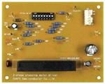
Figure 1. STK672 Series Evaluation Boards
This Evaluation Board User’s Manual describes the set-up and use of the STK672 Series Evaluation Board for
SANYO Semiconductor (An ON Semiconductor Company) Thick-Film Hybrid IC Unipolar Constant-Current Chopper
Circuit with Built-in Microstepping Controller Stepping Motor Driver devices STK672-040-E, STK672-050-E, and
STK672-060-E. For datasheets and additional information on these devices, please visit the ON Semiconductor website at
www.onsemi.com
© Semiconductor Components Industries, LLC, 2012
March, 2012 − Rev. 0
1
Publication Order Number:
EVBUM2089/D
�STK672−040GEVB, STK672−050GEVB, STK672−060GEVB
EVALUATION BOARD
STK672−040−E and STK672−060−E (100.0 mm x 80.0 mm x 1.6 mm, phenol 1−layer board)
Function
Generator
Peak to peak 5.0 V − 0 V
Clock pulse
2−phase
stepping motor
Vcc1
power
supply
Vcc2
power
supply
Figure 2. STK672−040−E / STK672−060−E Evaluation Board
http://onsemi.com
2
�STK672−040GEVB, STK672−050GEVB, STK672−060GEVB
EVALUATION BOARD
STK672−050−E (100.0 mm x 80.0 mm x 1.6 mm, phenol 1−layer board)
Function
Generator
Peak to peak 5.0 V − 0 V
Clock pulse
2−phase
stepping motor
Vcc1
power
supply
Vcc2
power
supply
Figure 3. STK672−050−E Evaluation Board
http://onsemi.com
3
�STK672−040GEVB, STK672−050GEVB, STK672−060GEVB
SUBSTRATE SPECIFICATIONS
(Substrate recommended for operation of STK672−050−E)
Size: 100 mm x 80 mm x 1.6 mm 1−layer board
Material: Phenol
Figure 4. Copper Side (35 m)
ALLOWABLE POWER DISSIPATION (Reference value)
5.5
5.2 W
STK672−050−E
Allowable power dissipation Pdmax W
5
4.7 W
4.5
STK672−040−E
STK672−060−E
4
3.5
3
2.5
2
1.5
1
0.5
0
0
20
40
60
80
Ambient temperature, Ta− °C
Figure 5. Allowable Power Dissipation
http://onsemi.com
4
100
120
�STK672−040GEVB, STK672−050GEVB, STK672−060GEVB
EVALUATION CIRCUIT
2-phase stepping motor
CLK
RETURN
R11 R10
Vref
ENABLE
R02
MOI
JP2
R01
MO1
MO2
R08
R03 R09
CN1
R05
R07
R06
A
JP1
R04
Vcc2(5V)
AB
B
BB COMA
COMB
D1
1
2
R12
C3
C4
Slide swich
GND
(Pin22)
Vcc1
4
5
6
7
8
C1
C2
GND(PG)
9
8
7
6
5
4
3
2
1
Hybrid IC: STK672-050(040, 060)
Figure 6. Evaluation Circuit
http://onsemi.com
5
BB
B
PG
PG
AB
A
Vcc2
Vref
M1
M2
M3
M4
M5
CLK
GND(SG)
CWB
RESETB
RETURN
ENABLE
MOI
MO1
MO2
SG
22 21 20 19 18 17 16 15 14 13 12 11 10
�STK672−040GEVB, STK672−050GEVB, STK672−060GEVB
BILL OF MATERIALS
Table 1. BILL OF MATERIALS FOR STK672−050−E EVALUATION BOARD
Substitution
Lead
Allowed
Free
50ME220CA
YES
YES
SUN ELECTRONICS
50ME10CA
YES
YES
±20%
SUN ELECTRONICS
50ME10CA
YES
YES
±10%
Panasonic
ECQV1H104JL2
YES
YES
Resistor to
set Vref
±1%
AKAHANE
ELECTRONICS
RN14S****FK
YES
YES
1
Resistor to
set Vref
±1%
AKAHANE
ELECTRONICS
RN14S****FK
YES
YES
R03 to
R11
9
Pull-up
Resistor
10 kW
±5%
AKAHANE
ELECTRONICS
RN14S103JK
YES
YES
R12
1
Resistor for
power on
reset circuit
1 kW
±5%
AKAHANE
ELECTRONICS
RN14S102JK
YES
YES
D1
1
Diode for
power on
reset circuit
SANYO Semiconductor
DS135AE
YES
YES
Hybrid IC
SANYO Semiconductor
STK672-050
NO
YES
5045-06A
YES
YES
JS01-08AP4-ST
YES
YES
Designator
QTY
Description
Value
C1
1
Vcc1 Bypass
Capacitor
220 mF
/ 50 V
±20%
SUN ELECTRONICS
C2
1
Vcc2 Bypass
Capacitor
10 mF
/ 50 V
±20%
C3
1
Capacitor for
power on
reset circuit
10 mF
/ 50 V
C4
1
Vref
stabilization
Capacitor
0.1 mF
/ 50 V
R01
1
R02
HIC
1
Tolerance
Footprint
Manufacturer
Manufacturer
Part Number
(An ON Semiconductor
Company)
(An ON Semiconductor
Company)
CN1
1
Vertical
Header
MOLEX
Slide
switch
1
Dip slide
switch
NIHON KAIHEIKI
JP1,
JP2
2
Jumper
Mac-Eight
JR-4
YES
YES
TP1 to
TP12
12
Test Point
Mac-Eight
ST-1-3
YES
YES
NOTE: R01 and R02 are used to Vref for current setting.
Therefore their value is not mentioned in this table.
http://onsemi.com
6
�STK672−040GEVB, STK672−050GEVB, STK672−060GEVB
S�TK672-�060-�E Tc -� Ope�rating ti�me
70
Ope�rating� Temperature
Tc ℃
60
50
40
1.2A
30
1.0A
20
0.8A
10
0
2
4
6
8
10
12
14
16
Ope�rating t�im�e m�in
(Condition: Ta=2�5℃ 1/4step 2000pps Mot�or L�=2�.2�m�H/�R=1�.5 Ω
b�y Evaluation� Bo�ar�d)
18
V�cc=2�4�V
20
V�DD=5�.0�V
S�TK672-�040-�E Tc -� Ope�rating ti�me
70
Ope�rating Temperature
Tc ℃
60
50
40
1.5A
30
1.25A
20
1.0A
10
0
2
4
6
8
10
12
14
16
18
Ope�rating t�im�e m�in
(Condition: Ta=2�5℃ 1/4step 2000pps Mot�or L�=2�.2�m�H/�R=1�.5 Ω
b�y Evaluation� Bo�ar�d)
V�cc=2�4�V
20
V�DD=5�.0�V
S�TK672-�050-�E Tc -� Ope�rating ti�me
Ope�rating Temperature
Tc ℃
110
100
90
80
70
60
50
40
30
20
10
2.5A
2.0A
1.5A
3.0A with heat sink
0
2
4
6
8
10
12
14
16
18
20
Ope�r�at�ing t�im�e m�in
(Condition: Ta=2�5 ℃ 1/4step 2000pps Mot�or L�=2�.2�m�H/�R=1�.5 Ω V�cc=2�4�V
b�y Evaluation� Board)
Figure 7. Operating Temperature
http://onsemi.com
7
2.5A with heat sink
V�DD=5�.0�V
�STK672−040GEVB, STK672−050GEVB, STK672−060GEVB
NOTES: Heat sink size used in STK672-050-E
IOH = 3.0 A and 2.5 A: 100 mm X 70 mm X
2.0 mm Al plate (no surface finish)
The Tc temperature should be checked in the
center of the metal surface of the product
package.
EVALUATION BOARD SETUP
[Setting the motor current]
The motor current IOH is set by the Vref voltage on the
hybrid IC pin 8. The following formula gives the
relationship between IOH and Vref.
[Supply Voltage]
Vcc1 (10 to 45 V): Power Supply for stepping motor
Vref (0 to 2.5 V): Const. Current Control for Reference
Voltage
Vcc2 (5 V): Power Supply for internal logic IC
STK672-040-E
IOH=(1/3) x Vref/Rs, Rs: The hybrid IC internal current
detection resistor (0.33 W 3%)
Vref = Vcc2 (5.0 V) x R02 / (R01 + R02) = IOH x Rs x 3
In case of IOH = 1.2 A, Vref = 1.2 x 0.33 x 3 = 1.19 V
[Toggle Switch State]
ON Side: Low (GND)
OFF Side: High (5 V pull up resistors)
[Operation Guide]
1. Motor Connection:
Connect the stepping motor to A, AB, B, BB,
COMA, and COMB.
2. Initial Condition Setting:
Set “ON” the slide switch RESETB, and set “ON
or OFF” M1 to M5 depend on step mode, and set
“ON or OFF” CWB, and set low CLK.
3. Power Supply:
At first, supply DC voltage to Vcc2, and VREF.
Next, supply DC voltage to Vcc1.
4. Ready for Operation from Standby State:
Turn “OFF” the slide switch RESETB.
Output A and BB are set initial position 70%.
5. Motor Operation:
Input the CLK signal into the terminal CLK.
STK672−050−E
IOH=(1/3) x Vref/Rs, Rs: The hybrid IC internal current
detection resistor (0.2 W 3%)
Vref = Vcc2 (5.0 V) x R02 / (R01 + R02) = IOH x Rs x 3
In case of IOH = 2.0 A, Vref = 2.0 x 0.2 x 3 = 1.2 V
STK672−060−E
IOH=(1/7.66) x Vref/Rs, Rs: The hybrid IC internal current
detection resistor (0.22 W 3%)
Vref = Vcc2 (5.0 V) x R02 / (R01 + R02) = IOH x Rs x 7.66
In case of IOH = 0.8 A, Vref = 0.8 x 0.22 x 7.66 = 1.35 V
http://onsemi.com
8
�onsemi,
, and other names, marks, and brands are registered and/or common law trademarks of Semiconductor Components Industries, LLC dba “onsemi” or its affiliates
and/or subsidiaries in the United States and/or other countries. onsemi owns the rights to a number of patents, trademarks, copyrights, trade secrets, and other intellectual property. A
listing of onsemi’s product/patent coverage may be accessed at www.onsemi.com/site/pdf/Patent−Marking.pdf. onsemi is an Equal Opportunity/Affirmative Action Employer. This
literature is subject to all applicable copyright laws and is not for resale in any manner.
The evaluation board/kit (research and development board/kit) (hereinafter the “board”) is not a finished product and is not available for sale to consumers. The board is only intended
for research, development, demonstration and evaluation purposes and will only be used in laboratory/development areas by persons with an engineering/technical training and familiar
with the risks associated with handling electrical/mechanical components, systems and subsystems. This person assumes full responsibility/liability for proper and safe handling. Any
other use, resale or redistribution for any other purpose is strictly prohibited.
THE BOARD IS PROVIDED BY ONSEMI TO YOU “AS IS” AND WITHOUT ANY REPRESENTATIONS OR WARRANTIES WHATSOEVER. WITHOUT LIMITING THE FOREGOING,
ONSEMI (AND ITS LICENSORS/SUPPLIERS) HEREBY DISCLAIMS ANY AND ALL REPRESENTATIONS AND WARRANTIES IN RELATION TO THE BOARD, ANY
MODIFICATIONS, OR THIS AGREEMENT, WHETHER EXPRESS, IMPLIED, STATUTORY OR OTHERWISE, INCLUDING WITHOUT LIMITATION ANY AND ALL
REPRESENTATIONS AND WARRANTIES OF MERCHANTABILITY, FITNESS FOR A PARTICULAR PURPOSE, TITLE, NON−INFRINGEMENT, AND THOSE ARISING FROM A
COURSE OF DEALING, TRADE USAGE, TRADE CUSTOM OR TRADE PRACTICE.
onsemi reserves the right to make changes without further notice to any board.
You are responsible for determining whether the board will be suitable for your intended use or application or will achieve your intended results. Prior to using or distributing any systems
that have been evaluated, designed or tested using the board, you agree to test and validate your design to confirm the functionality for your application. Any technical, applications or
design information or advice, quality characterization, reliability data or other services provided by onsemi shall not constitute any representation or warranty by onsemi, and no additional
obligations or liabilities shall arise from onsemi having provided such information or services.
onsemi products including the boards are not designed, intended, or authorized for use in life support systems, or any FDA Class 3 medical devices or medical devices with a similar
or equivalent classification in a foreign jurisdiction, or any devices intended for implantation in the human body. You agree to indemnify, defend and hold harmless onsemi, its directors,
officers, employees, representatives, agents, subsidiaries, affiliates, distributors, and assigns, against any and all liabilities, losses, costs, damages, judgments, and expenses, arising
out of any claim, demand, investigation, lawsuit, regulatory action or cause of action arising out of or associated with any unauthorized use, even if such claim alleges that onsemi was
negligent regarding the design or manufacture of any products and/or the board.
This evaluation board/kit does not fall within the scope of the European Union directives regarding electromagnetic compatibility, restricted substances (RoHS), recycling (WEEE), FCC,
CE or UL, and may not meet the technical requirements of these or other related directives.
FCC WARNING – This evaluation board/kit is intended for use for engineering development, demonstration, or evaluation purposes only and is not considered by onsemi to be a finished
end product fit for general consumer use. It may generate, use, or radiate radio frequency energy and has not been tested for compliance with the limits of computing devices pursuant
to part 15 of FCC rules, which are designed to provide reasonable protection against radio frequency interference. Operation of this equipment may cause interference with radio
communications, in which case the user shall be responsible, at its expense, to take whatever measures may be required to correct this interference.
onsemi does not convey any license under its patent rights nor the rights of others.
LIMITATIONS OF LIABILITY: onsemi shall not be liable for any special, consequential, incidental, indirect or punitive damages, including, but not limited to the costs of requalification,
delay, loss of profits or goodwill, arising out of or in connection with the board, even if onsemi is advised of the possibility of such damages. In no event shall onsemi’s aggregate liability
from any obligation arising out of or in connection with the board, under any theory of liability, exceed the purchase price paid for the board, if any.
The board is provided to you subject to the license and other terms per onsemi’s standard terms and conditions of sale. For more information and documentation, please visit
www.onsemi.com.
PUBLICATION ORDERING INFORMATION
LITERATURE FULFILLMENT:
Email Requests to: orderlit@onsemi.com
onsemi Website: www.onsemi.com
◊
TECHNICAL SUPPORT
North American Technical Support:
Voice Mail: 1 800−282−9855 Toll Free USA/Canada
Phone: 011 421 33 790 2910
www.onsemi.com
1
Europe, Middle East and Africa Technical Support:
Phone: 00421 33 790 2910
For additional information, please contact your local Sales Representative
�


 工商网监
湘ICP备2023018690号
工商网监
湘ICP备2023018690号
