DATASHEET
IDT5V41064
1 OUTPUT PCIE GEN1/2 SYNTHESIZER
Recommended Applications
Features/Benefits
One output synthesizer for PCIe Gen1/2
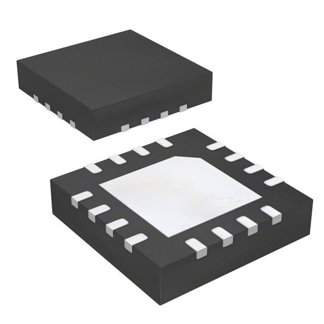
• 16-pin QFN package; very small board footprint
• Spread-spectrum capable; reduces EMI
• Outputs can be terminated to LVDS; can drive a wider
General Description
variety of devices
The IDT5V41064 is a PCIe Gen2 compliant spread
spectrum capable clock generator. The device has 1
differential HCSL output and can be used in communication
or embedded systems to substantially reduce
electro-magnetic interference (EMI). Spread spectrum can
be enabled via a select pin.
• Spread enable via pin selection; no software required to
configure device
• Industrial temperature range available; supports
demanding embedded applications
• For PCIe Gen3 applications, see the 5V41234
Output Features
Key Specifications
• 1 - 0.7V current mode differential HCSL output pairs
• Cycle-to-cycle jitter < 100 ps
• PCIe Gen2 phase jitter < 3.0ps RMS
Block Diagram
VDD
SS1
Control
Logic
CLK
Phase Lock
Loop
X1
25 MHz
crystal /clock
X2
Clock
Buffer/
Crystal
Oscillator
Crystal Tuning Capacitors
GND
IDT® 1 OUTPUT PCIE GEN1/2 SYNTHESIZER
CLK
1
RR (IREF)
IDT5V41064
APRIL 17, 2017
�IDT5V41064
1 OUTPUT PCIE GEN1/2 SYNTHESIZER
GND
NC
VDD
Spread Spectrum Select Table
NC
NC
Pin Assignment
13
1
CLK
X1
CLK
X2
GND
NC
0
-0.5% down
1
No spread
NC
IREF
SS1
GND
Spread%
VDDA
9
5
SS1
16-pin QFN
Pin Descriptions
Pin
Number
Pin
Name
Pin Type
Pin Description
1
GND
Power
2
X1
XI
Crystal or clock input. Connect to 25 MHz crystal or single-ended clock.
3
X2
XO
Crystal connection. Connect to parallel mode crystal. Leave floating if X1 is driven by
single-ended clock.
4
NC
–
5
GND
Power
6
SS1
Input
7
IREF
Output
8
NC
–
9
VDDA
Power
Connect to 3.3V and filter as analog supply.
10
GND
Power
Connect to ground.
11
CLK
Output
HCSL complementary output clock.
12
CLK
Output
HCSL true output clock.
13
NC
–
No connect.
14
NC
–
No connect.
15
VDD
Power
16
NC
–
Connect to ground.
No connect.
Connect to ground.
Spread Select 1. See table above. Internal pull-up resistor.
475 precision resistor must be attached to this pin, which is connected to internal
current source.
No connect.
Connect to 3.3 V for OSC and digital circuits.
No connect.
IDT® 1 OUTPUT PCIE GEN1/2 SYNTHESIZER
2
IDT5V41064
APRIL 17, 2017
�IDT5V41064
1 OUTPUT PCIE GEN1/2 SYNTHESIZER
Applications Information
Output Structures
External Components
A minimum number of external components are required for
proper operation.
IREF
=2.3 mA
6*IREF
Decoupling Capacitors
Decoupling capacitors of 0.01F should be connected
between VDD and the ground plane (pin 4) as close to the
VDD pin as possible. Do not share ground vias between
components. Route power from power source through the
capacitor pad and then into IDT pin.
Crystal
A 25 MHz fundamental mode parallel resonant crystal with
CL = 16 pF should be used. This crystal must have less than
300 ppm of error across temperature in order for the
IDT5V41064 to meet PCI Express specifications.
R R 475
See Layout
Guidelines
Crystal Capacitors
General PCB Layout Recommendations
Crystal capacitors are connected from pins X1 to ground
and X2 to ground to optimize the accuracy of the output
frequency.
For optimum device performance and lowest output phase
noise, the following guidelines should be observed.
1. Each 0.01µF decoupling capacitor should be mounted on
the component side of the board as close to the VDD pin as
possible.
CL= Crystal’s load capacitance in pF
Crystal Capacitors (pF) = (CL- 8) * 2
2. No vias should be used between decoupling capacitor
and VDD pin.
For example, for a crystal with a 16 pF load cap, each
external crystal cap would be 16 pF. (16-8)*2=16.
3. The PCB trace to VDD pin should be kept as short as
possible, as should the PCB trace to the ground via.
Distance of the ferrite bead and bulk decoupling from the
device is less critical.
Current Source (Iref) Reference Resistor - RR
If board target trace impedance (Z) is 50, then RR = 475
(1%), providing IREF of 2.32 mA. The output current (IOH) is
equal to 6*IREF.
4. An optimum layout is one with all components on the
same side of the board, minimizing vias through other signal
layers (any ferrite beads and bulk decoupling capacitors can
be mounted on the back). Other signal traces should be
routed away from the IDT5V41064.This includes signal
traces just underneath the device, or on layers adjacent to
the ground plane layer used by the device.
Output Termination
The PCI-Express differential clock outputs of the
IDT5V41064 are open source drivers and require an
external series resistor and a resistor to ground. These
resistor values and their allowable locations are shown in
detail in the PCI-Express Layout Guidelines section.
The IDT5V41064 can also be terminated to LVDS
compatible voltage levels. See Layout Guidelines section.
IDT® 1 OUTPUT PCIE GEN1/2 SYNTHESIZER
3
IDT5V41064
APRIL 17, 2017
�IDT5V41064
1 OUTPUT PCIE GEN1/2 SYNTHESIZER
Layout Guidelines for PCI Express
PCIe Reference Clock
Common Recommendations for Differential Routing
Dimension or Value
L1 length, route as non-coupled 50ohm trace
0.5 max
L2 length, route as non-coupled 50ohm trace
0.2 max
L3 length, route as non-coupled 50ohm trace
0.2 max
Rs
33
Rt
49.9
Unit
inch
inch
inch
ohm
ohm
Figure
1
1
1
1
1
Down Device Differential Routing
L4 length, route as coupled microstrip 100ohm differential trace
L4 length, route as coupled stripline 100ohm differential trace
2 min to 16 max
1.8 min to 14.4 max
inch
inch
1
1
Differential Routing to PCI Express Connector
L4 length, route as coupled microstrip 100ohm differential trace
L4 length, route as coupled stripline 100ohm differential trace
0.25 to 14 max
0.225 min to 12.6 max
inch
inch
2
2
Figure 1: Down Device Routing
L2
L1
Rs
L4
L4'
L2'
L1'
Rs
Rt
HCSL Output Buffer
Rt
L3'
PCI Express
Down Device
REF_CLK Input
L3
Figure 2: PCI Express Connector Routing
L2
L1
Rs
L4
L4'
L2'
L1'
Rs
Rt
HCSL Output Buffer
Rt
L3'
IDT® 1 OUTPUT PCIE GEN1/2 SYNTHESIZER
4
PCI Express
Add-in Board
REF_CLK Input
L3
IDT5V41064
APRIL 17, 2017
�IDT5V41064
1 OUTPUT PCIE GEN1/2 SYNTHESIZER
Layout Guidelines for LVDS and Other Applications
Alternative Termination for LVDS and other Common Differential Signals (figure 3)
Vdiff
Vp-p
Vcm
R1
R2
R3
R4
Note
0.45v
0.22v
1.08
33
150
100
100
0.58
0.28
0.6
33
78.7
137
100
0.80
0.40
0.6
33
78.7
none
100
ICS874003i-02 input compatible
0.60
0.3
1.2
33
174
140
100
Standard LVDS
R1a = R1b = R1
R2a = R2b = R2
Figure 3
L2
L1
R3
R1a
R4
L4
L4'
L2'
L1'
R1b
R2a
HCSL Output Buffer
R2b
L3'
Down Device
REF_CLK Input
L3
Cable Connected AC Coupled Application (figure 4)
Component
Value
Note
R5a, R5b
8.2K 5%
R6a, R6b
1K 5%
Cc
0.1 µF
Vcm
0.350 volts
Figure 4
3.3 Volts
R5a
R5b
R6a
R6b
Cc
L4
L4'
Cc
IDT® 1 OUTPUT PCIE GEN1/2 SYNTHESIZER
5
PCIe Device
REF_CLK Input
IDT5V41064
APRIL 17, 2017
�IDT5V41064
1 OUTPUT PCIE GEN1/2 SYNTHESIZER
Typical PCI-Express (HCSL) Waveform
700 mV
0
tOR
500 ps
500 ps
0.525 V
0.175 V
tOF
0.525 V
0.175 V
Typical LVDS Waveform
1325 mV
1000 mV
tOR
500 ps
500 ps
1250 mV
1150 mV
IDT® 1 OUTPUT PCIE GEN1/2 SYNTHESIZER
tOF
1250 mV
1150 mV
6
IDT5V41064
APRIL 17, 2017
�IDT5V41064
1 OUTPUT PCIE GEN1/2 SYNTHESIZER
Absolute Maximum Ratings
Stresses above the ratings listed below can cause permanent damage to the IDT5V41064. These ratings are stress
ratings only. Functional operation of the device at these or any other conditions above those indicated in the
operational sections of the specifications is not implied. Exposure to absolute maximum rating conditions for
extended periods can affect product reliability. Electrical parameters are guaranteed only over the recommended
operating temperature range.
Item
Rating
Supply Voltage, VDD, VDDA
5.5 V
All Inputs and Outputs
-0.5 V to VDD+0.5 V
Ambient Operating Temperature (commercial)
0 to +70C
Ambient Operating Temperature (industrial)
-40 to +85C
Storage Temperature
-65 to +150C
Junction Temperature
125C
Soldering Temperature
260C
ESD Protection (Input)
2000 V min. (HBM)
DC Electrical Characteristics
Unless stated otherwise, VDD = 3.3 V ±5%, Ambient Temperature -40 to +85C
Parameter
Symbol
Supply Voltage
Input High Voltage1
Input Low Voltage
1
Conditions
Min.
Typ.
Max.
Units
V
3.135
3.465
VIH
2.2
VDD +0.3
V
VIL
VSS-0.3
0.8
V
Input Leakage Current
IIL
0 < Vin < VDD
5
A
Operating Supply Current
IDD
2 pF load
70
mA
Input Capacitance
CIN
Input pin capacitance
7
pF
Output pin capacitance
6
pF
5
nH
2
Output Capacitance
COUT
Pin Inductance
LPIN
Output Resistance
Rout
CLK outputs
Pull-up Resistor
RPUP
SS1
-5
3.0
k
100
k
1 Single edge is monotonic when transitioning through region.
2 Inputs with pull-ups/-downs are not included.
IDT® 1 OUTPUT PCIE GEN1/2 SYNTHESIZER
7
IDT5V41064
APRIL 17, 2017
�IDT5V41064
1 OUTPUT PCIE GEN1/2 SYNTHESIZER
AC Electrical Characteristics - CLK/CLK
Unless stated otherwise, VDD=3.3 V ±5%, Ambient Temperature -40 to +85C
Parameter
Symbol
Conditions
Min.
Typ.
Input Frequency
Max.
Units
25
Output Frequency
MHz
100
MHz
Output High Voltage1,2
VOH
660
700
850
mV
Voltage1,2
VOL
-150
27
150
mV
250
350
550
mV
40
140
mV
25
100
ps
Output Low
Crossing Point
Voltage1,2
Absolute
Crossing Point
Voltage1,2,4
Variation over all edges
Jitter, Cycle-to-Cycle1,3
Rise
Fall
Time1,2
Time1,2
Rise/Fall Time
tOR
From 0.175 V to 0.525 V
175
332
700
ps
tOF
From 0.525 V to 0.175 V
175
344
700
ps
75
125
ps
45
51
55
%
3.0
ms
Variation1,2
Duty Cycle1,3
Stabilization Time
tSTABLE
From power-up VDD=3.3 V
1.2
Spread Change Time
tSPREAD
Settling period after spread change
3.0
1 Test
ms
setup is RS=33 ohms RP=50 ohms with 2 pF, RR = 475 (1%).
2 Measurement
taken from a single-ended waveform.
3 Measurement
taken from a differential waveform.
4 Measured
at the crossing point where instantaneous voltages of both CLK and CLK are equal.
Electrical Characteristics - Differential Phase Jitter
Parameter
Jitter, Phase
Symbol
Conditions
Min
Typ
Max
Units
Notes
tjphasePLL
PCIe Gen1
30
86
ps (p-p)
1,2,3
tjphaseLO
PCIe Gen2, 10 kHz < f < 1.5 MHz
1.2
3
ps (RMS)
1,2,3
PCIe Gen2, 1.5 MHz < f < Nyquist (50 MHz)
1.9
3.1
ps (RMS)
1,2,3
tjphaseHIGH
Note 1. Guaranteed by design and characterization, not 100% tested in production.
Note 2. See http://www.pcisig.com for complete specs.
Note 3: Applies to 100MHz, spread off and 0.5% down spread only.
Thermal Characteristics
Parameter
Thermal Resistance Junction to
Ambient
Thermal Resistance Junction to Case
IDT® 1 OUTPUT PCIE GEN1/2 SYNTHESIZER
Symbol
Conditions
Min.
Typ.
Max. Units
JA
Still air
63.2
C/W
JA
1 m/s air flow
55.9
C/W
JA
2 m/s air flow
53.1
C/W
JA
3 m/s air flow
51.4
C/W
65.8
C/W
JC
8
IDT5V41064
APRIL 17, 2017
�IDT5V41064
1 OUTPUT PCIE GEN1/2 SYNTHESIZER
Marking Diagrams
XXX
YWW$
064G
XXX
YWW$
064GI
Notes:
1. Line 1: ‘XXX’ is the lot traceability (last numeric character of the assembly lot number).
2. Line 2: ‘YYW’ – Date code; $ – Assembly location.
3. Line 3: truncated IDT part number.
4. “G” designates RoHS compliant package.
5. “I” within the part number indicates industrial temperature range.
IDT® 1 OUTPUT PCIE GEN1/2 SYNTHESIZER
9
IDT5V41064
APRIL 17, 2017
�IDT5V41064
1 OUTPUT PCIE GEN1/2 SYNTHESIZER
10
Package Outline and Package Dimensions (16-pin QFN)
IDT® 1 OUTPUT PCIE GEN1/2 SYNTHESIZER
IDT5V41064
APRIL 17, 2017
�IDT5V41064
1 OUTPUT PCIE GEN1/2 SYNTHESIZER
11
Package Outline and Package Dimensions (16-pin QFN), cont.
IDT® 1 OUTPUT PCIE GEN1/2 SYNTHESIZER
IDT5V41064
APRIL 17, 2017
�IDT5V41064
1 OUTPUT PCIE GEN1/2 SYNTHESIZER
Ordering Information
Part / Order Number
Marking
5V41064NLG
See Page 9
Shipping Packaging
Package
Temperature
Trays
16-pin QFN
0 to +70 C
5V41064NLG8
Tape and Reel
16-pin QFN
0 to +70 C
5V41064NLGI
Trays
16-pin QFN
-40 to +85 C
5V41064NLGI8
Tape and Reel
16-pin QFN
-40 to +85 C
“G” after the two-letter package code are the Pb-Free configuration and are RoHS compliant.
While the information presented herein has been checked for both accuracy and reliability, Integrated Device Technology (IDT) assumes
no responsibility for either its use or for the infringement of any patents or other rights of third parties, which would result from its use. No
other circuits, patents, or licenses are implied. This product is intended for use in normal commercial applications. Any other applications
such as those requiring extended temperature range, high reliability, or other extraordinary environmental requirements are not
recommended without additional processing by IDT. IDT reserves the right to change any circuitry or specifications without notice. IDT
does not authorize or warrant any IDT product for use in life support devices or critical medical instruments.
Revision History
Rev.
Originator
A
Date
Description of Change
04/01/08
Initial release - preliminary.
B
RW
03/02/10
1. Updated Title and Features bullets
2. Added Differential Phase Jitter table
3. Updated Cycle-to-cycle Jitter spec from 80ps to 125ps
C
RDW
06/18/10
1. Updated package and pinout to 16QFN.
2. Added Spread Spectrum.
D
RDW
07/19/10
1. Updated title and general description
2. Updated cycle-to-cycle jitter spec from 125 to 100 ps
E
RDW
12/21/10
1. Minor corrections
2. Updated with Typical data
3. Released to final
F
RDW
10/28/11
Updated Thermal char data
G
RDW
11/21/11
1. Changed title to “1 Output PCIe GEN1/2 Synthesizer”
2. Added note to Features section: “For PCIe Gen3 applications, see 5V41234”
3. Updated Differential Phase Jitter table.
H
RDW
10/07/13
Updated VOH min and VOL max values in AC Char table.
J
C.P.
04/17/17
Replaced package outline drawings with latest NLG16 drawings.
IDT® 1 OUTPUT PCIE GEN1/2 SYNTHESIZER
12
IDT5V41064
APRIL 17, 2017
�IDT5V41064
1 OUTPUT PCIE GEN1/2 SYNTHESIZER
Innovate with IDT and accelerate your future networks. Contact:
www.IDT.com
For Sales
For Tech Support
www.idt.com/go/sales
www.idt.com/go/support
Corporate Headquarters
Integrated Device Technology, Inc.
www.idt.com
DISCLAIMER Integrated Device Technology, Inc. (IDT) and its affiliated companies (herein referred to as “IDT”) reserve the right to modify the products and/or specifications
described herein at any time, without notice, at IDT’s sole discretion. Performance specifications and operating parameters of the described products are determined in an
independent state and are not guaranteed to perform the same way when installed in customer products. The information contained herein is provided without representation or
warranty of any kind, whether express or implied, including, but not limited to, the suitability of IDT's products for any particular purpose, an implied warranty of merchantability, or
non-infringement of the intellectual property rights of others. This document is presented only as a guide and does not convey any license under intellectual property rights of IDT or
any third parties.
IDT's products are not intended for use in applications involving extreme environmental conditions or in life support systems or similar devices where the failure or malfunction of an
IDT product can be reasonably expected to significantly affect the health or safety of users. Anyone using an IDT product in such a manner does so at their own risk, absent an
express, written agreement by IDT.
Integrated Device Technology, IDT and the IDT logo are trademarks or registered trademarks of IDT and its subsidiaries in the United States and other countries. Other trademarks
used herein are the property of IDT or their respective third party owners. For datasheet type definitions and a glossary of common terms, visit www.idt.com/go/glossary. Integrated
Device Technology, Inc.. All rights reserved.
�IMPORTANT NOTICE AND DISCLAIMER
RENESAS ELECTRONICS CORPORATION AND ITS SUBSIDIARIES (“RENESAS”) PROVIDES TECHNICAL
SPECIFICATIONS AND RELIABILITY DATA (INCLUDING DATASHEETS), DESIGN RESOURCES (INCLUDING
REFERENCE DESIGNS), APPLICATION OR OTHER DESIGN ADVICE, WEB TOOLS, SAFETY INFORMATION, AND
OTHER RESOURCES “AS IS” AND WITH ALL FAULTS, AND DISCLAIMS ALL WARRANTIES, EXPRESS OR IMPLIED,
INCLUDING, WITHOUT LIMITATION, ANY IMPLIED WARRANTIES OF MERCHANTABILITY, FITNESS FOR A
PARTICULAR PURPOSE, OR NON-INFRINGEMENT OF THIRD PARTY INTELLECTUAL PROPERTY RIGHTS.
These resources are intended for developers skilled in the art designing with Renesas products. You are solely responsible
for (1) selecting the appropriate products for your application, (2) designing, validating, and testing your application, and (3)
ensuring your application meets applicable standards, and any other safety, security, or other requirements. These
resources are subject to change without notice. Renesas grants you permission to use these resources only for
development of an application that uses Renesas products. Other reproduction or use of these resources is strictly
prohibited. No license is granted to any other Renesas intellectual property or to any third party intellectual property.
Renesas disclaims responsibility for, and you will fully indemnify Renesas and its representatives against, any claims,
damages, costs, losses, or liabilities arising out of your use of these resources. Renesas' products are provided only subject
to Renesas' Terms and Conditions of Sale or other applicable terms agreed to in writing. No use of any Renesas resources
expands or otherwise alters any applicable warranties or warranty disclaimers for these products.
(Rev.1.0 Mar 2020)
Corporate Headquarters
Contact Information
TOYOSU FORESIA, 3-2-24 Toyosu,
Koto-ku, Tokyo 135-0061, Japan
www.renesas.com
For further information on a product, technology, the most
up-to-date version of a document, or your nearest sales
office, please visit:
www.renesas.com/contact/
Trademarks
Renesas and the Renesas logo are trademarks of Renesas
Electronics Corporation. All trademarks and registered
trademarks are the property of their respective owners.
© 2020 Renesas Electronics Corporation. All rights reserved.
�


 工商网监
湘ICP备2023018690号
工商网监
湘ICP备2023018690号
