16(+1) Channel
High-Density T1/E1/J1
Line Interface Unit
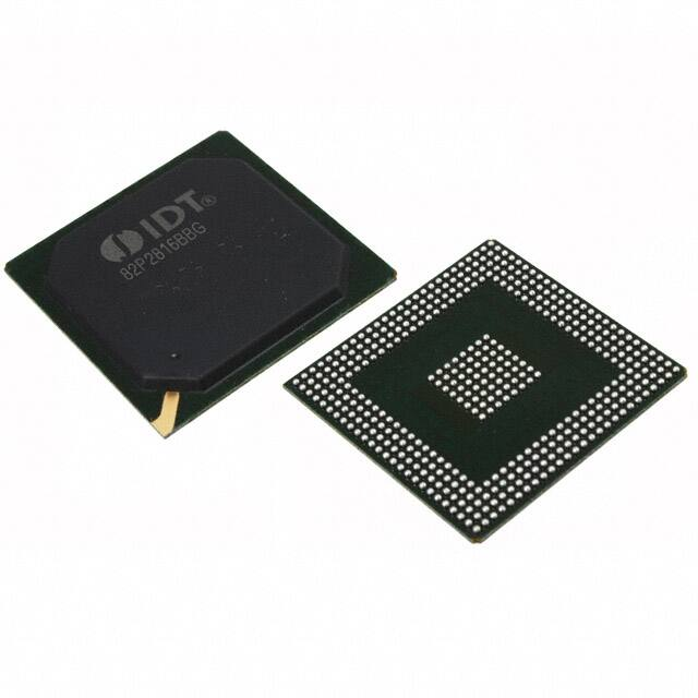
IDT82P2816
Version 3
February 6, 2009
6024 Silver Creek Valley Road, San Jose, California 95138
Telephone: 1-800-345-7015 or 408-284-8200• TWX: 910-338-2070 • FAX: 408-284-2775
Printed in U.S.A.
© 2009 Integrated Device Technology, Inc.
�DISCLAIMER
Integrated Device Technology, Inc. reserves the right to make changes to its products or specifications at any time, without notice, in order to improve design or performance and to supply the best possible product. IDT does not assume any responsibility for use of any circuitry described other than the circuitry embodied in an IDT product. The Company makes no representations that circuitry
described herein is free from patent infringement or other rights of third parties which may result from its use. No license is granted by implication or otherwise under any patent, patent rights or other
rights, of Integrated Device Technology, Inc.
LIFE SUPPORT POLICY
Integrated Device Technology's products are not authorized for use as critical components in life support devices or systems unless a specific written agreement pertaining to such intended use is executed between the manufacturer and an officer of IDT.
1. Life support devices or systems are devices or systems which (a) are intended for surgical implant into the body or (b) support or sustain life and whose failure to perform, when properly used in
accordance with instructions for use provided in the labeling, can be reasonably expected to result in a significant injury to the user.
2. A critical component is any components of a life support device or system whose failure to perform can be reasonably expected to cause the failure of the life support device or system, or to affect its
safety or effectiveness.
�Table of Contents
TABLE OF CONTENTS ........................................................................................................................................................... 3
LIST OF TABLES .................................................................................................................................................................... 7
LIST OF FIGURES ................................................................................................................................................................... 8
FEATURES ............................................................................................................................................................................. 10
APPLICATIONS...................................................................................................................................................................... 11
DESCRIPTION........................................................................................................................................................................ 11
BLOCK DIAGRAM ................................................................................................................................................................. 12
1 PIN ASSIGNMENT .......................................................................................................................................................... 13
2 PIN DESCRIPTION ......................................................................................................................................................... 14
3 FUNCTIONAL DESCRIPTION ........................................................................................................................................ 24
3.1 T1 / E1 / J1 MODE SELECTION .............................................................................................................................. 24
3.2 RECEIVE PATH ....................................................................................................................................................... 24
3.2.1 Rx Termination ............................................................................................................................................ 24
3.2.1.1 Receive Differential Mode ........................................................................................................... 24
3.2.1.2 Receive Single Ended Mode ....................................................................................................... 26
3.2.2 Equalizer ..................................................................................................................................................... 27
3.2.2.1 Line Monitor ................................................................................................................................ 27
3.2.2.2 Receive Sensitivity ...................................................................................................................... 27
3.2.3 Slicer ........................................................................................................................................................... 28
3.2.4 Rx Clock & Data Recovery ......................................................................................................................... 28
3.2.5 Decoder ...................................................................................................................................................... 28
3.2.6 Receive System Interface ........................................................................................................................... 28
3.2.7 Receiver Power Down ................................................................................................................................ 29
3.3 TRANSMIT PATH .................................................................................................................................................... 29
3.3.1 Transmit System Interface .......................................................................................................................... 29
3.3.2 Tx Clock Recovery ...................................................................................................................................... 30
3.3.3 Encoder ....................................................................................................................................................... 30
3.3.4 Waveform Shaper ....................................................................................................................................... 30
3.3.4.1 Preset Waveform Template ........................................................................................................ 30
3.3.4.2 User-Programmable Arbitrary Waveform .................................................................................... 32
3.3.5 Line Driver ................................................................................................................................................... 34
3.3.5.1 Transmit Over Current Protection ............................................................................................... 34
3.3.6 Tx Termination ............................................................................................................................................ 34
3.3.6.1 Transmit Differential Mode .......................................................................................................... 34
3.3.6.2 Transmit Single Ended Mode ...................................................................................................... 35
3.3.7 Transmitter Power Down ............................................................................................................................ 36
3.3.8 Output High-Z on TTIP and TRING ............................................................................................................ 36
3.4 JITTER ATTENUATOR (RJA & TJA) ....................................................................................................................... 37
Table of Contents
3
February 6, 2009
�IDT82P2816
16(+1) CHANNEL HIGH-DENSITY T1/E1/J1 LINE INTERFACE UNIT
3.5 DIAGNOSTIC FACILITIES .......................................................................................................................................
3.5.1 Bipolar Violation (BPV) / Code Violation (CV) Detection and BPV Insertion ..............................................
3.5.1.1 Bipolar Violation (BPV) / Code Violation (CV) Detection .............................................................
3.5.1.2 Bipolar Violation (BPV) Insertion .................................................................................................
3.5.2 Excessive Zeroes (EXZ) Detection .............................................................................................................
3.5.3 Loss of Signal (LOS) Detection ...................................................................................................................
3.5.3.1 Line LOS (LLOS) .........................................................................................................................
3.5.3.2 System LOS (SLOS) ...................................................................................................................
3.5.3.3 Transmit LOS (TLOS) .................................................................................................................
3.5.4 Alarm Indication Signal (AIS) Detection and Generation ............................................................................
3.5.4.1 Alarm Indication Signal (AIS) Detection ......................................................................................
3.5.4.2 (Alarm Indication Signal) AIS Generation ...................................................................................
3.5.5 PRBS, QRSS, ARB and IB Pattern Generation and Detection ...................................................................
3.5.5.1 Pattern Generation ......................................................................................................................
3.5.5.2 Pattern Detection ........................................................................................................................
3.5.6 Error Counter ..............................................................................................................................................
3.5.6.1 Automatic Error Counter Updating ..............................................................................................
3.5.6.2 Manual Error Counter Updating ..................................................................................................
3.5.7 Receive /Transmit Multiplex Function (RMF / TMF) Indication ...................................................................
3.5.7.1 RMFn Indication ..........................................................................................................................
3.5.7.2 TMFn Indication ..........................................................................................................................
3.5.8 Loopback ....................................................................................................................................................
3.5.8.1 Analog Loopback ........................................................................................................................
3.5.8.2 Remote Loopback .......................................................................................................................
3.5.8.3 Digital Loopback ..........................................................................................................................
3.5.8.4 Dual Loopback ............................................................................................................................
3.5.9 Channel 0 Monitoring ..................................................................................................................................
3.5.9.1 G.772 Monitoring .........................................................................................................................
3.5.9.2 Jitter Measurement (JM) .............................................................................................................
3.6 CLOCK INPUTS AND OUTPUTS ............................................................................................................................
3.6.1 Free Running Clock Outputs on CLKT1/CLKE1 .........................................................................................
3.6.2 Clock Outputs on REFA/REFB ...................................................................................................................
3.6.2.1 REFA/REFB in Clock Recovery Mode ........................................................................................
3.6.2.2 Frequency Synthesizer for REFA Clock Output ..........................................................................
3.6.2.3 Free Run Mode for REFA Clock Output ......................................................................................
3.6.2.4 REFA/REFB Driven by External CLKA/CLKB Input ....................................................................
3.6.2.5 REFA and REFB in Loss of Signal (LOS) or Loss of Clock Condition ........................................
3.6.3 MCLK, Master Clock Input ..........................................................................................................................
3.6.4 XCLK, Internal Reference Clock Input ........................................................................................................
3.7 INTERRUPT SUMMARY .........................................................................................................................................
4 MISCELLANEOUS ..........................................................................................................................................................
4.1 RESET .....................................................................................................................................................................
4.1.1 Power-On Reset .........................................................................................................................................
4.1.2 Hardware Reset ..........................................................................................................................................
4.1.3 Global Software Reset ................................................................................................................................
Table of Contents
4
38
38
38
38
38
39
39
40
41
42
42
42
43
43
44
45
45
46
47
47
48
49
49
50
51
52
54
54
55
56
56
57
57
57
57
57
57
61
61
62
64
64
65
65
65
February 6, 2009
�IDT82P2816
5
6
7
8
16(+1) CHANNEL HIGH-DENSITY T1/E1/J1 LINE INTERFACE UNIT
4.1.4 Per-Channel Software Reset ...................................................................................................................... 65
4.2 MICROPROCESSOR INTERFACE ......................................................................................................................... 65
4.3 POWER UP .............................................................................................................................................................. 66
4.4 HITLESS PROTECTION SWITCHING (HPS) SUMMARY ...................................................................................... 66
PROGRAMMING INFORMATION ................................................................................................................................... 69
5.1 REGISTER MAP ...................................................................................................................................................... 69
5.1.1 Global Register ........................................................................................................................................... 69
5.1.2 Per-Channel Register ................................................................................................................................. 70
5.2 REGISTER DESCRIPTION ..................................................................................................................................... 73
5.2.1 Global Register ........................................................................................................................................... 73
5.2.2 Per-Channel Register ................................................................................................................................. 81
JTAG ............................................................................................................................................................................. 113
6.1 JTAG INSTRUCTION REGISTER (IR) .................................................................................................................. 113
6.2 JTAG DATA REGISTER ........................................................................................................................................ 113
6.2.1 Device Identification Register (IDR) .......................................................................................................... 113
6.2.2 Bypass Register (BYP) ............................................................................................................................. 113
6.2.3 Boundary Scan Register (BSR) ................................................................................................................ 113
6.3 TEST ACCESS PORT (TAP) CONTROLLER ....................................................................................................... 113
THERMAL MANAGEMENT .......................................................................................................................................... 115
7.1 JUNCTION TEMPERATURE ................................................................................................................................. 115
7.2 EXAMPLE OF JUNCTION TEMPERATURE CALCULATION ............................................................................... 115
7.3 HEATSINK EVALUATION ..................................................................................................................................... 115
PHYSICAL AND ELECTRICAL SPECIFICATIONS ..................................................................................................... 116
8.1 ABSOLUTE MAXIMUM RATINGS ......................................................................................................................... 116
8.2 RECOMMENDED OPERATING CONDITIONS .................................................................................................... 117
8.3 DEVICE POWER CONSUMPTION AND DISSIPATION (TYPICAL) 1 ................................................................. 118
8.4 DEVICE POWER CONSUMPTION AND DISSIPATION (MAXIMUM) 1 ............................................................... 119
8.5 D.C. CHARACTERISTICS ..................................................................................................................................... 120
8.6 E1 RECEIVER ELECTRICAL CHARACTERISTICS ............................................................................................. 121
8.7 T1/J1 RECEIVER ELECTRICAL CHARACTERISTICS ......................................................................................... 122
8.8 E1 TRANSMITTER ELECTRICAL CHARACTERISTICS ...................................................................................... 123
8.9 T1/J1 TRANSMITTER ELECTRICAL CHARACTERISTICS ................................................................................. 124
8.10 TRANSMITTER AND RECEIVER TIMING CHARACTERISTICS ......................................................................... 125
8.11 CLKE1 TIMING CHARACTERISTICS ................................................................................................................... 127
8.12 JITTER ATTENUATION CHARACTERISTICS ...................................................................................................... 128
8.13 MICROPROCESSOR INTERFACE TIMING ......................................................................................................... 131
8.13.1 Serial Microprocessor Interface ................................................................................................................ 131
8.13.2 Parallel Motorola Non-Multiplexed Microprocessor Interface ................................................................... 133
8.13.2.1 Read Cycle Specification .......................................................................................................... 133
8.13.2.2 Write Cycle Specification .......................................................................................................... 134
8.13.3 Parallel Intel Non-Multiplexed Microprocessor Interface ........................................................................... 135
8.13.3.1 Read Cycle Specification .......................................................................................................... 135
8.13.3.2 Write Cycle Specification .......................................................................................................... 136
Table of Contents
5
February 6, 2009
�IDT82P2816
16(+1) CHANNEL HIGH-DENSITY T1/E1/J1 LINE INTERFACE UNIT
8.13.4 Parallel Motorola Multiplexed Microprocessor Interface ........................................................................... 137
8.13.4.1 Read Cycle Specification .......................................................................................................... 137
8.13.4.2 Write Cycle Specification .......................................................................................................... 138
8.13.5 Parallel Intel Multiplexed Microprocessor Interface .................................................................................. 139
8.13.5.1 Read Cycle Specification .......................................................................................................... 139
8.13.5.2 Write Cycle Specification .......................................................................................................... 140
8.14 JTAG TIMING CHARACTERISTICS ..................................................................................................................... 141
GLOSSARY ......................................................................................................................................................................... 142
INDEX .................................................................................................................................................................................. 144
ORDERING INFORMATION ................................................................................................................................................ 146
Table of Contents
6
February 6, 2009
�List of Tables
Table-1
Table-2
Table-3
Table-4
Table-5
Table-6
Table-7
Table-8
Table-9
Table-10
Table-11
Table-12
Table-13
Table-14
Table-15
Table-16
Table-17
Table-18
Table-19
Table-20
Table-21
Table-22
Table-23
Table-24
Table-25
Table-26
Table-27
Operation Mode Selection ...........................................................................................................................................................................
Impedance Matching Value in Receive Differential Mode ...........................................................................................................................
Multiplex Pin Used in Receive System Interface .........................................................................................................................................
Multiplex Pin Used in Transmit System Interface ........................................................................................................................................
PULS[3:0] Setting in T1/J1 Mode .................................................................................................................................................................
PULS[3:0] Setting in E1 Mode .....................................................................................................................................................................
Transmit Waveform Value for T1 0 ~ 133 ft .................................................................................................................................................
Transmit Waveform Value for T1 133 ~ 266 ft .............................................................................................................................................
Transmit Waveform Value for T1 266 ~ 399 ft .............................................................................................................................................
Transmit Waveform Value for T1 399 ~ 533 ft .............................................................................................................................................
Transmit Waveform Value for T1 533 ~ 655 ft .............................................................................................................................................
Transmit Waveform Value for E1 75 ohm ....................................................................................................................................................
Transmit Waveform Value for E1 120 ohm ..................................................................................................................................................
Transmit Waveform Value for J1 0 ~ 655 ft .................................................................................................................................................
Impedance Matching Value in Transmit Differential Mode ..........................................................................................................................
EXZ Definition ..............................................................................................................................................................................................
LLOS Criteria ...............................................................................................................................................................................................
SLOS Criteria ...............................................................................................................................................................................................
TLOS Detection Between Two Channels ....................................................................................................................................................
AIS Criteria ...................................................................................................................................................................................................
RMFn Indication ...........................................................................................................................................................................................
TMFn Indication ...........................................................................................................................................................................................
Clock Output on CLKT1 ...............................................................................................................................................................................
Clock Output on CLKE1 ...............................................................................................................................................................................
Interrupt Summary .......................................................................................................................................................................................
After Reset Effect Summary ........................................................................................................................................................................
Microprocessor Interface .............................................................................................................................................................................
List of Tables
7
24
25
28
30
31
31
33
33
33
33
33
33
33
33
34
38
39
40
41
42
47
48
56
56
62
64
65
February 6, 2009
�List of Figures
Figure-1
Figure-2
Figure-3
Figure-4
Figure-5
Figure-6
Figure-7
Figure-8
Figure-9
Figure-10
Figure-11
Figure-12
Figure-13
Figure-14
Figure-15
Figure-16
Figure-17
Figure-18
Figure-19
Figure-20
Figure-21
Figure-22
Figure-23
Figure-24
Figure-25
Figure-26
Figure-27
Figure-28
Figure-29
Figure-30
Figure-31
Figure-32
Figure-33
Figure-34
Figure-35
Figure-36
Figure-37
Figure-38
Figure-39
Figure-40
Figure-41
Figure-42
Figure-43
Figure-44
Figure-45
Figure-46
Figure-47
Figure-48
Functional Block Diagram ............................................................................................................................................................................ 12
416-Pin PBGA (Top View) ........................................................................................................................................................................... 13
Switch between Impedance Matching Modes .............................................................................................................................................. 24
Receive Differential Line Interface with Twisted Pair Cable (with transformer) ........................................................................................... 25
Receive Differential Line Interface with Coaxial Cable (with transformer) ................................................................................................... 25
Receive Differential Line Interface with Twisted Pair Cable (transformer-less, non standard compliant) .................................................... 26
Receive Single Ended Line Interface with Coaxial Cable (with transformer) ............................................................................................... 26
Receive Single Ended Line Interface with Coaxial Cable (transformer-less, non standard compliant) ....................................................... 26
Receive Path Monitoring .............................................................................................................................................................................. 27
Transmit Path Monitoring ............................................................................................................................................................................ 27
DSX-1 Waveform Template ........................................................................................................................................................................ 30
T1 Waveform Template Measurement Circuit ............................................................................................................................................. 30
E1 Waveform Template ............................................................................................................................................................................... 31
E1 Waveform Template Measurement Circuit ............................................................................................................................................ 31
Transmit Differential Line Interface with Twisted Pair Cable (with Transformer) ........................................................................................ 35
Transmit Differential Line Interface with Coaxial Cable (with transformer) ................................................................................................. 35
Transmit Differential Line Interface with Twisted Pair Cable (transformer-less, non standard compliant) .................................................. 35
Transmit Single Ended Line Interface with Coaxial Cable (with transformer) ............................................................................................. 35
Jitter Attenuator ........................................................................................................................................................................................... 37
LLOS Indication on Pins .............................................................................................................................................................................. 39
TLOS Detection Between Two Channels .................................................................................................................................................... 41
Pattern Generation (1) ................................................................................................................................................................................. 43
Pattern Generation (2) ................................................................................................................................................................................. 43
PRBS / ARB Detection ................................................................................................................................................................................ 44
IB Detection ................................................................................................................................................................................................. 45
Automatic Error Counter Updating .............................................................................................................................................................. 46
Manual Error Counter Updating .................................................................................................................................................................. 46
Priority Of Diagnostic Facilities During Analog Loopback ........................................................................................................................... 49
Priority Of Diagnostic Facilities During Manual Remote Loopback ............................................................................................................. 50
Priority Of Diagnostic Facilities During Digital Loopback ............................................................................................................................ 51
Priority Of Diagnostic Facilities During Manual Remote Loopback + Manual Digital Loopback ................................................................. 53
Priority Of Diagnostic Facilities During Manual Remote Loopback + Automatic Digital Loopback ............................................................. 53
G.772 Monitoring ......................................................................................................................................................................................... 54
Automatic JM Updating ............................................................................................................................................................................... 55
Manual JM Updating ................................................................................................................................................................................... 55
REFA Output Options in Normal Operation ................................................................................................................................................ 58
REFB Output Options in Normal Operation ................................................................................................................................................ 59
REFA Output in LLOS Condition (When RCLKn Is Selected) ..................................................................................................................... 59
REFA Output in No CLKA Condition (When CLKA Is Selected) ................................................................................................................. 60
Interrupt Service Process ............................................................................................................................................................................ 63
Reset ........................................................................................................................................................................................................... 64
1+1 HPS Scheme, Differential Interface (Shared Common Transformer) .................................................................................................. 66
1:1 HPS Scheme, Differential Interface (Individual Transformer) ............................................................................................................... 67
1+1 HPS Scheme, E1 75 ohm Single-Ended Interface (Shared Common Transformer) ........................................................................... 68
JTAG Architecture ..................................................................................................................................................................................... 113
JTAG State Diagram ................................................................................................................................................................................. 114
Transmit Clock Timing Diagram ................................................................................................................................................................ 126
Receive Clock Timing Diagram ................................................................................................................................................................. 126
List of Figures
8
February 6, 2009
�IDT82P2816
Figure-49
Figure-50
Figure-51
Figure-52
Figure-53
Figure-54
Figure-55
Figure-56
Figure-57
Figure-58
Figure-59
Figure-60
Figure-61
Figure-62
Figure-63
Figure-64
Figure-65
16(+1) CHANNEL HIGH-DENSITY T1/E1/J1 LINE INTERFACE UNIT
CLKE1 Clock Timing Diagram ...................................................................................................................................................................
E1 Jitter Tolerance Performance ...............................................................................................................................................................
T1/J1 Jitter Tolerance Performance ..........................................................................................................................................................
E1 Jitter Transfer Performance .................................................................................................................................................................
T1/J1 Jitter Transfer Performance .............................................................................................................................................................
Read Operation in Serial Microprocessor Interface ..................................................................................................................................
Write Operation in Serial Microprocessor Interface ...................................................................................................................................
Timing Diagram .........................................................................................................................................................................................
Parallel Motorola Non-Multiplexed Microprocessor Interface Read Cycle ................................................................................................
Parallel Motorola Non-Multiplexed Microprocessor Interface Write Cycle ................................................................................................
Parallel Intel Non-Multiplexed Microprocessor Interface Read Cycle .......................................................................................................
Parallel Intel Non-Multiplexed Microprocessor Interface Write Cycle ........................................................................................................
Parallel Motorola Multiplexed Microprocessor Interface Read Cycle ........................................................................................................
Parallel Motorola Multiplexed Microprocessor Interface Write Cycle ........................................................................................................
Parallel Intel Multiplexed Microprocessor Interface Read Cycle ...............................................................................................................
Parallel Intel Multiplexed Microprocessor Interface Write Cycle ...............................................................................................................
JTAG Timing .............................................................................................................................................................................................
List of Figures
9
127
129
129
130
130
131
131
132
133
134
135
136
137
138
139
140
141
February 6, 2009
�16(+1) Channel
High-Density T1/E1/J1
Line Interface Unit
IDT82P2816
FEATURES
Integrates 16+1 channels T1/E1/J1 short haul line interface
units for 100 Ω T1, 120 Ω E1, 110 Ω J1 twisted pair cable and
75 Ω E1 coaxial cable applications
Per-channel configurable Line Interface options
• Supports various line interface options
– Differential and Single Ended line interfaces
– true Single Ended termination on primary and secondary side of trans-
– transformer-less for Differential interfaces
• Fully integrated and software selectable receive and transmit
termination
– Option 1: Fully Internal Impedance Matching with integrated receive
former for E1 75 Ω coaxial cable applications
termination resistor
– Option 2: Partially Internal Impedance Matching with common external
resistor for improved device power dissipation
– Option 3: External impedance Matching termination
• Supports global configuration and per-channel configuration to
T1, E1 or J1 mode
Per-channel programmable features
• Provides T1/E1/J1 short haul waveform templates and userprogrammable arbitrary waveform templates
• Provides two JAs (Jitter Attenuator) for each channel of receiver
and transmitter
• Supports AMI/B8ZS (for T1/J1) and AMI/HDB3 (for E1) encoding
and decoding
Per-channel System Interface options
• Supports Single Rail, Dual Rail with clock or without clock and
sliced system interface
• Integrated Clock Recovery for the transmit interface to recover
transmit clock from system transmit data
Per-channel system and diagnostic functions
• Provides transmit driver over-current detection and protection
with optional automatic high impedance of transmit interface
• Detects and generates PRBS (Pseudo Random Bit Sequence),
ARB (Arbitrary Pattern) and IB (Inband Loopback) in either
receive or transmit direction
• Provides defect and alarm detection in both receive and transmit
directions.
– Defects include BPV (Bipolar Violation) /CV (Code Violation) and EXZ
(Excessive Zeroes)
– Alarms include LLOS (Line LOS), SLOS (System LOS), TLOS
(Transmit LOS) and AIS (Alarm Indication Signal)
• Programmable LLOS detection /clear levels. Compliant with ITU
and ANSI specifications
• Various pattern, defect and alarm reporting options
– Serial hardware LLOS reporting (LLOS, LLOS0) for all 17 channels
– Configurable per-channel hardware reporting with RMF/TMF
(Receive /Transmit Multiplex Function)
– Register access to individual registers or 16-bit error counters
• Supports Analog Loopback, Digital Loopback and Remote
Loopback
• Supports T1.102 line monitor
Channel 0 monitoring options
• Channel 0 can be configured as monitoring channel or regular
channel to increase capacity
• Supports all internal G.772 Monitoring for Non-Intrusive
Monitoring of any of the 16 channels of receiver or transmitter
• Jitter Measurement per ITU O.171
Hitless Protection Switching (HPS) without external Relays
• Supports 1+1 and 1:1 hitless protection switching
• Asynchronous hardware control (OE, RIM) for fast global high
impedance of receiver and transmitter (hot switching between
working and backup board)
• High impedance transmitter and receiver while powered down
• Per-channel register control for high impedance, independent for
receiver and transmitter
Clock Inputs and Outputs
• Flexible master clock (N x 1.544 MHz or N x 2.048 MHz) (1 ≤ N ≤
8, N is an integer number)
• Two selectable reference clock outputs
– from the recovered clock of any of the 17 channels
– from external clock input
– from device master clock
• Integrated clock synthesizer can multiply or divide the reference
clock to a wide range of frequencies: 8 KHz, 64 KHz, 2.048 MHz,
4.096 MHz, 8.192 MHz, 19.44 MHz and 32.768 MHz
• Cascading is provided to select a single reference clock from
multiple devices without the need for any external logic
Microprocessor Interface
• Supports Serial microprocessor interface and Parallel Intel /
Motorola Non-Multiplexed /Multiplexed microprocessor interface
Other Key Features
• IEEE1149.1 JTAG boundary scan
• Two general purpose I/O pins
• 3.3 V I/O with 5 V tolerant inputs
• 3.3 V and 1.8 V power supply
• Package: 416-pin PBGA (27 mm X 27 mm)
Applicable Standards
• AT&T Pub 62411 Accunet T1.5 Service
• ANSI T1.102, T1.403 and T1.231
• Bellcore TR-TSY-000009, GR-253-CORE and GR-499-CORE
• ETSI CTR12/13
• ETS 300166 and ETS 300 233
• G.703, G.735, G.736, G.742, G.772, G.775, G.783 and G.823
• O.161
• ITU I.431 and ITU O.171
IDT and the IDT logo are trademarks of Integrated Device Technology, Inc.
10
2009 Integrated Device Technology, Inc.
February 6, 2009
DSC-6250/3
�IDT82P2816
16(+1) CHANNEL HIGH-DENSITY T1/E1/J1 LINE INTERFACE UNIT
APPLICATIONS
DESCRIPTION
In the transmit path, the data to be transmitted is input on TDn in
Single Rail NRZ Format mode or TDPn/TDNn in Dual Rail NRZ Format
mode and Dual Rail RZ Format mode, and is sampled by a transmit
reference clock. The clock can be supplied externally from TCLKn or
recovered from the input transmit data by an internal Clock Recovery. A
selectable JA in Tx path is used to de-jitter gapped clocks. To meet T1/
E1/J1 waveform standards, five preset T1 templates and two E1
templates, as well as an arbitrary waveform generator are provided. The
data through the Waveform Shaper, the Line Driver and the Tx Transmitter is output on TTIPn and TRINGn.
The IDT82P2816 is a 16+1 channels high-density T1/E1/J1 short
haul Line Interface Unit. Each channel of the IDT82P2816 can be independently configured. The configuration is performed through a Serial or
Parallel Intel/Motorola Non-Multiplexed /Multiplexed microprocessor
interface.
Alarms (including LOS, AIS) and defects (including BPV, EXZ) are
detected in both receive line side and transmit system side. AIS alarm,
PRBS, ARB and IB patterns can be generated /detected in receive /
transmit direction for testing purpose. Analog Loopback, Digital Loopback and Remote Loopback are all integrated for diagnostics.
In the receive path, through a Single Ended or Differential line interface, the received signal is processed by an adaptive Equalizer and then
sent to a Slicer. Clock and data are recovered from the digital pulses
output from the Slicer. After passing through an enabled or disabled
Receive Jitter Attenuator, the recovered data is decoded using B8ZS/
AMI/HDB3 line code rule in Single Rail NRZ Format mode and output to
the system, or output to the system without decoding in Dual Rail NRZ
Format mode and Dual Rail RZ Format mode.
Channel 0 is a special channel. Besides normal operation as the
other 16 channels, channel 0 also supports G.772 Monitoring and Jitter
Measurement per ITU O.171.
SDH/SONET multiplexers
Central office or PBX (Private Branch Exchange)
Digital access cross connects
Remote wireless modules
Microwave transmission systems
Applications
A line monitor function per T1.102 is available to provide a Non-Intrusive Monitoring of channels of other devices.
JTAG per IEEE 1149.1 is also supported by the IDT82P2816.
11
February 6, 2009
�Block Diagram
TRING[16:0]
TTIP[16:0]
RRING[16:0]
RTIP[16:0]
12
Waveform
Shaper
Line
Driver
Defect/Alarm
Detector
Tx Clock
Recovery
JTAG
RCLK[16:0]
Encoder
Pattern
Generator/
Detector
Decoder
Clock Generator
TJA
RJA
Digital Loopback
Remote Loopback
Rx Clock &
Data
Recovery
CLKB
CLKA
REFB
REFA
CLKE1
CLKT1
MCKSEL[3:0]
MCLK
MCU Interface
Alarm
Generator
Slicer
Amplifier
TDO
TDI
TCK
TMS
TRST
A[10:0]
D[7:0]
SDO/ACK /READY
SDI/R/ W/ WR
SCLK/ DS/RD
ALE/AS
IM
INT/ MOT
P/S
CS
INT
Common Control
G.772
Monitor
Tx
Terminator
Analog
Loopback
Rx
Terminator
Defect/Alarm
Detector
VDDIO
VDDA
VDDD
VDDR
VDDT
GNDA
GNDD
GNDT
TCLK[16:0]/TDN[16:0]
TDN[16:0]/TMF[16:0]
TD[16:0]/TDP[16:0]
RCLK[16:0]/RMF[16:0]
RDN[16:0]/RMF[16:0]
RD[16:0]/RDP[16:0]
LLOS
LLOS0
IDT82P2816
16(+1) CHANNEL HIGH-DENSITY T1/E1/J1 LINE INTERFACE UNIT
BLOCK DIAGRAM
RST
GPIO[1:0]
TEHW
TEHWE
OE
RIM
REF
VCOM[1:0]
VCOMEN
Figure-1 Functional Block Diagram
February 6, 2009
�IDT82P2816
1
PIN ASSIGNMENT
1
A
B
C
16(+1) CHANNEL HIGH-DENSITY T1/E1/J1 LINE INTERFACE UNIT
GNDA
GNDA
VDDA
2
GNDA
GNDA
VDDA
3
TTIP14
GNDT
RTIP14
4
TRING
14
GNDT
RRING
14
5
TTIP13
VDDT
14
6
TRING
13
VDDT
13
VDDR
14
VDDR
13
RTIP13
RRING
13
7
8
9
10
RCLK
TCLK16
VDDIO
16
/TDN16
/RMF16
VDDIO
VDDIO
11
RCLK
RD15/
15
RDP15
/RMF15
12
RD14/
RDP14
13
TD13/
TDP13
14
RD16/
RDP16
TDN15/
TMF15
VDDIO
TD15/
TDP15
16
17
18
19
20
21
22
23
24
25
26
TD10/
TDP10
RD10/
RDP10
TDN9/
TMF9
RDN9/
RMF9
REF
TRING
12
TTIP12
GNDA
GNDA
A
RCLK
RDN12/ TDN11/
TCLK10
11
RMF12 TMF11
/TDN10
/RMF11
TD9/
TDP9
RD9/
RDP9
RCLK9/
RMF9
VDDT
12
VDDT
11
GNDA
GNDA
B
NC
RRING
12
RTIP12
VDDA
VDDA
C
VDDIO
VDDR
12
VDDR
11
VDDA
VDDA
D
RCLK
RDN13/ TDN12/
TCLK11
12
RMF13 TMF12
/TDN11
/RMF12
RCLK
TDN16/ RDN16/ TCLK15 RDN15/ TCLK14
RD13/
14
TMF16 RMF16 /TDN15 RMF15 /TDN14
RDP13
/RMF14
TD16/
TDP16
15
TD12/
TDP12
VDDD
RCLK
TDN14/ RDN14/ TCLK13
RD12/
13
TMF14 RMF14 /TDN13
RDP12
/RMF13
VDDD
TD14/
TDP14
TDN13/
TMF13
TCLK12
/TDN12
TD11/
TDP11
RCLK
RDN11/ TDN10/
TCLK9/
10
RMF11 TMF10
TDN9
/RMF10
VDDD
RD11/
RDP11
RDN10/
RMF10
D
VDDA
VDDA
GNDT
GNDA
E
TRING
15
VDDT
15
VDDR
15
RRING
15
GNDA
RRING
11
GNDT
TRING
11
E
F
TTIP15
VDDT
16
VDDR
16
RTIP15
GNDA
RTIP11
GNDT
TTIP11
F
G
TRING
16
GNDT
RRING
16
GNDA
RRING
10
VDDR
10
VDDT
10
TRING
10
G
H
TTIP16
GNDT
RTIP16
GNDA
RTIP10 VDDR9
VDDT9
TTIP10
H
J
TRING
0
VDDT0
VDDR0
RRING
0
GNDA
RRING
9
GNDT
TRING
9
J
K
TTIP0
VDDT1
VDDR1
RTIP0
GNDD
GNDD
GNDD
GNDD
GNDD
GNDD
GNDD
GNDD
GNDA
RTIP9
GNDT
TTIP9
K
L
TRING
1
GNDT
RRING
1
GNDA
GNDD
GNDD
GNDD
GNDD
GNDD
GNDD
GNDD
GNDD
RRING
8
VDDR8
VDDT8
TRING
8
L
M
TTIP1
GNDT
RTIP1
GNDA
GNDD
GNDD
GNDD
GNDD
GNDD
GNDD
GNDD
GNDD
RTIP8
VDDR7
VDDT7
TTIP8
M
N
TRING
2
VDDT2
VDDR2
RRING
2
GNDD
GNDD
GNDD
GNDD
GNDD
GNDD
GNDD
GNDD
GNDA
RRING
7
GNDT
TRING
7
N
P
TTIP2
VDDT3
VDDR3
RTIP2
GNDD
GNDD
GNDD
GNDD
GNDD
GNDD
GNDD
GNDD
GNDA
RTIP7
GNDT
TTIP7
P
R
TRING
3
GNDT
RRING
3
GNDA
GNDD
GNDD
GNDD
GNDD
GNDD
GNDD
GNDD
GNDD
RRING
6
VDDR6
VDDT6
TRING
6
R
T
TTIP3
GNDT
RTIP3
GNDA
GNDD
GNDD
GNDD
GNDD
GNDD
GNDD
GNDD
GNDD
RTIP6
VDDR5
VDDT5
TTIP6
T
U
TRING
4
VDDT4
VDDR4
RRING
4
GNDD
GNDD
GNDD
GNDD
GNDD
GNDD
GNDD
GNDD
GNDA
RRING
5
GNDT
TRING
5
U
V
TTIP4
GNDA
GNDA
RTIP4
GNDA
RTIP5
GNDT
TTIP5
V
W
VDDA
VDDA
VCOM0
VCOM
EN
VDDIO
VCOM1
VDDA
VDDA
W
Y
TD1/
TDP1
TDN1/
TMF1
TCLK1/
TDN1
RD1/
RDP1
RCLK8/
RMF8
RDN8/
RMF8
RD8/
RDP8
TCLK8/
TDN8
Y
AA
RDN1/
RMF1
RCLK1/
RMF1
TD2/
TDP2
VDDIO
VDDIO
TDN8/
TMF8
TD8/
TDP8
RCLK7/
RMF7
AA
AB
TDN2/
TMF2
TCLK2/
TDN2
RD2/
RDP2
RDN2/
RMF2
RDN7/
RMF7
RD7/
RDP7
TCLK7/
TDN7
TDN7/
TMF7
AB
AC
RCLK2/
RMF2
TD3/
TDP3
TDN3/
TMF3
VDDIO
VDDD
TD7/
TDP7
RCLK6/
RMF6
RDN6/
RMF6
AC
AD
TCLK3/
TDN3
RD3/
RDP3
TD4/
TDP4
RD4/
RDP4
VDDIO
VDDIO
VDDD
VDDD
VDDIO
VDDIO
VDDD
RDN0/
RMF0
VDDD
GPIO1
VDDD
TEHW
VDDIO
D1
VDDIO
A5
VDDIO
P/S
IM
VDDD
LLOS0
VDDD
CLKT1
MCK
SEL3
TD0/
TDP0
RD0/
RDP0
TMS
TDO
GPIO0
TEHWE
D5
D2
A9
A6
A2
INT/
MOT
ALE/AS
CS
LLOS
CLKE1
MCK
SEL1
MCK
SEL2
RDN5/
RMF5
RD6/
RDP6
TCLK6/
TDN6
TDN6/
TMF6
AD
SCLK/
DS/RD
REFA
CLKA
MCK
SEL0
TDN5/
TMF5
RD5/
RDP5
TD6/
TDP6
GNDA
GNDA
AE
INT
REFB
CLKB
MCLK
TD5/
TDP5
TCLK5/ RCLK5/
TDN5
RMF5
GNDA
GNDA
AF
18
19
20
21
22
25
26
AE
GNDA
GNDA
RCLK3/ TCLK4/ RCLK4/ TCLK0/
RMF3
TDN4
RMF4
TDN0
AF
GNDA
GNDA
RDN3/
RMF3
TDN4/
TMF4
RDN4/
RMF4
1
2
3
4
5
TRST
TCK
RIM
IC
D6
D3
A10
A7
A3
A0
TDN0/
TMF0
RCLK0/
RMF0
TDI
OE
RST
D7
D4
D0
A8
A4
A1
6
7
8
9
10
11
12
13
14
15
16
SDO/
ACK/
RDY
SDI/
R/W/
WR
17
23
24
Figure-2 416-Pin PBGA (Top View)
Pin Assignment
13
February 6, 2009
�IDT82P2816
2
16(+1) CHANNEL HIGH-DENSITY T1/E1/J1 LINE INTERFACE UNIT
PIN DESCRIPTION
Name
I/O
Pin No. 1
Description
Line Interface
RTIPn
Input
K4, M3, P4, T3, V4, V24, T23, P24, RTIPn / RRINGn: Receive Bipolar Tip/Ring for Channel 0 ~ 16
M23, K24, H23, F24, C24, D5, C3, The receive line interface supports both Receive Differential mode and Receive Single Ended
F4, H3
mode.
In Receive Differential mode, the received signal is coupled into RTIPn and RRINGn via a 1:1
J4, L3, N4, R3, U4, U24, R23, N24, transformer or without a transformer (transformer-less).
L23, J24, G23, E24, C23, D6, C4, In Receive Single Ended mode, RRINGn should be left open. The received signal is input on
E4, G3
RTIPn via a 2:1 (step down) transformer or without a transformer (transformer-less).
These pins will become High-Z globally or channel specific in the following conditions:
• Global High-Z:
- Connecting the RIM pin to low;
- Loss of MCLK
- During and after power-on reset, hardware reset or global software reset;
• Per-channel High-Z
- Receiver power down by writing ‘1’ to the R_OFF bit (b5, RCF0,...)
Output
K1, M1, P1, T1, V1, V26, T26, P26, TTIPn / TRINGn: Transmit Bipolar Tip /Ring for Channel 0 ~ 16
M26, K26, H26, F26, A24, A5, A3, The transmit line interface supports both Transmit Differential mode and Transmit Single
F1, H1
Ended mode.
In Transmit Differential mode, TTIPn outputs a positive differential pulse while TRINGn outJ1, L1, N1, R1, U1, U26, R26, N26, puts a negative differential pulse. The pulses are coupled to the line side via a 1:2 (step up)
L26, J26, G26, E26, A23, A6, A4, transformer or without a transformer (transformer-less).
E1, G1
In Transmit Single Ended mode, TRINGn should be left open (it is shorted to ground internally). The signal presented at TTIPn is output to the line side via a 1:2 (step up) transformer.
These pins will become High-Z globally or channel specific in the following conditions:
• Global High-Z:
- Connecting the OE pin to low;
- Loss of MCLK;
- During and after power-on reset, hardware reset or global software reset;
• Per-channel High-Z
- Writing ‘0’ to the OE bit (b6, TCF0,...) 2;
- Loss of TCLKn in Transmit Single Rail NRZ Format mode or Transmit Dual Rail NRZ
Format mode, except that the channel is in Remote Loopback or transmit internal pattern with XCLK 3;
- Transmitter power down by writing ‘1’ to the T_OFF bit (b5, TCF0,...);
- Per-channel software reset;
- The THZ_OC bit (b4, TCF0,...) is set to ‘1’ and the transmit driver over-current is
detected.
Refer to Section 3.3.8 Output High-Z on TTIP and TRING for details.
RRINGn
(n=0~16)
TTIPn
TRINGn
(n=0~16)
Note:
1. The pin number of the pins with the footnote ‘n’ is listed in order of channel (CH0 ~ CH16).
2. The content in the brackets indicates the position and the register name of the preceding bit. After the register name, if the punctuation ‘,...’ is followed, this bit is in a per-channel register.
If there is no punctuation following the address, this bit is in a global register or in a channel 0 only register. The addresses and details are included in Chapter 5 Programming Information.
3. XCLK is derived from MCLK. It is 1.544 MHz in T1/J1 mode or 2.048 MHz in E1 mode.
Pin Description
14
February 6, 2009
�IDT82P2816
Name
16(+1) CHANNEL HIGH-DENSITY T1/E1/J1 LINE INTERFACE UNIT
I/O
Pin No.
Description
System Interface
RDn / RDPn
Output
(n=0~16)
AD6, Y4, AB3, AD2, AD4, AE23, RDn: Receive Data for Channel 0 ~ 16
AD24, AB24, Y25, B21, A19, D18, When the receive system interface is configured to Single Rail NRZ Format mode, this multiC16, B14, A12, A10, C9
plex pin is used as RDn.
The decoded NRZ data is updated on the active edge of RCLKn. The active level on RDn is
selected by the RD_INV bit (b3, RCF1,...).
When the receiver is powered down, RDn will be in High-Z state or low, as selected by the
RHZ bit (b6, RCF0,...).
RDPn: Positive Receive Data for Channel 0 ~ 16
When the receive system interface is configured to Dual Rail NRZ Format mode, Dual Rail RZ
Format mode or Dual Rail Sliced mode, this multiplex pin is used as RDPn.
In Receive Dual Rail NRZ Format mode, the un-decoded NRZ data is output on RDPn and
RDNn and updated on the active edge of RCLKn.
In Receive Dual Rail RZ Format mode, the un-decoded RZ data is output on RDPn and RDNn
and updated on the active edge of RCLKn.
In Receive Dual Rail Sliced mode, the raw RZ sliced data is output on RDPn and RDNn.
For Receive Differential line interface, an active level on RDPn indicates the receipt of a positive pulse on RTIPn and a negative pulse on RRINGn; while an active level on RDNn indicates the receipt of a negative pulse on RTIPn and a positive pulse on RRINGn.
For Receive Single Ended line interface, an active level on RDPn indicates the receipt of a
positive pulse on RTIPn; while an active level on RDNn indicates the receipt of a negative
pulse on RTIPn.
The active level on RDPn and RDNn is selected by the RD_INV bit (b3, RCF1,...).
When the receiver is powered down, RDPn and RDNn will be in High-Z state or low, as
selected by the RHZ bit (b6, RCF0,...).
RDNn / RMFn
(n=0~16)
Output
AC6, AA1, AB4, AF3, AF5, AD23, RDNn: Negative Receive Data for Channel 0 ~ 16
AC26, AB23, Y24, A21, D20, C18, When the receive system interface is configured to Dual Rail NRZ Format mode, Dual Rail RZ
B16, A14, C13, B11, B9
Format mode or Dual Rail Sliced mode, this multiplex pin is used as RDNn.
(Refer to the description of RDPn for details).
RMFn: Receive Multiplex Function for Channel 0 ~ 16
When the receive system interface is configured to Single Rail NRZ Format mode, this multiplex pin is used as RMFn.
RMFn is configured by the RMF_DEF[2:0] bits (b7~5, RCF1,...) and can indicate PRBS/ARB,
LAIS, LEXZ, LBPV, LEXZ+LBPV, LLOS, output recovered clock (RCLK) or XOR output of
positive and negative sliced data. Refer to Section 3.5.7.1 RMFn Indication for details.
The output on RMFn is updated on the active edge of RCLKn. The active level of RMFn is
always high.
When the receiver is powered down, RMFn will be in High-Z state or low, as selected by the
RHZ bit (b6, RCF0,...).
Pin Description
15
February 6, 2009
�IDT82P2816
16(+1) CHANNEL HIGH-DENSITY T1/E1/J1 LINE INTERFACE UNIT
Name
I/O
RCLKn / RMFn
Output
(n=0~16)
Pin No.
Description
AF7, AA2, AC1, AE3, AE5, AF24, RCLKn: Receive Clock for Channel 0 ~ 16
AC25, AA26, Y23, B22, C20, B18, When the receive system interface is configured to Single Rail NRZ Format mode, Dual Rail
A16, C15, B13, A11, A9
NRZ Format mode or Dual Rail RZ Format mode, this multiplex pin is used as RCLKn.
RCLKn outputs a 1.544 MHz (in T1/J1 mode) or 2.048 MHz (in E1 mode) clock which is
recovered from the received signal.
The data output on RDn and RMFn (in Receive Single Rail NRZ Format mode) or RDPn/
RDNn (in Receive Dual Rail NRZ Format mode, Receive Dual Rail RZ Format mode and
Receive Dual Rail Sliced) is updated on the active edge of RCLKn. The active edge is
selected by the RCK_ES bit (b4, RCF1,...).
In LLOS condition, RCLKn output high or XCLK, as selected by the RCKH bit (b7,
RCF0,...) (refer to Section 3.5.3.1 Line LOS (LLOS) for details).
When the receiver is powered down, RCLKn will be in High-Z state or low, as selected by the
RHZ bit (b6, RCF0,...).
RMFn: Receive Multiplex Function for Channel 0 ~ 16
When the receive system interface is configured to Dual Rail Sliced mode, this multiplex pin is
used as RMFn.
(Refer to the description of RMFn of the RDNn/RMFn multiplex pin for details).
LLOS
Output
AD19
LLOS: Receive Line Loss Of Signal
LLOS synchronizes with the output of CLKE1 and can indicate the LLOS (Line LOS) status of
all 17 channels in a serial format.
When the clock output on CLKE1 is enabled, LLOS indicates the LLOS status of the 17 channels in a serial format and repeats every seventeen cycles. Channel 0 is positioned by
LLOS0. Refer to the description of LLOS0 below for details.
LLOS is updated on the rising edge of CLKE1 and is always active high.
When the clock output of CLKE1 is disabled, LLOS will be held in High-Z state.
(Refer to Section 3.5.3.1 Line LOS (LLOS) for details.)
LLOS0
Output
AC19
LLOS0: Receive Line Loss Of Signal for Channel 0
LLOS0 can indicate the position of channel 0 on the LLOS pin.
When the clock output on CLKE1 is enabled, LLOS0 pulses high for one CLKE1 clock cycle to
indicate the position of channel 0 on the LLOS pin. When CLKE1 outputs 8 KHz clock, LLOS0
pulses high for one 8 KHz clock cycle (125 µs) every seventeen 8 KHz clock cycles; when
CLKE1 outputs 2.048 MHz clock, LLOS0 pulses high for one 2.048 MHz clock cycle (488 ns)
every seventeen 2.048 MHz clock cycles. LLOS0 is updated on the rising edge of CLKE1.
When the clock output on CLKE1 is disabled, LLOS0 will be held in High-Z state.
(Refer to Section 3.5.3.1 Line LOS (LLOS) for details.)
Pin Description
16
February 6, 2009
�IDT82P2816
16(+1) CHANNEL HIGH-DENSITY T1/E1/J1 LINE INTERFACE UNIT
Name
I/O
TDn / TDPn
Input
(n=0~16)
Pin No.
Description
AD5, Y1, AA3, AC2, AD3, AF22, TDn: Transmit Data for Channel 0 ~ 16
AE24, AC24, AA25, B20, A18, C17, When the transmit system interface is configured to Single Rail NRZ Format mode, this multiB15, A13, D12, D10, C8
plex pin is used as TDn.
TDn accepts Single Rail NRZ data. The data is sampled into the device on the active edge of
TCLKn.
The active level on TDn is selected by the TD_INV bit (b3, TCF1,...).
TDPn: Positive Transmit Data for Channel 0 ~ 16
When the transmit system interface is configured to Dual Rail NRZ Format mode or Dual Rail
RZ Format mode, this multiplex pin is used as TDPn.
In Transmit Dual Rail NRZ Format mode, the pre-encoded NRZ data is input on TDPn and
TDNn and sampled on the active edge of TCLKn.
In Transmit Dual Rail RZ Format mode, the pre-encoded RZ data is input on TDPn and TDNn.
The line code is as follows (when the TD_INV bit (b3, TCF1,...) is ‘0’):
TDPn
TDNn
Output Pulse on TTIPn Output Pulse on TRINGn *
0
0
Space
Space
0
1
Negative Pulse
Positive Pulse
1
0
Positive Pulse
Negative Pulse
1
1
Space
Space
Note:
* For Transmit Single Ended line interface, TRINGn should be open.
The active level on TDPn and TDNn is selected by the TD_INV bit (b3, TCF1,...).
TDNn / TMFn
Input / Output
(n=0~16)
AF6, Y2, AB1, AC3, AF4, AE22, TDNn: Negative Transmit Data for Channel 0 ~ 16
AD26, AB26, AA24, A20, C19, B17, When the transmit system interface is configured to Dual Rail NRZ Format mode, this multiA15, D14, C12, C10, B8
plex pin is used as TDNn.
(Refer to the description of TDPn for details).
TMFn: Transmit Multiplex Function for Channel 0 ~ 16
When the transmit system interface is configured to Single Rail NRZ Format mode or Dual
Rail RZ Format mode, this multiplex pin is used as TMFn.
TMFn is configured by the TMF_DEF[2:0] bits (b7~5, TCF1,...) and can indicate PRBS/ARB,
SAIS, TOC, TLOS, SEXZ, SBPV, SEXZ+SBPV, SLOS. Refer to Section 3.5.7.2 TMFn Indication for details.
The output on TMFn is updated on the active edge of TCLKn (if available). The active level of
TMFn is always high.
TCLKn / TDNn
(n=0~16)
Input
AE6, Y3, AB2, AD1, AE4, AF23, TCLKn: Transmit Clock for Channel 0 ~ 16
AD25, AB25, Y26, C21, B19, A17, When the transmit system interface is configured to Single Rail NRZ Format mode or Dual
D16, C14, B12, B10, A8
Rail NRZ Format mode, this multiplex pin is used as TCLKn.
TCLKn inputs a 1.544 MHz (in T1/J1 mode) or 2.048 MHz (in E1 mode) clock.
The data input on TDn (in Transmit Single Rail NRZ Format mode) or TDPn/TDNn (in Transmit Dual Rail NRZ Format mode) is sampled on the active edge of TCLKn. The data output on
TMFn (in Transmit Single Rail NRZ Format mode) is updated on the active edge of TCLKn.
The active edge is selected by the TCK_ES bit (b4, TCF1,...).
TDNn: Negative Transmit Data for Channel 0 ~ 16
When the transmit system interface is configured to Dual Rail RZ Format mode, this multiplex
pin is used as TDNn.
(Refer to the description of TDPn for details).
Pin Description
17
February 6, 2009
�IDT82P2816
Name
16(+1) CHANNEL HIGH-DENSITY T1/E1/J1 LINE INTERFACE UNIT
I/O
Pin No.
Description
Clock
MCLK
Input
AF21
MCLK: Master Clock Input
MCLK provides a stable reference timing for the IDT82P2816. MCLK should be a clock with +/
-32 ppm (in T1/J1 mode) or +/-50 ppm (in E1 mode) accuracy. The clock frequency of MCLK
is informed to the device by MCKSEL[3:0].
If MCLK misses (duty cycle is less than 30% for 10 µs) and then recovers, the device will be
reset automatically.
MCKSEL[0]
Input
AE21
MCKSEL[3:0]: Master Clock Selection
These four pins inform the device of the clock frequency input on MCLK:
MCKSEL[1]
AD21
MCKSEL[2]
AD22
MCKSEL[3]
AC22
MCKSEL[3:0]*
Frequency (MHz)
0000
1.544
0001
1.544 X 2
0010
1.544 X 3
0011
1.544 X 4
0100
1.544 X 5
0101
1.544 X 6
0110
1.544 X 7
0111
1.544 X 8
1000
2.048
1001
2.048 X 2
1010
2.048 X 3
1011
2.048 X 4
1100
2.048 X 5
1101
2.048 X 6
1110
2.048 X 7
1111
2.048 X 8
Note:
0: GNDD
1: VDDIO
CLKT1
Output
AC21
CLKT1: 8 KHz / T1 Clock Output
The output on CLKT1 can be enabled or disabled, as determined by the CLKT1_EN bit (b1,
CLKG).
When the output is enabled, CLKT1 outputs an 8 KHz or 1.544 MHz clock, as selected by the
CLKT1 bit (b0, CLKG). The output is locked to MCLK.
When the output is disabled, CLKT1 is in High-Z state.
CLKE1
Output
AD20
CLKE1: 8 KHz / E1 Clock Output
The output on CLKE1 can be enabled or disabled, as determined by the CLKE1_EN bit (b3,
CLKG).
When the output is enabled, CLKE1 outputs an 8 KHz or 2.048 MHz clock, as selected by the
CLKE1 bit (b2, CLKG). The output is locked to MCLK.
When the output is disabled, CLKE1 is in High-Z state.
Pin Description
18
February 6, 2009
�IDT82P2816
16(+1) CHANNEL HIGH-DENSITY T1/E1/J1 LINE INTERFACE UNIT
Name
I/O
Pin No.
Description
REFA
Output
AE19
REFA: Reference Clock Output A
REFA can output three kinds of clocks: a recovered clock of one of the 17 channels, an external clock input on CLKA or a free running clock. The clock frequency is programmable. Refer
to Section 3.6.2 Clock Outputs on REFA/REFB for details.
The output on REFA can also be disabled, as determined by the REFA_EN bit (b6, REFA).
When the output is disabled, REFA is in High-Z state.
REFB
Output
AF19
REFB: Reference Clock Output B
REFB can output a recovered clock of one of the 17 channels, an external clock input on
CLKB or a free running clock. Refer to Section 3.6.2 Clock Outputs on REFA/REFB for
details.
The output on REFB can also be disabled, as determined by the REFB_EN bit (b6, REFB).
When the output is disabled, REFB is in High-Z state.
CLKA
Input
AE20
CLKA: External T1/E1 Clock Input A
External T1/J1 (1.544 MHz) or E1 (2.048 MHz) clock is input on this pin. The CKA_T1E1 bit
(b5, REFA) should be set to match the clock frequency.
When not used, this pin should be connected to GNDD.
CLKB
Input
AF20
CLKB: External T1/E1 Clock Input B
External T1/J1 (1.544 MHz) or E1 (2.048 MHz) clock is input on this pin. The CKB_T1E1 bit
(b5, REFB) should be set to match the clock frequency.
When not used, this pin should be connected to GNDD.
Common Control
VCOM[0]
Output
VCOM[1]
W3
W24
VCOM: Voltage Common Mode [1:0]
These pins are used only when the receive line interface is in Receive Differential mode and
connected without a transformer (transformer-less).
To enable these pins, the VCOMEN pin must be connected high. Refer to Figure-6 for the
connection.
When these pins are not used, they should be left open.
VCOMEN
Input
(Pull-Down)
W4
VCOMEN: Voltage Common Mode Enable
This pin should be connected high only when the receive line interface is in Receive Differential mode and connected without a transformer (transformer-less).
When not used, this pin should be left open.
REF
-
A22
REF: Reference Resistor
An external resistor (10 KΩ, ±1%) is used to connect this pin to ground to provide a standard
reference current for internal circuit. This resistor is required to ensure correct device operation.
RIM
Input
(Pull-Down)
AE9
RIM: Receive Impedance Matching
In Receive Differential mode, when RIM is low, all 17 receivers become High-Z and only external impedance matching is supported. In this case, the per-channel impedance matching configuration bits - the R_TERM[2:0] bits (b2~0, RCF0,...) and the R120IN bit (b4, RCF0,...) - are
ignored.
In Receive Differential mode, when RIM is high, impedance matching is configured on a perchannel basis by the R_TERM[2:0] bits (b2~0, RCF0,...) and the R120IN bit (b4, RCF0,...).
This pin can be used to control the receive impedance state for Hitless Protection applications. Refer to Section 4.4 Hitless Protection Switching (HPS) Summary for details.
In Receive Single Ended mode, this pin should be left open.
Pin Description
19
February 6, 2009
�IDT82P2816
16(+1) CHANNEL HIGH-DENSITY T1/E1/J1 LINE INTERFACE UNIT
Name
I/O
Pin No.
Description
OE
Input
AF9
OE: Output Enable
OE enables or disables all Line Drivers globally.
A high level on this pin enables all Line Drivers while a low level on this pin places all Line
Drivers in High-Z state and independent from related register settings.
Note that the functionality of the internal circuit is not affected by OE.
If this pin is not used, it should be tied to VDDIO.
This pin can be used to control the transmit impedance state for Hitless protection applications. Refer to Section 4.4 Hitless Protection Switching (HPS) Summary for details.
TEHWE
Input
(Pull-Up)
AD10
TEHWE: Hardware T1/J1 or E1 Mode Selection Enable
When this pin is open, the T1/J1 or E1 operation mode is selected by TEHW globally.
When this pin is low, the T1/J1 or E1 operation mode is selected by the T1E1 bit (b0,
CHCF,...) on a per-channel basis.
TEHW
Input
(Pull-Up)
AC10
TEHW: Hardware T1/J1 or E1 Mode Selection
When TEHWE is open, this pin selects the T1/J1 or E1 operation mode globally:
Low - E1 mode;
Open - T1/J1 mode.
When TEHWE is low, the input on this pin is ignored.
GPIO[0]
Output / Input
AD9
GPIO: General Purpose I/O [1:0]
These two pins can be defined as input pins or output pins by the DIR[1:0] bits (b1~0, GPIO)
respectively.
When the pins are input, their polarities are indicated by the LEVEL[1:0] bits (b3~2, GPIO)
respectively.
When the pins are output, their polarities are controlled by the LEVEL[1:0] bits (b3~2, GPIO)
respectively.
GPIO[1]
RST
AC8
Input
AF10
RST: Reset (Active Low)
A low pulse on this pin resets the device. This hardware reset process completes in 2 µs maximum. Refer to Section 4.1 Reset for an overview on reset options.
MCU Interface
INT
Output
AF18
INT: Interrupt Request
This pin indicates interrupt requests for all unmasked interrupt sources.
The output characteristics (open drain or push-pull internally) and the active level are determined by the INT_PIN[1:0] bits (b3~2, GCF).
CS
Input
AD18
CS: Chip Select (Active Low)
This pin must be asserted low to enable the microprocessor interface.
A transition from high to low must occur on this pin for each Read/Write operation and CS
should remain low until the operation is over.
P/S
Input
AC16
P/S: Parallel or Serial Microprocessor Interface Select
P/S selects Serial or Parallel microprocessor interface for the device:
GNDD - Serial microprocessor interface.
VDDIO - Parallel microprocessor interface.
Serial microprocessor interface consists of the CS, SCLK, SDI, SDO pins.
Parallel microprocessor interface consists of the CS, INT/MOT, IM, DS/RD, ALE/AS, R/W/WR,
ACK/RDY, D[7:0], A[10:0] pins.
INT/MOT
Input
(Pull-Up)
AD16
INT/MOT: Intel or Motorola Microprocessor Interface Select
In Parallel microprocessor interface, INT/MOT selects Intel or Motorola microprocessor interface for the device:
GNDD - Parallel Motorola microprocessor interface.
Open - Parallel Intel microprocessor interface.
In Serial microprocessor interface, this pin should be left open.
Pin Description
20
February 6, 2009
�IDT82P2816
16(+1) CHANNEL HIGH-DENSITY T1/E1/J1 LINE INTERFACE UNIT
Name
I/O
Pin No.
Description
IM
Input
(Pull-Up)
AC17
IM: Interface Mode Selection
In Parallel Motorola or Intel microprocessor interface, IM selects multiplexed bus or non-multiplexed bus for the device:
GNDD - Parallel Motorola /Intel Non-Multiplexed microprocessor interface.
Open - Parallel Motorola /Intel Multiplexed microprocessor interface.
In Serial microprocessor interface, this pin should be connected to GNDD.
ALE / AS
Input
AD17
ALE: Address Latch Enable
In Parallel Intel Multiplexed microprocessor interface, this multiplex pin is used as ALE.
The address on A[10:8] and D[7:0] (A[7:0] are ignored) is sampled into the device on the falling edges of ALE.
AS: Address Strobe
In Parallel Motorola Multiplexed microprocessor interface, this multiplex pin is used as AS.
The address on A[10:8] and D[7:0] (A[7:0] are ignored) is latched into the device on the falling
edges of AS.
In Parallel Motorola /Intel Non-Multiplexed microprocessor interface, this pin should be pulled
high.
In Serial microprocessor interface, this pin should be connected to GNDD.
SCLK / DS / RD
Input
AE18
SCLK: Shift Clock
In Serial microprocessor interface, this multiplex pin is used as SCLK.
SCLK inputs the shift clock for the Serial microprocessor interface. Data on SDI is sampled by
the device on the rising edge of SCLK. Data on SDO is updated on the falling edge of SCLK.
DS: Data Strobe (Active Low)
In Parallel Motorola microprocessor interface, this multiplex pin is used as DS.
During a write operation (R/W = 0), data on D[7:0] is sampled into the device. During a read
operation (R/W = 1), data is driven to D[7:0] by the device.
RD: Read Strobe (Active Low)
In Parallel Intel microprocessor interface, this multiplex pin is used as RD.
RD is asserted low by the microprocessor to initiate a read operation. Data is driven to D[7:0]
by the device during the read operation.
SDI / R/W / WR
Input
AF17
SDI: Serial Data Input
In Serial microprocessor interface, this multiplex pin is used as SDI.
Address and data on this pin are serially clocked into the device on the rising edge of SCLK.
R/W: Read / Write Select
In Parallel Motorola microprocessor interface, this multiplex pin is used as R/W.
R/W is asserted low for write operation or high for read operation.
WR: Write Strobe (Active Low)
In Parallel Intel microprocessor interface, this multiplex pin is used as WR.
WR is asserted low by the microprocessor to initiate a write operation. Data on D[7:0] is sampled into the device during a write operation.
Pin Description
21
February 6, 2009
�IDT82P2816
16(+1) CHANNEL HIGH-DENSITY T1/E1/J1 LINE INTERFACE UNIT
Name
I/O
Pin No.
SDO / ACK / RDY
Output
AE17
Description
SDO: Serial Data Output
In Serial microprocessor interface, this multiplex pin is used as SDO.
Data on this pin is serially clocked out of the device on the falling edge of SCLK.
ACK: Acknowledge Output (Active Low)
In Parallel Motorola microprocessor interface, this multiplex pin is used as ACK.
A low level on ACK indicates that valid information on the data bus is ready for a read operation or acknowledges the acceptance of the written data during a write operation.
RDY: Ready Output
In Parallel Intel microprocessor interface, this multiplex pin is used as RDY.
A high level on RDY reports to the microprocessor that a read/write cycle can be completed. A
low level on RDY reports that wait states must be inserted.
D[0]
D[1]
D[2]
D[3]
D[4]
D[5]
D[6]
D[7]
Output / Input
AF13
AC12
AD12
AE12
AF12
AD11
AE11
AF11
D[7:0]: Bi-directional Data Bus
In Parallel Motorola /Intel Non-Multiplexed microprocessor interface, these pins are the bidirectional data bus of the microprocessor interface.
In Parallel Motorola /Intel Multiplexed microprocessor interface, these pins are the multiplexed
bi-directional address /data bus.
In Serial microprocessor interface, these pins should be connected to GNDD.
A[0]
A[1]
A[2]
A[3]
A[4]
A[5]
A[6]
A[7]
A[8]
A[9]
A[10]
Input
AE16
AF16
AD15
AE15
AF15
AC14
AD14
AE14
AF14
AD13
AE13
A[10:0]: Address Bus
In Parallel Motorola /Intel Non-Multiplexed microprocessor interface, these pins are the
address bus of the microprocessor interface.
In Parallel Motorola /Intel Multiplexed microprocessor interface, A[10:8], together with D[7:0],
are the address bus; while A[7:0] should be connected to GNDD.
In Serial microprocessor interface, these pins should be connected to GNDD.
JTAG (per IEEE 1149.1)
TRST
Input
Pull-Down
AE7
TRST: JTAG Test Reset (Active Low)
A low signal on this pin resets the JTAG test port. To ensure deterministic operation of the test
logic, TMS should be held high when the signal on TRST changes from low to high.
This pin may be left unconnected when JTAG is not used.
This pin has an internal pull-down resistor.
TMS
Input
Pull-up
AD7
TMS: JTAG Test Mode Select
The signal on this pin controls the JTAG test performance and is sampled on the rising edge
of TCK. To ensure deterministic operation of the test logic, TMS should be held high when the
signal on TRST changes from low to high.
This pin may be left unconnected when JTAG is not used.
This pin has an internal pull-up resistor.
TCK
Input
AE8
TCK: JTAG Test Clock
The clock for the JTAG test is input on this pin. TDI and TMS are sampled on the rising edge
of TCK and TDO is updated on the falling edge of TCK.
When TCK is idle at low state, all stored-state devices contained in the test logic shall retain
their state indefinitely.
This pin should be connected to GNDD when JTAG is not used.
Pin Description
22
February 6, 2009
�IDT82P2816
16(+1) CHANNEL HIGH-DENSITY T1/E1/J1 LINE INTERFACE UNIT
Name
I/O
Pin No.
Description
TDI
Input
Pull-up
AF8
TDI: JTAG Test Data Input
The test data is input on this pin. It is clocked into the device on the rising edge of TCK. This
pin has an internal pull-up resistor.
This pin may be left unconnected when JTAG is not used.
TDO
Output
AD8
TDO: JTAG Test Data Output
The test data is output on this pin. It is clocked out of the device on the falling edge of TCK.
TDO is a High-Z output signal except during the process of data scanning.
Power & Ground
VDDIO
A7, B7, C7, D7, D8, D9, D19, D21, VDDIO: 3.3 V I/O Power Supply
D22, W23, AA4, AA23, AC4, AC11,
AC13, AC15
VDDA
C1, C2, C25, C26, D1, D2, D25,
D26, W1, W2, W25, W26
VDDA: 3.3 V Analog Core Power Supply
VDDD
C11, D11, D13, D15, D17, AC5,
AC7, AC9, AC18, AC20, AC23
VDDD: 1.8 V Digital Core Power Supply
VDDRn
J3, K3, N3, P3, U3, T24, R24, M24, VDDRn: 3.3 V Power Supply for Receiver
L24, H24, G24, D24, D23, C6, C5,
E3, F3
(N=0~16)
VDDTn
J2, K2, N2, P2, U2, T25, R25, M25, VDDTn: 3.3 V Power Supply for Transmitter Driver
L25, H25, G25, B24, B23, B6, B5,
E2, F2
(N=0~16)
GNDA
A1, A2, A25, A26, B1, B2, B25, GNDA: GND for Analog Core / Receiver
B26, D4, E23, F23, G4, H4, J23,
K23, L4, M4, N23, P23, R4, T4,
U23, V2, V3, V23, AE1, AE2, AE25,
AE26, AF1, AF2, AF25, AF26
GNDD
K10, K11, K12, K13, K14, K15, K16, GNDD: Digital GND
K17, L10, L11, L12, L13, L14, L15,
L16, L17, M10, M11, M12, M13,
M14, M15, M16, M17, N10, N11,
N12, N13, N14, N15, N16, N17,
P10, P11, P12, P13, P14, P15, P16,
P17, R10, R11, R12, R13, R14,
R15, R16, R17, T10, T11, T12, T13,
T14, T15, T16, T17, U10, U11, U12,
U13, U14, U15, U16, U17
GNDT
B3, B4, D3, E25, F25, G2, H2, J25, GNDT: Analog GND for Transmitter Driver
K25, L2, M2, N25, P25, R2, T2,
U25, V25
TEST
IC
-
AE10
IC: Internal Connected
This pin is for IDT use only and should be connected to GNDD.
Others
NC
Pin Description
-
C22
NC: Not Connected
23
February 6, 2009
�IDT82P2816
16(+1) CHANNEL HIGH-DENSITY T1/E1/J1 LINE INTERFACE UNIT
3
FUNCTIONAL DESCRIPTION
3.1
T1 / E1 / J1 MODE SELECTION
The IDT82P2816 can be configured to T1/J1 mode or E1 mode
globally or on a per-channel basis. The configuration is determined by
the TEHWE pin, the TEHW pin and the T1E1 bit (b0, CHCF,...). Refer to
Table-1 for details of the operation mode selection.
Table-1 Operation Mode Selection
TEHWE Pin
TEHW Pin
T1E1 Bit
Operation Mode
Global Programming
Per-Channel Programming
Open
Low
Open
Low
(The configuration of this pin is ignored)
(The configuration of this bit is ignored).
T1/J1
E1
0
1
T1/J1
E1
3.2
RECEIVE PATH
Physical And Electrical Specifications.
3.2.1
RX TERMINATION
External Impedance Matching circuit uses an external resistor (Rr)
only.
The receive line interface supports Receive Differential mode and
Receive Single Ended mode, as selected by the R_SING bit (b3,
RCF0,...). In Receive Differential mode, both RTIPn and RRINGn are
used to receive signal from the line side. In Receive Single Ended mode,
only RTIPn is used to receive signal.
RIM
RTIP
In Receive Differential mode, the line interface can be connected
with T1 100 Ω, J1 110 Ω or E1 120 Ω twisted pair cable or E1 75 Ω
coaxial cable. In Receiver Single Ended mode, the line interface can
only be connected with 75 Ω coaxial cable.
1
0
1
R_TERM2
Receive
path
The receive impedance matching is realized by using internal impedance matching or external impedance matching for each channel in
different applications.
R120IN 1 0
3.2.1.1 Receive Differential Mode
Rr = 120 Ω
In Receive Differential mode, three kinds of impedance matching are
supported: Fully Internal Impedance Matching, Partially Internal Impedance Matching and External Impedance Matching. Figure-3 shows an
overview of how these Impedance Matching modes are switched.
IM
R_TERM[1:0]
RRING
Figure-3 Switch between Impedance Matching Modes
Fully Internal Impedance Matching circuit uses an internal programmable resistor (IM) only and does not use an external resistor. This
configuration saves external components and supports 1:1 Hitless
Protection Switching (HPS) applications without relays. Refer to
Section 4.4 Hitless Protection Switching (HPS) Summary.
To support some particular applications, such as hot-swap or Hitless
Protection Switch (HPS) hot-switchover, RTIPn/RRINGn must be forced
to enter high impedance state (i.e., External Impedance Matching). For
hot-swap, RTIPn/RRINGn must be always held in high impedance state
during /after power up; for HPS hot-switchover, RTIPn/RRINGn must
enter high impedance state immediately after switchover. Though each
channel can be individually configured to External Impedance Matching
through register access, it is too slow for hitless switch. Therefore, a
hardware pin - RIM - is provided to globally control the high impedance
for all 17 receivers.
Partially Internal Impedance Matching circuit consists of an internal
programmable resistor (IM) and a value-fixed 120 Ω external resistor
(Rr). Compared with Fully Internal Impedance Matching, this configuration provides considerable savings in power dissipation of the device.
For example, In E1 120 Ω PRBS mode, the power savings would be
0.44 W. For power savings in other modes, please refer to Chapter 8
Functional Description
0
RIN
24
February 6, 2009
�IDT82P2816
16(+1) CHANNEL HIGH-DENSITY T1/E1/J1 LINE INTERFACE UNIT
RCF0,...). If the R_TERM[2] bit (b2, RCF0,...) is ‘1’, external impedance
matching is enabled. The configuration of the R120IN bit (b4, RCF0,...)
and the R_TERM[1:0] bits (b1~0, RCF0,...) is ignored.
When RIM is low, only External Impedance Matching is supported for
all 17 receivers and the per-channel impedance matching configuration
bits - the R_TERM[2:0] bits (b2~0, RCF0,...) and the R120IN bit (b4,
RCF0,...) - are ignored.
A twisted pair cable can be connected with a 1:1 transformer or
without a transformer (transformer-less), while a coaxial cable must be
connected with a 1:1 transformer. Table 2 lists the recommended impedance matching value in different applications. Figure-4 to Figure-6 show
the connection for one channel.
When RIM is high, impedance matching is configured on a perchannel basis. Three kinds of impedance matching are all supported
and selected by the R_TERM[2:0] bits (b2~0, RCF0,...) and the R120IN
bit (b4, RCF0,...). The R_TERM[2] bit (b2, RCF0,...) should be set to
match internal or external impedance. If the R_TERM[2] bit (b2,
RCF0,...) is ‘0’, internal impedance matching is enabled. The R120IN bit
(b4, RCF0,...) should be set to select Partially Internal Impedance
Matching or Fully Internal Impedance Matching. The internal programmable resistor (IM) is determined by the R_TERM[1:0] bits (b1~0,
The transformer-less connection will offer a termination option with
reduced cost and board space. However, the waveform amplitude is not
standard compliant, and surge protection and common mode depression should be enhanced depending on equipment environment.
Table-2 Impedance Matching Value in Receive Differential Mode
Partially Internal Impedance Matching
(R120IN = 0) 1
Cable Condition
R_TERM[2:0]
Rr
Fully Internal Impedance Matching
(R120IN = 1) 1, 2
R_TERM[2:0]
T1 100 Ω twisted pair (with transformer)
000
000
J1 110 Ω twisted pair (with transformer)
001
001
E1 120 Ω twisted pair (with transformer)
010
010
E1 75 Ω coaxial (with transformer)
011
T1 100 Ω twisted pair (transformer-less4)
000
J1 110 Ω twisted pair (transformer-less)
001
E1 120 Ω twisted pair (transformer-less)
010
External Impedance Matching
R_TERM[2:0] 3
Rr
100 Ω
110 Ω
(open)
120 Ω
011
120 Ω
Rr
1XX
75 Ω
100 Ω
(not supported)
110 Ω
120 Ω
Note:
1. Partially Internal Impedance Matching and Fully Internal Impedance Matching are not supported when RIM is low.
2. Fully Internal Impedance Matching is not supported in transformer-less applications.
3. When RIM is low, the setting of the R_TERM[2:0] bits is ignored.
4. In transformer-less applications, the device should be protected against overvoltage. There are three important standards for overvoltage protection:
• UL1950 and FCC Part 68;
• Telcordia (Bellcore) GR-1089
• ITU-T K.20, K.21 and K.41
1:1
6.0 Vpp
1:1
RTIPn
Rr
IM
4.74 Vpp
RRINGn
Rr
IM
RRINGn
Figure-4 Receive Differential Line Interface with Twisted Pair Cable (with transformer)
Functional Description
RTIPn
Figure-5 Receive Differential Line Interface with Coaxial Cable (with transformer)
25
February 6, 2009
�IDT82P2816
16(+1) CHANNEL HIGH-DENSITY T1/E1/J1 LINE INTERFACE UNIT
3.2.1.2 Receive Single Ended Mode
RTIPn
6.0Vpp
Rr/2
Rr/2
RRINGn
VCOM1
Receive Single Ended mode can only be used in 75 Ω coaxial cable
applications.
IM
In Receive Single Ended mode, only External Impedance Matching is
supported. External Impedance Matching circuit uses an external
resistor (Rr) only. The value of the resistor is 18.75 Ω (see Figure-7 for
details) when the single end is connected with a 2:1 transformer or is 75
Ω (see Figure-8 for details) when the single end is connected without a
transformer.
VCOM0
10 µF
In Receive Single Ended mode, the RIM pin should be left open and
the configuration of the R_TERM[2:0] bits (b2~0, RCF0,...) is ignored.
Note: 1. Two Rr/2 resistors should be connected to VCOM[1:0] that are
coupled to ground via a 10 µF capacitor, which provide 60 Ω
common mode input resistance.
2. In this mode, lightning protection should be enhanced.
3. The maximum input dynamic range of RTIP/TRING pin is
-0.3 V ~3.6 V (in line monitor mode it is -0.3 V ~ 2 V)
2:1
Figure-6 Receive Differential Line Interface with Twisted Pair Cable (transformer-less, non standard compliant)
RTIPn
470 nF
Rr
RRINGn
4.74 Vpp
IM
Figure-7 Receive Single Ended Line Interface with Coaxial Cable (with transformer)
Rr1
RTIPn
470 nF
4.74 Vpp
Rr2
RRINGn
IM
Rr = Rr1 + Rr2 = 75 Ω
Note: In this mode, port protection should be enhanced.
Figure-8 Receive Single Ended Line Interface with Coaxial Cable (transformer-less, non standard compliant)
Functional Description
26
February 6, 2009
�IDT82P2816
3.2.2
16(+1) CHANNEL HIGH-DENSITY T1/E1/J1 LINE INTERFACE UNIT
EQUALIZER
DSX cross
connect point
The equalizer compensates high frequency attenuation to enhance
receive sensitivity.
RTIPn
3.2.2.1 Line Monitor
monitor gain
= 0 dB
In both T1/J1 and E1 short haul applications, the Protected NonIntrusive Monitoring per T1.102 can be performed between two devices.
The monitored channel of one device is in normal operation, and the
monitoring channel of the other device taps the monitored one through a
high impedance bridging circuit (refer to Figure-9 and Figure-10).
RRINGn
R
RTIPn
R
monitor gain
= 20/26/32 dB
r
After the high resistance bridging circuit, the signal arriving at RTIPn/
RRINGn of the monitoring channel is dramatically attenuated. To
compensate this bridge resistive attenuation, Monitor Gain can be used
to boost the signal by 20 dB, 26 dB or 32 dB, as selected by the MG[1:0]
bits (b1~0, RCF2,...). For normal operation, the Monitor Gain should be
set to 0 dB, i.e., the Monitor Gain of the monitored channel should be 0
dB.
monitored channel
RRINGn
monitoring channel
Figure-9 Receive Path Monitoring
DSX cross
connect point
The monitoring channel can be configured to any of the External,
Partially Internal or Fully Internal Impedance Matching mode. Here the
external r or internal IM is used for voltage division, not for impedance
matching. That is, the r (IM) and the two R make up of a resistance
bridge. The resistive attenuation of this bridge is 20lg(r/(2R+r)) dB.
TTIPn
monitor gain
= 0 dB
TRINGn
monitored channel
R
Note that line monitor is only available in differential line interface.
R
A channel 0 monitoring function is provided (refer to Section 3.5.9
Channel 0 Monitoring). If multiple High-Density LIUs are used in an
application, The G.772 function of channel 0 can be used to route the
signals of channel 1~16 Receive and Transmit to channel 0 of the same
device. This channel 0 Transmit TTIP and TTRING could then be monitored by another device through the Line Monitor function.
RTIPn
r
monitor gain
= 20/26/32 dB
RRINGn
monitoring channel
Figure-10 Transmit Path Monitoring
3.2.2.2 Receive Sensitivity
The receive sensitivity is the minimum range of receive signal level
for which the receiver recovers data error-free with -18 dB interference
signal added.
For Receive Differential line interface, the receive sensitivity is -15
dB.
For Receive Single Ended line interface, the receive sensitivity is -12
dB.
Functional Description
27
February 6, 2009
�IDT82P2816
3.2.3
16(+1) CHANNEL HIGH-DENSITY T1/E1/J1 LINE INTERFACE UNIT
recovered clock (RCLK) or XOR output of positive and negative sliced
data. Refer to Section 3.5.7.1 RMFn Indication for the description of
RMFn.
SLICER
The Slicer is used to generate a standard amplitude mark or a space
according to the amplitude of the input signals. The input signal is sliced
at 50% of the peak value.
3.2.4
If data is output on RDPn and RDNn in NRZ format and the recovered clock is output on RCLKn, the receive system interface is in Dual
Rail NRZ Format mode. In this mode, the data is un-decoded and
updated on the active edge of RCLKn. RCLKn outputs a 1.544 MHz (in
T1/J1 mode) or 2.048 MHz (in E1 mode) clock.
RX CLOCK & DATA RECOVERY
The Rx Clock & Data Recovery is used to recover the clock signal
from the received data. It is accomplished by an integrated Digital Phase
Locked Loop (DPLL). The recovered clock tracks the jitter in the data
output from the Slicer and keeps the phase relationship between data
and clock during the absence of the incoming pulse.
If data is output on RDPn and RDNn in RZ format and the recovered
clock is output on RCLKn, the receive system interface is in Dual Rail
RZ Format mode. In this mode, the data is un-decoded and updated on
the active edge of RCLKn. RCLKn outputs a 1.544 MHz (in T1/J1 mode)
or 2.048 MHz (in E1 mode) clock.
Note that the IDT82P2816 also provides programmable REFA and
REFB pins to output any of the 17 recovered line clocks. Refer to
Section 3.6 Clock Inputs and Outputs for details.
3.2.5
If data is output on RDPn and RDNn in RZ format directly after
passing through the Slicer, the receive system interface is in Dual Rail
Sliced mode. In this mode, the data is raw sliced and un-decoded.
RMFn can be selected to indicate PRBS/ARB, LAIS, LEXZ, LBPV, LEXZ
+ LBPV, LLOS, output recovered clock (RCLK) or XOR output of positive
and negative sliced data. Refer to Chapter 3.5.7.1 RMFn Indication for
the description of RMFn.
DECODER
The Decoder is used only when the receive system interface is in
Single Rail NRZ Format mode. When the receive system interface is in
other modes, the Decoder is bypassed automatically. (Refer to
Section 3.2.6 Receive System Interface for the description of the receive
system interface).
Table-3 summarizes the multiplex pin used in different receive
system interface.
In T1/J1 mode, the received signal is decoded by AMI or B8ZS line
code rule. In E1 mode, the received signal is decoded by AMI or HDB3
line code rule. The line code rule is selected by the R_CODE bit (b2,
RCF1,...).
3.2.6
Table-3 Multiplex Pin Used in Receive System Interface
RECEIVE SYSTEM INTERFACE
Receive System
Interface
The received data can be output to the system side in four modes:
Single Rail NRZ Format mode, Dual Rail NRZ Format mode, Dual Rail
RZ Format mode and Dual Rail Sliced mode, as selected by the
R_MD[1:0] bits (b1~0, RCF1).
If data is output on RDn in NRZ format and the recovered clock is
output on RCLKn, the receive system interface is in Single Rail NRZ
Format mode. In this mode, the data is decoded and updated on the
active edge of RCLKn. RCLKn outputs a 1.544 MHz (in T1/J1 mode) or
2.048 MHz (in E1 mode) clock. The Receive Multiplex Function (RMFn)
signal is updated on the active edge of RCLKn and can be selected to
indicate PRBS/ARB, LAIS, LEXZ, LBPV, LEXZ + LBPV, LLOS, output
Functional Description
Multiplex Pin Used On Receive System
Interface
RDn / RDPn
RDNn / RMFn
RCLKn /
RMFn
Single Rail NRZ Format
RDn 1
RMFn 2
RCLKn 3
Dual Rail NRZ Format
RDPn 1
RDNn 1
RCLKn 3
Dual Rail RZ Format
RDPn 1
RDNn 1
RCLKn 3
Dual Rail Sliced
RDPn 1
RDNn 1
RMFn 2
Note:
1. The active level on RDn, RDPn and RDNn is selected by the RD_INV bit (b3,
RCF1,...).
2. RMFn is always active high.
3. The active edge of RCLKn is selected by the RCK_ES bit (b4, RCF1,...).
28
February 6, 2009
�IDT82P2816
3.2.7
16(+1) CHANNEL HIGH-DENSITY T1/E1/J1 LINE INTERFACE UNIT
RECEIVER POWER DOWN
Set the R_OFF bit (b5, RCF0,...) to ‘1’ will power down the corresponding receiver.
3.3
TRANSMIT PATH
3.3.1
TRANSMIT SYSTEM INTERFACE
The data from the system side is input to the device in three modes:
Single Rail NRZ Format mode, Dual Rail NRZ Format mode and Dual
Rail RZ Format mode, as selected by the T_MD[1:0] bits (b1~0,
TCF1,...).
In this way, the corresponding receive circuit is turned off and the
RTIPn/RRINGn pins are forced to High-Z state. The pins on receive
system interface (including RDn/RDPn, RDNn/RMFn, RCLKn/RMFn)
will be in High-Z state if the RHZ bit (b6, RCF0,...) is ‘1’ or in low level if
the RHZ bit (b6, RCF0,...) is ‘0’.
If data is input on TDn in NRZ format and a 1.544 MHz (in T1/J1
mode) or 2.048 MHz (in E1 mode) clock is input on TCLKn, the transmit
system interface is in Single Rail NRZ Format mode. In this mode, the
data is encoded and sampled on the active edge of TCLKn. TMFn is
updated on the active edge of TCLKn and can be selected to indicate
PRBS/ARB, SAIS, TOC, TLOS or SEXZ. Refer to Section 3.5.7.2 TMFn
Indication for the description of TMFn.
After clearing the R_OFF bit (b5, RCF0,...), it will take 1 ms for the
receiver to achieve steady state, i.e., to return to the previous configuration and performance.
If data is input on TDPn and TDNn in NRZ format and a 1.544 MHz
(in T1/J1 mode) or 2.048 MHz (in E1 mode) clock is input on TCLKn, the
transmit system interface is in Dual Rail NRZ Format mode. In this
mode, the data is pre-encoded and sampled on the active edge of
TCLKn.
If data is input on TDPn and TDNn in RZ format and no transmit
clock is input, the transmit system interface is in Dual Rail RZ Format
mode. In this mode, the data is pre-encoded. TMFn can be selected to
indicate PRBS/ARB, SAIS, TOC, TLOS, SEXZ, SBPV, SEXZ + SBPV or
SLOS. Refer to Section 3.5.7.2 TMFn Indication for the description of
TMFn. The Tx Clock Recovery block is used to recover the clock signal
from the data input on TDPn and TDNn. Refer to Section 3.3.2 Tx Clock
Recovery.
Table-4 summarizes the multiplex pin used in different transmit
system interface.
Functional Description
29
February 6, 2009
�IDT82P2816
16(+1) CHANNEL HIGH-DENSITY T1/E1/J1 LINE INTERFACE UNIT
3.3.4
Table-4 Multiplex Pin Used in Transmit System Interface
The IDT82P2816 provides two ways to manipulate the pulse shape
before data is transmitted:
• Preset Waveform Template;
• User-Programmable Arbitrary Waveform.
Multiplex Pin Used On Transmit System
Interface
Transmit System
Interface
TDn / TDPn
TDNn / TMFn
TCLKn / TDNn
Single Rail NRZ Format
TDn 1
TMFn 2
TCLKn 3
Dual Rail NRZ Format
TDPn 1
TDNn 1
TCLKn 3
Dual Rail RZ Format
TDPn 1
TMFn 2
TDNn 1
3.3.4.1 Preset Waveform Template
In T1/J1 applications, the waveform template meets T1.102. The T1
template is shown in Figure-11. It is measured in the far end, as shown
in Figure-12. The J1 template is measured in the near end line side.
In T1 applications, to meet the template, five preset waveform
templates are provided according to five grades of cable length. The
selection is made by the PULS[3:0] bits (b3~0, PULS,...). In J1 applications, the PULS[3:0] bits (b3~0, PULS,...) should be set to ‘0111’. Refer
to Table-5 for details.
Note:
1. The active level on TDn, TDPn and TDNn is selected by the TD_INV bit (b3,
TCF1,...).
2. TMFn is always active high.
3. The active edge of TCLKn is selected by the TCK_ES bit (b4, TCF1,...). If TCLKn is
missing, i.e., no transition for more than 64 T1/E1 clock cycles, the TCKLOS_S bit (b3,
STAT0,...) will be set. A transition from ‘0’ to ‘1’ on the TCKLOS_S bit (b3, STAT0,...) or
any transition (from ‘0’ to ‘1’ or from ‘1’ to ‘0’) on the TCKLOS_S bit (b3, STAT0,...) will
set the TCKLOS_IS bit (b3, INTS0,...) to ‘1’, as selected by the TCKLOS_IES bit (b3,
INTES,...). When the TCKLOS_IS bit (b3, INTS0,...) is ‘1’, an interrupt will be reported
by INT if not masked by the TCKLOS_IM bit (b3, INTM0,...).
1.2
1
0.8
Normalized Amplitude
3.3.2
TX CLOCK RECOVERY
The Tx Clock Recovery is used only when the transmit system interface is in Dual Rail RZ Format mode. When the transmit system interface is in other modes, the Tx Clock Recovery is bypassed
automatically.
0.6
0.4
0.2
0
-0.2
-0.4
The Tx Clock Recovery is used to recover the clock signal from the
data input on TDPn and TDNn.
3.3.3
WAVEFORM SHAPER
-0.6
0
250
ENCODER
500
750
1000
1250
Time (ns)
The Encoder is used only when the transmit system interface is in
Single Rail NRZ Format mode. When the transmit system interface is in
other modes, the Encoder is bypassed automatically.
Figure-11 DSX-1 Waveform Template
In T1/J1 mode, the data to be transmitted is encoded by AMI or
B8ZS line code rule. In E1 mode, the data to be transmitted is encoded
by AMI or HDB3 line code rule. The line code rule is selected by the
T_CODE bit (b2, TCF1,...).
TTIPn
Cable
IDT82P2816
RLOAD VOUT
TRINGn
Note: RLOAD = 100 Ω + 5%
Figure-12 T1 Waveform Template Measurement Circuit
Functional Description
30
February 6, 2009
�IDT82P2816
16(+1) CHANNEL HIGH-DENSITY T1/E1/J1 LINE INTERFACE UNIT
Table-5 PULS[3:0] Setting in T1/J1 Mode
TTIPn
Cable Conditions
PULS[3:0]
DSX1 - 0 ~ 133 ft
0010
DSX1 - 133 ~ 266 ft
0011
DSX1 - 266 ~ 399 ft
0100
DSX1 - 399 ~ 533 ft
0101
DSX1 - 533 ~ 655 ft
0110
Figure-14 E1 Waveform Template Measurement Circuit
J1 - 0 ~ 655 ft
0111
Table-6 PULS[3:0] Setting in E1 Mode
IDT82P2816
Note: RLOAD = 75 Ω or 120 Ω (+ 5%)
Interface Conditions
PULS[3:0]
E1 75 Ω differential interface,
0000
Internal Impedance matching mode
In E1 applications, the PULS[3:0] should be set to ‘0000’ if differential
signals (output from TTIP and TRING) are coupled to a 75 Ω coaxial
cable using Internal Impedance matching mode; the PULS[3:0] should
be set to ‘0001’ for other E1 interfaces. Refer to Table-6 for details.
Other E1 interface
0001
After one of the preset waveform templates is selected, the preset
waveform amplitude can be adjusted to get the desired waveform.
In T1 mode, the standard value of the SCAL[5:0] bits (b5~0,
SCAL,...) is ‘110110’ which is also the default value. The adjusting is
made by increasing or decreasing by ‘1’ from the standard value to scale
up or down at a percentage ratio of 2% against the preset waveform
amplitude.
1.20
1.00
Normalized Amplitude
VOUT
TRINGn
In E1 applications, the waveform template meets G.703, as shown in
Figure-13. It is measured in the near end line side, as shown in Figure14.
0.80
In E1 mode, the SCAL[5:0] bits (b5~0, SCAL,...) should be set to
‘100001’ to get the standard amplitude. The adjusting is made by
increasing or decreasing by ‘1’ from the standard value to scale up or
down at a percentage ratio of 3%.
0.60
0.40
In summary, do the following step by step, the desired waveform will
be got based on the preset waveform template:
• Select one preset waveform template by setting the PULS[3:0] bits
(b3~0, PULS,...);
• Write ‘100001 to the SCAL[5:0] bits (b5~0, SCAL,...) if E1 mode is
selected.
• Write the scaling value to the SCAL[5:0] bits (b5~0, SCAL,...) to
scale the amplitude of the selected preset waveform template (this step is optional).
0.20
0.00
-0.20
RLOAD
-0.6
-0.4
-0.2
0
0.2
0.4
0.6
Time in Unit Intervals
Figure-13 E1 Waveform Template
Functional Description
31
February 6, 2009
�IDT82P2816
16(+1) CHANNEL HIGH-DENSITY T1/E1/J1 LINE INTERFACE UNIT
In summary, do the following for the write operation:
• Modify the sample data in the AWG1 register;
• Write the AWG0 register to implement the write operation, including:
- Write the sample address to the SAMP[4:0] bits (b4~0,
AWG0,...);
- Write ‘0’ to the RW bit (b5, AWG0,...);
- Write ‘1’ to the DONE bit (b6, AWG0,...).
3.3.4.2 User-Programmable Arbitrary Waveform
When the PULS[3:0] bits (b3~0, PULS,...) are set to ‘1XXX’, userprogrammable arbitrary waveform will be used in the corresponding
channel.
1
4
Each waveform shape can extend up to 1 --- UIs (Unit Interval), and is
divided into 20 sub-phases that are addressed by the SAMP[4:0] bits
(b4~0, AWG0,...). The waveform amplitude of each phase is represented by a binary byte, within the range from +63 to -63, stored in the
WDAT[6:0] bits (b6~0, AWG1,...) in signed magnitude form. The
maximum number +63 (D) represents the maximum positive amplitude
of the transmit pulse while the most negative number -63 (D) represents
the maximum negative amplitude of the transmit pulse. Therefore, up to
20 bytes are used.
Do the following for the read operation:
• Write the AWG0 register, including:
- Write sample address to the SAMP[4:0] bits (b4~0, AWG0,...);
- Write ‘1’ to the RW bit (b5, AWG0,...);
- Write ‘1’ to the DONE bit (b6, AWG0,...);
• Read the AWG1 register to get the sample data.
When the write operation is completed, write the scaling value to the
SCAL[5:0] bits (b5~0, SCAL,...) to scale the amplitude of the selected
standard waveform (- this step is optional).
There are eight standard templates which are stored in a local ROM.
One of them can be selected as reference and made some changes to
get the desired waveform.
When more than one UI is used to compose the waveform template
and the waveform amplitude is not set properly, the overlap of the two
consecutive waveforms will make the waveform amplitude overflow (i.e.,
exceed the maximum limitation). This overflow is captured by the
DAC_IS bit (b7, INTS0,...) and will be reported by the INT pin if enabled
by the DAC_IM bit (b7, INTM0,...).
To do this, the first step is to choose a set of waveform value from the
standard templates. The selected waveform value should be the most
similar to the desired waveform shape. Table-7 to Table-14 list the
sample data of each template.
Then modify the sample data to get the desired transmit waveform
shape. By increasing or decreasing by ‘1’ from the standard value in the
SCAL[5:0] bits (b5~0, SCAL,...), the waveform amplitude will be scaled
up or down.
Functional Description
Refer to application note AN-513 ‘User-Programmable Arbitrary
Waveform for DSX1’ for more details.
32
February 6, 2009
�IDT82P2816
16(+1) CHANNEL HIGH-DENSITY T1/E1/J1 LINE INTERFACE UNIT
Table-7 Transmit Waveform Value for T1 0 ~ 133 ft
SAMP[4:0]
1
2
3
4
5
6
7
8
9
10
11
12
13
14
15
16
17
18
19
20
WDAT[6:0]
17H
27H
27H
26H
25H
25H
25H
24H
23H
4AH
4AH
49H
47H
45H
44H
43H
42H
41H
00H
00H
Table-8 Transmit Waveform Value for T1 133 ~ 266 ft
SAMP[4:0]
1
2
3
4
5
6
7
8
9
10
11
12
13
14
15
16
17
18
19
20
WDAT[6:0]
1BH
2EH
2CH
2AH
29H
28H
27H
26H
25H
50H
4FH
4DH
4AH
48H
46H
44H
43H
42H
41H
00H
Table-9 Transmit Waveform Value for T1 266 ~ 399 ft
SAMP[4:0]
1
2
3
4
5
6
7
8
9
10
11
12
13
14
15
16
17
18
19
20
WDAT[6:0]
1FH
34H
2FH
2CH
2BH
2AH
29H
28H
25H
57H
53H
50H
4BH
48H
46H
44H
43H
42H
41H
00H
Table-10 Transmit Waveform Value for T1 399 ~ 533 ft
SAMP[4:0]
1
2
3
4
5
6
7
8
9
10
11
12
13
14
15
16
17
18
19
20
WDAT[6:0]
20H
3BH
35H
2FH
2EH
2DH
2CH
2AH
28H
58H
58H
53H
4CH
48H
46H
44H
43H
42H
41H
00H
Table-11 Transmit Waveform Value for T1 533 ~ 655 ft
SAMP[4:0]
1
2
3
4
5
6
7
8
9
10
11
12
13
14
15
16
17
18
19
20
WDAT[6:0]
20H
3FH
38H
33H
2FH
2EH
2DH
2CH
29H
5FH
5EH
57H
4FH
49H
47H
44H
43H
42H
41H
00H
Table-12 Transmit Waveform Value for E1 75 ohm
SAMP[4:0]
1
2
3
4
5
6
7
8
9
10
11
12
13
14
15
16
17
18
19
20
WDAT[6:0]
00H
00H
00H
0CH
30H
30H
30H
30H
30H
30H
30H
30H
00H
00H
00H
00H
00H
00H
00H
00H
Table-13 Transmit Waveform Value for E1 120 ohm
SAMP[4:0]
1
2
3
4
5
6
7
8
9
10
11
12
13
14
15
16
17
18
19
20
WDAT[6:0]
00H
00H
00H
0FH
3CH
3CH
3CH
3CH
3CH
3CH
3CH
3CH
00H
00H
00H
00H
00H
00H
00H
00H
Table-14 Transmit Waveform Value for J1 0 ~ 655 ft
SAMP[4:0]
1
2
3
4
5
6
7
8
9
10
11
12
13
14
15
16
17
18
19
20
WDAT[6:0]
17H
27H
27H
26H
25H
25H
25H
24H
23H
4AH
4AH
49H
47H
45H
44H
43H
42H
41H
00H
00H
Functional Description
33
February 6, 2009
�IDT82P2816
3.3.5
16(+1) CHANNEL HIGH-DENSITY T1/E1/J1 LINE INTERFACE UNIT
LINE DRIVER
3.3.6
The Line Driver can be set to High-Z for protection or in redundant
applications.
TX TERMINATION
The transmit line interface supports Transmit Differential mode and
Transmit Single Ended mode, as selected by the T_SING bit (b3,
TCF0,...). In Transmit Differential mode, both TTIPn and TRINGn are
used to transmit signals to the line side. In Transmit Single Ended mode,
only TTIPn is used to transmit signal.
The following two ways will set the Line Driver to High-Z:
• Setting the OE pin to low will globally set all the Line Drivers to
High-Z;
• Setting the OE bit (b6, TCF0,...) to ‘0’ will set the corresponding
Line Driver to High-Z.
The line interface can be connected with T1 100 Ω, J1 110 Ω or E1
120 Ω twisted pair cable or E1 75 Ω coaxial cable.
By these ways, the functionality of the internal circuit is not affected
and TTIPn and TRINGn will enter High-Z state immediately.
The transmit impedance matching is realized by using internal
impedance matching or external impedance matching for each channel
in different applications.
3.3.5.1 Transmit Over Current Protection
3.3.6.1 Transmit Differential Mode
The Line Driver monitors the Transmit Over Current (TOC) on the
line interface. When TOC is detected, the driver’s output (i.e., output on
TTIPn/TRINGn) is determined by the THZ_OC bit (b4, TCF0,...). If the
THZ_OC bit (b4, TCF0,...) is ‘0’, the driver’s output current (peak to
peak) is limited to 100 mA; if the THZ_OC bit (b4, TCF0,...) is ‘1’, the
driver’s output will enter High-Z. TOC is indicated by the TOC_S bit (b4,
STAT0,...). A transition from ‘0’ to ‘1’ on the TOC_S bit (b4, STAT0,...) or
any transition (from ‘0’ to ‘1’ or from ‘1’ to ‘0’) on the TOC_S bit (b4,
STAT0,...) will set the TOC_IS bit (b4, INTS0,...) to ‘1’, as selected by the
TOC_IES bit (b4, INTES,...). When the TOC_IS bit (b4, INTS0,...) is ‘1’,
an interrupt will be reported by INT if not masked by the TOC_IM bit (b4,
INTM0,...).
In Transmit Differential mode, different applications have different
impedance matching. For T1/J1 applications, only Internal Impedance
Matching is supported. For E1 applications, both Internal and External
Impedance Matching are supported.
Internal Impedance Matching circuit uses an internal programmable
resistor (IM) only.
External Impedance Matching circuit uses an external resistor (Rt)
only.
A twisted pair cable can be connected with a 1:2 (step up) transformer or without a transformer (transformer-less), while a coaxial cable
must be connected with a 1:2 transformer.
TOC may be indicated by the TMFn pin. Refer to Section 3.5.7.2
TMFn Indication for details.
The T_TERM[2:0] bits (b2~0, TCF0,...) should be set according to
different cable conditions, whether a transformer is used, and what kind
of Impedance Matching is selected.
Table-15 lists the recommended impedance matching value in
different applications. Figure-15 to Figure-17 show the connection for
one channel in different applications.
The transformer-less connection will offer a termination option with
reduced cost and board space. However, the waveform amplitude is not
standard compliant, and surge protection and common mode depression should be enhanced depending on equipment environment..
Table-15 Impedance Matching Value in Transmit Differential Mode
Internal Impedance Matching
External Impedance Matching
Cable Condition
T_TERM[2:0]
T1 100 Ω twisted pair (with transformer)
000
J1 110 Ω twisted pair (with transformer)
001
E1 120 Ω twisted pair (with transformer), PULS[3:0]=0001
010
E1 75 Ω coaxial (with transformer), PULS[3:0]=0000
011
T1 100 Ω twisted pair (transformer-less)
100
J1 110 Ω twisted pair (transformer-less)
101
E1 120 Ω twisted pair (transformer-less), PULS[3:0]=0001
110
Functional Description
Rt
T_TERM[2:0]
Rt
(not supported)
10 Ω
111
0
(not supported)
34
February 6, 2009
�IDT82P2816
16(+1) CHANNEL HIGH-DENSITY T1/E1/J1 LINE INTERFACE UNIT
3.3.6.2 Transmit Single Ended Mode
1:2
TTIPn
Rt
IM
Transmit Single Ended mode can only be used in 75 Ω coaxial cable
applications.
6.0 Vpp
Rt
In Transmit Single Ended mode, only Internal Impedance Matching is
supported. Internal Impedance Matching circuit uses an internal
programmable resistor (IM) only. The T_TERM[2:0] bits (b2~0, TCF0,...)
should be set to ‘011’. The output amplitude is 4.74 Vpp when PULS[3:0]
is ‘0001’ and the SCAL[5:0] bits (b5~0, SCAL,...) is ‘100001’.1
TRINGn
Figure-15 Transmit Differential Line Interface with
Twisted Pair Cable (with Transformer)
1:2
TTIPn
Rt
IM
In Single Ended mode, special care has to be taken for termination
and overall setup. Refer to separate application note for details.
A 1:2 (step up) transformer should be used in application.
Figure-18 shows the connection for one channel.
4.74 Vpp
Rt
TRINGn
1:2
TTIPn
Figure-16 Transmit Differential Line Interface with Coaxial Cable (with transformer)
IM
4.7 µF
4.74 Vpp
TRINGn
TTIPn
IM
Figure-18 Transmit Single Ended Line Interface with
Coaxial Cable (with transformer)
3.0Vpp
TRINGn
Note: In this mode, port protection
should be enhanced.
Figure-17 Transmit Differential Line Interface with
Twisted Pair Cable (transformer-less, non standard
compliant)
Functional Description
1. The waveform in this mode is not standard. However, if the arbitrary waveform generator is used, the waveform could pass the template marginally.
35
February 6, 2009
�IDT82P2816
3.3.7
16(+1) CHANNEL HIGH-DENSITY T1/E1/J1 LINE INTERFACE UNIT
TRANSMITTER POWER DOWN
3.3.8
OUTPUT HIGH-Z ON TTIP AND TRING
Set the T_OFF bit (b5, TCF0,...) to ‘1’ will power down the corresponding transmitter.
TTIPn and TRINGn can be set to High-Z state globally or on a perchannel basis.
In this way, the corresponding transmit circuit is turned off. The pins
on the transmit line interface (including TTIPn and TRINGn) will be in
High-Z state. The input on the transmit system interface (including TDn,
TDPn, TDNn and TCLK) is ignored. The output on the transmit system
interface (i.e. TMFn) will be in High-Z state.
The following three conditions will set TTIPn and TRINGn to High-Z
state globally:
• Connecting the OE pin to low;
• Loss of MCLK (i.e., no transition on MCLK for more than 1 ms);
• Power on reset, hardware reset by pulling RST to low for more
than 2 µs or global software reset by writing the RST register.
After clearing the T_OFF bit (b5, TCF0,...), it will take 1 ms for the
transmitter to achieve steady state, i.e., return to the previous configuration and performance.
The following six conditions will set TTIPn and TRINGn to High-Z
state on a per-channel basis:
• Writing ‘0’ to the OE bit (b6, TCF0,...);
• Loss of TCLKn in Transmit Single Rail NRZ Format mode or
Transmit Dual Rail NRZ Format mode (i.e., no transition on TCLKn
for more than 64 XCLK1 cycles) except that the channel is in
Remote Loopback or transmit internal pattern with XCLK;
• Transmitter power down;
• Per-channel software reset by writing ‘1’ to the CHRST bit (b1,
CHCF,...);
• Setting the THZ_OC bit (b4, TCF0,...) to ‘1’ when transmit driver
over-current is detected.
1. XCLK is derived from MCLK. It is 1.544 MHz in T1/J1 mode or 2.048 MHz
in E1 mode.
Functional Description
36
February 6, 2009
�IDT82P2816
3.4
16(+1) CHANNEL HIGH-DENSITY T1/E1/J1 LINE INTERFACE UNIT
JITTER ATTENUATOR (RJA & TJA)
The DPLL is used to generate a de-jittered clock to clock out the data
stored in the FIFO. The DPLL can only attenuate the incoming jitter
whose frequency is above Corner Frequency (CF) by 20 dB per decade
falling off. The jitter whose frequency is lower than the CF passes
through the DPLL without any attenuation. In T1/J1 applications, the CF
of the DPLL is 5 Hz or 1.26 Hz. In E1 applications, the CF of the DPLL is
6.77 Hz or 0.87 Hz. The CF is selected by the RJA_BW/TJA_BW bit (b0,
RJA/TJA,...). The lower the CF is, the longer time is needed to achieve
synchronization.
Two Jitter Attenuators are provided for each channel of receiver and
transmitter. Each Jitter Attenuator can be enabled or disabled, as determined by the RJA_EN/TJA_EN bit (b3, RJA/TJA,...) respectively.
Each Jitter Attenuator consists of a FIFO and a DPLL, as shown in
Figure-19.
Jittered Data
Jittered Clock
De-jittered Data
FIFO
32/64/128
write
clock
DPLL
If the incoming data moves faster than the outgoing data, the FIFO
will overflow. If the incoming data moves slower than the outgoing data,
the FIFO will underflow. The overflow and underflow are both captured
by the RJA_IS/TJA_IS bit (b5/6, INTS0,...). The occurrence of overflow
or underflow will be reported by the INT pin if enabled by the RJA_IM/
TJA_IM bit (b5/6, INTM0,...).
read
clock De-jittered Clock
To avoid overflow or underflow, the JA-Limit function can be enabled
by setting the RJA_LIMT/TJA_LIMT bit (b4, RJA/TJA,...). When the JALimit function is enabled, the speed of the outgoing data will be adjusted
automatically if the FIFO is 2-bit close to its full or emptiness. Though
the JA-Limit function can reduce the possibility of FIFO overflow and
underflow, the quality of jitter attenuation is deteriorated.
Figure-19 Jitter Attenuator
The FIFO is used as a pool to buffer the jittered input data, then the
data is clocked out of the FIFO by a de-jittered clock. The depth of the
FIFO can be 32 bits, 64 bits or 128 bits, as selected by the RJA_DP[1:0]/
TJA_DP[1:0] bits (b2~1, RJA/TJA,...). Accordingly, the typical delay
produced by the Jitter Attenuator is 16 bits, 32 bits or 64 bits. The 128bit FIFO is used when large jitter tolerance is expected, while the 32-bit
FIFO is used in delay sensitive applications.
Functional Description
The performance of the Jitter Attenuator meets ITUT I.431, G.703,
G.736-739, G.823, G.824, ETSI 300011, ETSI TBR12/13, AT&T
TR62411, TR43802, TR-TSY 009, TR-TSY 253 and TR-TRY 499. Refer
to Section 8.12 Jitter Attenuation Characteristics for the jitter performance.
37
February 6, 2009
�IDT82P2816
3.5
16(+1) CHANNEL HIGH-DENSITY T1/E1/J1 LINE INTERFACE UNIT
DIAGNOSTIC FACILITIES
3.5.1.2 Bipolar Violation (BPV) Insertion
The BPV can only be inserted in the transmit path.
The diagnostic facilities include:
• BPV (Bipolar Violation) / CV (Code Violation) detection and BPV
insertion;
• EXZ (Excessive Zero) detection;
• LOS (Loss Of Signal) detection;
• AIS (Alarm Indication Signal) detection and generation;
• Pattern generation and detection, including PRBS (Pseudo Random Bit Sequence), ARB (Arbitrary Pattern) and IB (Inband Loopback).
A BPV will be inserted on the next available mark in the data stream
to be transmitted by writing a ‘1’ to the BPV_INS bit (b6, ERR,...). This
bit will be reset once BPV insertion is done.
3.5.2
EXCESSIVE ZEROES (EXZ) DETECTION
EXZ is monitored in both the receive path and the transmit path.
Different line code has different definition of the EXZ. The
IDT82P2816 provides two standards of EXZ definition for each kind of
line code rule. The standards are ANSI and FCC, as selected by the
EXZ_DEF bit (b7, ERR,...). Refer to Table-16 for details.
The above defects, alarms or patterns can be counted by an internal
Error Counter, indicated by the respective interrupt bit and indicated by
RMFn or TMFn.
Table-16 EXZ Definition
For diagnostic purposes, loopbacks and channel 0 monitoring can
also be implemented.
Line Code
Rule
3.5.1 BIPOLAR VIOLATION (BPV) / CODE VIOLATION (CV)
DETECTION AND BPV INSERTION
3.5.1.1 Bipolar Violation (BPV) / Code Violation (CV) Detection
ANSI (EXZ_DEF = 0)
FCC (EXZ_DEF = 1)
AMI
An EXZ is detected when
any string of more than 15
consecutive
‘0’s
are
received.
T1/J1 - An EXZ is detected
when any string of more
than 80 consecutive ‘0’s are
received.
E1 - An EXZ is detected
when any string of more
than 15 consecutive ‘0’s are
received.
B8ZS
An EXZ is detected when
any string of more than 7
consecutive
‘0’s
are
received.
An EXZ is detected when
any string of more than 7
consecutive
‘0’s
are
received.
HDB3
An EXZ is detected when
any string of more than 3
consecutive
‘0’s
are
received.
An EXZ is detected when
any string of more than 3
consecutive
‘0’s
are
received.
BPV/CV is monitored in both the receive path and the transmit path.
BPV is detected when the data is AMI coded and CV is detected when
the data is B8ZS/HDB3 coded. If the transmit system interface is in
Transmit Single Rail NRZ Format mode, the BPV/CV detection is
disabled in the transmit path automatically.
A BPV is detected when two consecutive pulses of the same polarity
are received.
A CV is detected when two consecutive BPVs of the same polarity
that are not a part of the B8ZS/HDB3 zero substitution are received.
When BPV/CV is detected in the receive path, the Line Bipolar Violation LBPV_IS bit (b4, INTS2,...) will be set and an interrupt will be
reported by INT if not masked by the LBPV_IM bit (b4, INTM2,...).
When BPV/CV is detected in the transmit path, the System Bipolar
Violation SBPV_IS bit (b5, INTS2,...) will be set and an interrupt will be
reported by INT if not masked by the SBPV_IM bit (b5, INTM2,...).
Definition
Note:
If the transmit system interface is in Transmit Single Rail NRZ Format mode, the EXZ is
detected according to the standard of AMI.
BPV/CV may be counted by an internal Error Counter or may be indicated by the RMFn or TMFn pin. Refer to Section 3.5.6 Error Counter
and Section 3.5.7 Receive /Transmit Multiplex Function (RMF / TMF)
Indication respectively.
When EXZ is detected in the receive path, the LEXZ_IS bit (b2,
INTS2,...) will be set and an interrupt will be reported by INT if not
masked by the LEXZ_IM bit (b2, INTM2,...).
When EXZ is detected in the transmit path, the SEXZ_IS bit (b3,
INTS2,...) will be set and an interrupt will be reported by INT if not
masked by the SEXZ_IM bit (b3, INTM2,...).
Functional Description
38
February 6, 2009
�IDT82P2816
3.5.3
16(+1) CHANNEL HIGH-DENSITY T1/E1/J1 LINE INTERFACE UNIT
Two pins (LLOS0 and LLOS) are dedicated to LLOS indication.
Whether LLOS is detected in channel 0 or not, LLOS0 is high for a
CLKE1 clock cycle to indicate the channel 0 position on LLOS. LLOS
indicates LLOS status of all 17 channels in a serial format and repeats
every 17 cycles. Refer to Figure-20. LLOS0 and LLOS are updated on
the rising edge of CLKE1. When the clock output on CLKE1 is disabled,
LLOS0 and LLOS will be held in High-Z state. The output on CLKE1 is
controlled by the CLKE1_EN bit (b3, CLKG) and the CLKE1 bit (b2,
CLKG). Refer to section 8.11 on page 127 for CLKE1 timing characteristics.
LOSS OF SIGNAL (LOS) DETECTION
The IDT82P2816 detects three kinds of LOS:
• LLOS: Line LOS, detected in the receive path;
• SLOS: System LOS, detected in the transmit system side;
• TLOS: Transmit LOS, detected in the transmit line side.
3.5.3.1 Line LOS (LLOS)
The amplitude and density of the data received from the line side are
monitored. When the amplitude of the data is less than Q Vpp for N
consecutive pulse intervals, LLOS is declared. When the amplitude of
the data is more than P Vpp and the average density of marks is at least
12.5% for M consecutive pulse intervals starting with a mark, LLOS is
cleared. Here Q is defined by the ALOS[2:0] bits (b6~4, LOS,...). P is the
sum of Q and 250 mVpp. N and M are defined by the LAC bit (b7,
LOS,...). Refer to Table-17 for details.
LLOS may be counted by an internal Error Counter or may be indicated by the RMFn pin. Refer to Section 3.5.6 Error Counter and
Section 3.5.7.1 RMFn Indication respectively.
During LLOS, in Receive Single Rail NRZ Format mode, Receive
Dual Rail NRZ Format mode and Receive Dual Rail RZ Format mode,
RDn and RDPn/RDNn output low level. In Receive Dual Rail Sliced
mode RDPn/RDNn still output sliced data. RCLKn (if available) outputs
high level or XCLK1, as selected by the RCKH bit (b7, RCF0,...).
In T1/J1 mode, LLOS detection supports ANSI T1.231 and I.431. In
E1 mode, LLOS detection supports G.775 and ETSI 300233/I.431. The
criteria are selected by the LAC bit (b7, LOS,...).
When LLOS is detected, the LLOS_S bit (b0, STAT0,...) will be set. A
transition from ‘0’ to ‘1’ on the LLOS_S bit (b0, STAT0,...) or any transition (from ‘0’ to ‘1’ or from ‘1’ to ‘0’) on the LLOS_S bit (b0, STAT0,...) will
set the LLOS_IS bit (b0, INTS0,...) to ‘1’, as selected by the LOS_IES bit
(b1, INTES,...). When the LLOS_IS bit (b0, INTS0,...) is ‘1’, an interrupt
will be reported by INT if not masked by the LLOS_IM bit (b0, INTM0,...).
During LLOS, if any of AIS, pattern generation in the receive path or
Digital Loopback is enabled, RDn, RDPn/RDNn and RCLKn output
corresponding data and clock, and the setting of the RCKH bit (b7,
RCF0,...) is ignored. Refer to the corresponding chapters for details.
1. XCLK is derived from MCLK. It is 1.544 MHz in T1/J1 mode or 2.048 MHz
in E1 mode.
Table-17 LLOS Criteria
Operation
Mode
T1/J1
E1
LAC
Criteria
LLOS Declaring
LLOS Clearing
0
ANSI T1.231
below Q Vpp, N = 175 bits
above P Vpp, 12.5% mark density with less than 100 consecutive zeros, M = 175 bits
1
ANSI I.431
0
G.775
below Q Vpp, N = 32 bits
above P Vpp, 12.5% mark density with less than 16 consecutive zeros, M = 32 bits
1
ETSI 300233/
I.431
below Q Vpp, N = 2048 bits
above P Vpp, 12.5% mark density with less than 16 consecutive zeros, M = 32 bits
below Q Vpp, N = 1544 bits above P Vpp, 12.5% mark density with less than 100 consecutive zeros, M = 175 bits
One LLOS Indication Cycle
0
1
2
3
15
16
0
CLKE1
LLOS0
LLOS
CH0 CH1 CH2
CH15 CH16 CH0
Figure-20 LLOS Indication on Pins
Functional Description
39
February 6, 2009
�IDT82P2816
16(+1) CHANNEL HIGH-DENSITY T1/E1/J1 LINE INTERFACE UNIT
In T1/J1 mode, SLOS detection supports ANSI T1.231 and I.431. In
E1 mode, SLOS detection supports G.775 and ETSI 300233/I.431. The
criteria are selected by the LAC bit (b7, LOS,...).
3.5.3.2 System LOS (SLOS)
SLOS can only be detected when the transmit system interface is in
Dual Rail NRZ Format mode or in Dual Rail RZ Format mode.
When SLOS is detected, the SLOS_S bit (b1, STAT0,...) will be set. A
transition from ‘0’ to ‘1’ on the SLOS_S bit (b1, STAT0,...) or any transition (from ‘0’ to ‘1’ or from ‘1’ to ‘0’) on the SLOS_S bit (b1, STAT0,...) will
set the SLOS_IS bit (b1, INTS0,...) to ‘1’, as selected by the LOS_IES bit
(b1, INTES,...). When the SLOS_IS bit (b1, INTS0,...) is ‘1’, an interrupt
will be reported by INT if not masked by the SLOS_IM bit (b1, INTM0,...).
The amplitude and density of the data input from the transmit system
side are monitored. When the input ‘0’s are equal to or more than N
consecutive pulse intervals, SLOS is declared. When the average
density of marks is at least 12.5% for M consecutive pulse intervals
starting with a mark, SLOS is cleared. Here N and M are defined by the
LAC bit (b7, LOS,...). Refer to Table-18 for details.
SLOS may be counted by an internal Error Counter or may be indicated by the TMFn pin. Refer to Section 3.5.6 Error Counter and
Section 3.5.7.2 TMFn Indication respectively.
Table-18 SLOS Criteria
Operation
Mode
T1/J1
E1
LAC
Criteria
SLOS Declaring 1
SLOS Clearing 1
0
ANSI T1.231
no pulse detected for N consecutive pulse intervals,
N = 175 bits
12.5% mark density with less than 100 consecutive
zeros for M consecutive pulse intervals,
M = 175 bits
1
ANSI I.431
no pulse detected for N consecutive pulse intervals,
N = 1544 bits
12.5% mark density with less than 100 consecutive
zeros for M consecutive pulse intervals,
M = 175 bits
0
G.775
no pulse detected for N consecutive pulse intervals,
N = 32 bits
12.5% mark density with less than 16 consecutive
zeros for M consecutive pulse intervals,
M = 32 bits
1
ETSI 300233/
I.431
no pulse detected for N consecutive pulse intervals,
N = 2048 bits
12.5% mark density with less than 16 consecutive
zeros for M consecutive pulse intervals,
M = 32 bits
Note:
1. System input ports are schmitt-trigger inputs)
Functional Description
40
February 6, 2009
�IDT82P2816
16(+1) CHANNEL HIGH-DENSITY T1/E1/J1 LINE INTERFACE UNIT
transmit line side to ensure that at least one channel is in High-Z state.
The middle two columns list the internal operation status. In the right two
columns, the TLOS_S bit (b2, STAT0,...) of the two channels indicates
the TLOS status in the transmit line side.
3.5.3.3 Transmit LOS (TLOS)
The amplitude and density of the data output on the transmit line side
are monitored. When the amplitude of the data is less than a certain
voltage for a certain period, TLOS is declared. The voltage is defined by
the TALOS[1:0] bits (b3~2, LOS,...). The period is defined by the
TDLOS[1:0] bits (b1~0, LOS,...). When a valid pulse is detected, i.e., the
amplitude is above the setting in the TALOS[1:0] bits (b3~2, LOS,...),
TLOS is cleared.
Channel #1
TTIPn
TRINGn
When TLOS is detected, the TLOS_S bit (b2, STAT0,...) will be set. A
transition from ‘0’ to ‘1’ on the TLOS_S bit (b2, STAT0,...) or any transition (from ‘0’ to ‘1’ or from ‘1’ to ‘0’) on the TLOS_S bit (b2, STAT0,...) will
set the TLOS_IS bit (b2, INTS0,...) to ‘1’, as selected by the TLOS_IES
bit (b2, INTES,...). When the TLOS_IS bit (b2, INTS0,...) is ‘1’, an interrupt will be reported by INT if not masked by the TLOS_IM bit (b2,
INTM0,...).
Line
Driver
TLOS
Detector
TLOS may be counted by an internal Error Counter or may be indicated by the TMFn pin. Refer to Section 3.5.6 Error Counter and
Section 3.5.7.2 TMFn Indication respectively.
TLOS
Channel #2
TTIPn
TRINGn
TLOS can be used to monitor the LOS in the transmit line side
between two channels. The connection between the two channels is
shown in Figure-21. The two channels can be of the same device or
different devices on the premises that the transmit line interfaces are in
the same mode and at least the output of one channel is in High-Z state.
Table-19 lists each results in this case. In the left two columns, the OE
bit (b6, TCF0,...) of the two channels controls the output status in the
Line
Driver
TLOS
Detector
TLOS
Figure-21 TLOS Detection Between Two Channels
Table-19 TLOS Detection Between Two Channels
Output Status ~ Controlled By the OE Bit
Internal Operation Status
TLOS Status ~ Indicated By the TLOS_S Bit
Channel #1
Channel #2
Channel #1
Channel #2
Channel #1
Channel #2
Normal ~ 1
High-Z ~ 0
Normal
(don’t-care)
No TLOS ~ 0
No TLOS ~ 0
Normal ~ 1
High-Z ~ 0
Failure
Normal
TLOS Detected ~ 1 *
TLOS Detected ~ 1
High-Z ~ 0
Normal ~ 1
(don’t-care)
Normal
No TLOS ~ 0
No TLOS ~ 0
High-Z ~ 0
Normal ~ 1
Normal
Failure
TLOS Detected ~ 1
TLOS Detected ~ 1 *
High-Z ~ 0
High-Z ~ 0
(don’t-care)
(don’t-care)
TLOS Detected ~ 1
TLOS Detected ~ 1
Note:
* The TLOS_S bit (b2, STAT0,...) may not be set if there is any catastrophic failure in the channel.
Functional Description
41
February 6, 2009
�IDT82P2816
16(+1) CHANNEL HIGH-DENSITY T1/E1/J1 LINE INTERFACE UNIT
3.5.4 ALARM INDICATION SIGNAL (AIS) DETECTION AND GENERATION
3.5.4.1 Alarm Indication Signal (AIS) Detection
AIS is monitored in both the receive path and the transmit path.
When the mark density in the received data or in the data input from
the transmit system side meets certain criteria, AIS is declared or
cleared. In T1/J1 mode, the criteria are in compliance with ANSI T1.231.
In E1 mode, the criteria are in compliance with ITU G.775 or ETSI
300233, as selected by the LAC bit (b7, LOS,...). Refer to Table-20 for
details.
Table-20 AIS Criteria
ITU G.775 for E1 (LAC = 0)
ETSI 300233 for E1 (LAC = 1)
ANSI T1.231 for T1 (LAC = 0 or 1)
AIS Declaring
Less than 3 zeros are received in each of two Less than 3 zeros are received Less than 9 zeros are received in a 8192-bit stream, i.e., less
consecutive 512-bit data streams.
in a 512-bit data stream.
than 99.9% of marks in a period of 5.3 ms are received.
AIS Clearing
3 or more zeros are received in each of two 3 or more zeros are received in 9 or more zeros are received in a 8192-bit data stream.
consecutive 512-bit data streams.
a 512-bit data stream.
When AIS is detected in the receive path, the LAIS_S bit (b6,
STAT1,...) will be set. A transition from ‘0’ to ‘1’ on the LAIS_S bit (b6,
STAT1,...) or any transition (from ‘0’ to ‘1’ or from ‘1’ to ‘0’) on the LAIS_S
bit (b6, STAT1,...) will set the LAIS_IS bit (b6, INTS1,...) to ‘1’, as
selected by the AIS_IES bit (b6, INTES,...). When the LAIS_IS bit (b6,
INTS1,...) is ‘1’, an interrupt will be reported by INT if not masked by the
LAIS_IM bit (b6, INTM1,...).
3.5.4.2 (Alarm Indication Signal) AIS Generation
AIS can be generated automatically in the receive path and the
transmit path.
In the receive path, when the ASAIS_LLOS bit (b2, AISG,...) is set,
AIS will be generated automatically once LLOS is detected. When the
ASAIS_SLOS bit (b3, AISG,...) is set, AIS will be generated automatically once SLOS is detected. When AIS is generated, RDn or RDPn/
RDNn output all ‘1’s. RCLKn (if available) outputs XCLK.
When AIS is detected in the transmit path, the SAIS_S bit (b7,
STAT1,...) will be set. A transition from ‘0’ to ‘1’ on the SAIS_S bit (b7,
STAT1,...) or any transition (from ‘0’ to ‘1’ or from ‘1’ to ‘0’) on the
SAIS_S bit (b7, STAT1,...) will set the SAIS_IS bit (b7, INTS1,...) to ‘1’,
as selected by the AIS_IES bit (b6, INTES,...). When the SAIS_IS bit
(b7, INTS1,...) is ‘1’, an interrupt will be reported by INT if not masked by
the SAIS_IM bit (b7, INTM1,...).
In the transmit path, when the ALAIS_LLOS bit (b0, AISG,...) is set,
AIS will be generated automatically once LLOS is detected. When the
ALAIS_SLOS bit (b1, AISG,...) is set, AIS will be generated automatically once SLOS is detected. When AIS is generated, TTIPn/TRINGn
output all ‘1’s.
AIS generation uses XCLK1 as reference clock.
AIS may be counted by an internal Error Counter or may be indicated
by the RMFn or TMFn pin. Refer to Section 3.5.6 Error Counter and
Section 3.5.7 Receive /Transmit Multiplex Function (RMF / TMF) Indication respectively.
If pattern (including PRBS, ARB and IB) is generated in the same
direction, the priority of pattern generation is higher. The generated
pattern will overwrite automatic AIS. Refer to Section 3.5.5.1 Pattern
Generation for the output data and clock.
1. XCLK is derived from MCLK. It is 1.544 MHz in T1/J1 mode or 2.048 MHz
in E1 mode.
Functional Description
42
February 6, 2009
�IDT82P2816
16(+1) CHANNEL HIGH-DENSITY T1/E1/J1 LINE INTERFACE UNIT
• Set the PG_EN[1:0] bits (b5~4, PG,...) to generate the pattern.
3.5.5 PRBS, QRSS, ARB AND IB PATTERN GENERATION AND
DETECTION
If PRBS or ARB is selected to be generated, the following two steps
can be optionally implemented after the pattern is generated:
• Insert a single bit error by writing ‘1’ to the ERR_INS bit (b5,
ERR,...);
• Invert the generated pattern by setting the PAG_INV bit (b2,
PG,...).
The pattern includes: Pseudo Random Bit Sequence (PRBS), QuasiRandom Signal Source (QRSS), Arbitrary Pattern (ARB) and Inband
Loopback (IB).
3.5.5.1 Pattern Generation
The pattern can be generated in the receive path or the transmit
path, as selected by the PG_POS bit (b3, PG,...).
If pattern is generated in the receive path, the generated pattern
should be encoded by using AMI or B8ZS (for T1/J1) / HDB3 (for E1) in
Receive Dual Rail NRZ Format mode, Receive Dual Rail RZ Format
mode and Receive Dual Rail Sliced mode. The encoding rule is selected
by the R_CODE bit (b2, RCF1,...).
The pattern to be generated is selected by the PG_EN[1:0] bits
(b5~4, PG,...).
If PRBS is selected, three kinds of PRBS patterns with maximum
zero restriction according to ITU-T O.151 and AT&T TR62411 are
provided. They are: (2^20 - 1) QRSS per O.150-4.5, (2^15 - 1) PRBS
per O.152 and (2^11 - 1) PRBS per O.150, as selected by the
PRBG_SEL[1:0] bits (b1~0, PG,...).
If pattern is generated in the transmit path, the generated pattern
should be encoded by using AMI or B8ZS (for T1/J1) / HDB3 (for E1).
The encoding rule is selected by the T_CODE bit (b2, TCF1,...).
The pattern generation is shown in Figure-22 and Figure-23.
If ARB is selected, the content is programmed in the ARB[23:0] bits
(b7~0, ARBH~ARBM~ARBL,...).
PG_EN[1:0]
If IB is selected, the IB generation is in compliance with ANSI T1.403.
The length of the IB code can be 3 to 8 bits, as determined by the
IBGL[1:0] bits (b5~4, IBL,...). The content is programmed in the IBG[7:0]
bits (b7~0, IBG,...).
XCLK
PRBS/ARB/IB
pattern generator
The selected pattern is transmitted repeatedly until the PG_EN[1:0]
bits (b5~4, PG,...) is set to ‘00’.
TCLK/RCLK
PG_POS
When pattern is generated in the receive path, the reference clock is
XCLK or the recovered clock from the received signal, as selected by
the PG_CK bit (b6, PG,...). The selected reference clock is also output
on RCLKn (if available).
TDPn/TDNn/TCLKn
TTIPn/TRINGn
CHn
RDPn/RDNn/RCLKn
RTIPn/RRINGn
When pattern is generated in the transmit path, the reference clock is
XCLK1 or the transmit clock, as selected by the PG_CK bit (b6, PG,...).
The transmit clock refers to the clock input on TCLKn (in Transmit Single
Rail NRZ Format mode and in Transmit Dual Rail NRZ Format mode) or
the clock recovered from the data input on TDPn and TDNn (in Transmit
Dual Rail RZ Format mode).
Figure-22 Pattern Generation (1)
PRBG_SEL[1:0]
PG_EN[1:0]
In summary, do the followings step by step to generate pattern:
• Select the generation direction by the PG_POS bit (b3, PG,...);
• Select the reference clock by the PG_CK bit (b6, PG,...);
• Select the PRBS pattern by the PRBG_SEL[1:0] bits (b1~0, PG,...)
when PRBS is to be generated; program the ARB pattern in the
ARB[23:0] bits (b7~0, ARBH~ARBM~ARBL,...) when ARB is to be
generated; or set the length and the content of the IB code in the
IBGL[1:0] bits (b5~4, IBL,...) and in the IBG[7:0] bits (b7~0, IBG,...)
respectively when IB is to be generated;
PRBS generation
2^11-1
2^15-1
2^20-1
24 bits ARB
ARB[23:0]
ERR_INS
PAG_INV
Single bit error
insert
invert
Figure-23 Pattern Generation (2)
The priority of pattern generation is higher than that of AIS generation. If they are generated in the same direction, the generated pattern
will overwrite the generated AIS.
1. XCLK is derived from MCLK. It is 1.544 MHz in T1/J1 mode or 2.048 MHz
in E1 mode.
Functional Description
PG_CK
43
February 6, 2009
�IDT82P2816
16(+1) CHANNEL HIGH-DENSITY T1/E1/J1 LINE INTERFACE UNIT
3.5.5.2 Pattern Detection
from Rx path
Decoding
or Tx path
Data received from the line side or data input from the transmit
system side may be extracted for pattern detection. The direction of data
extraction is determined by the PD_POS bit (b3, PD,...). One of PRBS or
ARB pattern is selected for detection and IB detection is always active.
Data
Inversion
Comparison
PRBS ReGeneration
If data is extracted from the receive path, before pattern detection the
data should be decoded by using AMI or B8ZS (for T1/J1) / HDB3 (for
E1). The decoding rule is selected by the R_CODE bit (b2, RCF1,...).
ARB[23:0]
Programming
If data is extracted from the transmit path, before pattern detection
the data should be decoded by using AMI or B8ZS (for T1/J1) / HDB3
(for E1) in Transmit Dual Rail NRZ Format mode and Transmit Dual Rail
RZ Format mode. The decoding rule is selected by the T_CODE bit (b2,
TCF1,...).
Figure-24 PRBS / ARB Detection
During comparison, if the extracted data coincides with the re-generated PRBS pattern or the programmed ARB pattern for more than 64-bit
hopping window, the pattern is synchronized and the PA_S bit (b5,
STAT1,...) will be set.
Pseudo Random Bit Sequence (PRBS) /Arbitrary Pattern (ARB)
Detection
In synchronization state, if more than 6 PRBS/ARB errors are
detected in a 64-bit hopping window, the pattern is out of synchronization and the PA_S bit (b5, STAT1,...) will be cleared.
The extracted data can be optionally inverted by the PAD_INV bit
(b2, PD,...) before PRBS/ARB detection.
In synchronization state, each mismatched bit will generate a PRBS/
ARB error. When a PRBS/ARB error is detected during the synchronization, the ERR_IS bit (b1, INTS2,...) will be set and an interrupt will be
reported by INT if not masked by the ERR_IM bit (b1, INTM2,...). The
PRBS/ARB error may be counted by an internal Error Counter. Refer to
Section 3.5.6 Error Counter.
The extracted data is used to compare with the desired pattern. The
desired pattern is re-generated from the extracted data if the desired
pattern is (2^20 - 1) QRSS per O.150-4.5, (2^15 - 1) PRBS per O.152 or
(2^11 - 1) PRBS per O.150; or the desired pattern is programmed in the
ARB[23:0] bits (b7~0, ARBH~ARBM~ARBL,...) if the desired pattern is
ARB. The desired pattern is selected by the PAD_SEL[1:0] bits (b1~0,
PD,...).
A transition from ‘0’ to ‘1’ on the PA_S bit (b5, STAT1,...) or any transition (from ‘0’ to ‘1’ or from ‘1’ to ‘0’) on the PA_S bit (b5, STAT1,...) will
set the PA_IS bit (b5, INTS1,...) to ‘1’, as selected by the PA_IES bit (b5,
INTES,...). When the PA_IS bit (b5, INTS1,...) is ‘1’, an interrupt will be
reported by INT if not masked by the PA_IM bit (b5, INTM1,...).
In summary, do the followings step by step to detect PRBS/ARB:
• Select the detection direction by the PD_POS bit (b3, PD,...);
• Set the ARB[23:0] bits (b7~0, ARBH~ARBM~ARBL,...) if the ARB
pattern is desired - this step is omitted if the PRBS pattern is
desired;
• Select the desired PRBS/ARB pattern by the PAD_SEL[1:0] bits
(b1~0, PD,...).
The PRBS/ARB synchronization status may be indicated by the
RMFn or TMFn pin. Refer to Section 3.5.7 Receive /Transmit Multiplex
Function (RMF / TMF) Indication.
The priority of decoding, data inversion, pattern re-generation, bit
programming and pattern comparison is shown in Figure-24.
Functional Description
44
February 6, 2009
�IDT82P2816
16(+1) CHANNEL HIGH-DENSITY T1/E1/J1 LINE INTERFACE UNIT
respectively, as selected by the IB_IES bit (b0, INTES,...). When the
IBA_IS/IBD_IS bit (b1/b0, INTS1,...) is ‘1’, an interrupt will be reported
on INT if not masked by the IBA_IM/IBD_IM bit (b1/b0, INTM1,...).
Inband Loopback (IB) Detection
The IB detection is in compliance with ANSI T1.403.
The extracted data is used to compare with the target IB code. The
length of the target activate/deactivate IB code can be 3 to 8 bits, as
determined by the IBAL[1:0]/IBDL[1:0] bits (b3~2/b1~0, IBL,...). The
content of the target activate/deactivate IB code is programmed in the
IBA[7:0]/IBD[7:0] bits (b7~0, IBDA/IBDD,...). Refer to Figure-25.
from Rx path
Decoding
or Tx path
3.5.6
ERROR COUNTER
An internal 16-bit Error Counter is used to count one of the following
errors:
• LBPV: BPV/CV detected in the receive path (line side);
• LEXZ: EXZ detected in the receive path (line side);
• LBPV + LEXZ: BPV/CV and EXZ detected in the receive path (line
side);
• SBPV: BPV/CV detected in the transmit path (system side) (disabled in Transmit Single Rail NRZ Format mode);
• SEXZ: EXZ detected in the transmit path (system side);
• SBPV + SEXZ: BPV/CV and EXZ detected in the transmit path
(system side) (disabled in Transmit Single Rail NRZ Format
mode);
• PRBS/ARB error.
Comparison
Target code length & content
programming
Figure-25 IB Detection
During comparison, if the extracted data coincides with the target
activate/deactivate IB code with no more than 10-2 bit error rate for a
certain period, the IB code is detected. The period depends on the
setting of the AUTOLP bit (b3, LOOP,...).
The CNT_SEL[2:0] bits (b4~2, ERR,...) select one of the above
errors to be counted.
If the AUTOLP bit (b3, LOOP,...) is ‘0’, Automatic Digital/Remote
Loopback is disabled. In this case, when the activate IB code is detected
for more than 40 ms, the IBA_S bit (b1, STAT1,...) will be set to indicate
the activate IB code detection; when the deactivate IB code is detected
for more than 40 ms (T1/J1 mode) / 30 ms (E1 mode), the IBD_S bit (b0,
STAT1,...) will be set to indicate the deactivate IB code detection.
The Error Counter is accessed by reading the ERRCH and ERRCL
registers.
If the AUTOLP bit (b3, LOOP,...) is ‘1’, Automatic Digital/Remote
Loopback is enabled. In this case, when the activate IB code is detected
for more than 5.1 seconds, the IBA_S bit (b1, STAT1,...) will be set to
indicate the activate IB code detection. The detection of the activate IB
code in the receive path will activate Remote Loopback or the detection
of the activate IB code in the transmit path will activate Digital Loopback
(refer to Section 3.5.8.2 Remote Loopback & Section 3.5.8.3 Digital
Loopback). When the deactivate IB code is detected for more than 5.1
seconds, the IBD_S bit (b0, STAT1,...) will be set to indicate the deactivate IB code detection. The detection of the deactivate IB code in the
receive path will deactivate Remote Loopback or the detection of the
deactivate IB code in the transmit path will deactivate Digital Loopback
(refer to Section 3.5.8.2 Remote Loopback & Section 3.5.8.3 Digital
Loopback).
The one-second timer uses MCLK as clock reference. The expiration
of each one second will set the TMOV_IS bit (b0, INTTM) and induce an
interrupt reported by INT if not masked by the TMOV_IM bit (b0, GCF).
The Error Counter is buffered. It is updated automatically or manually, as determined by the CNT_MD bit (b1, ERR,...).
3.5.6.1 Automatic Error Counter Updating
When the CNT_MD bit (b1, ERR,...) is ‘1’, the Error Counter is
updated every one second automatically.
When each one second expires, the Error Counter transfers the
accumulated error numbers to the ERRCH and ERRCL registers and
the Error Counter will be cleared to start a new round counting. The
ERRCH and ERRCL registers should be read in the next second, otherwise they will be overwritten.
When the ERRCH and ERRCL registers are all ‘1’s and there is still
error to be accumulated, the registers will be overflowed. The overflow is
indicated by the CNTOV_IS bit (b0, INTS2,...) and will induce an interrupt reported by INT if not masked by the CNTOV_IM (b0, INTM2,...).
The process of automatic Error Counter updating is illustrated in
Figure-26.
A transition from ‘0’ to ‘1’ on the IBA_S/IBD_S bit (b1/b0, STAT1,...)
or any transition (from ‘0’ to ‘1’ or from ‘1’ to ‘0’) on the IBA_S/IBD_S bit
(b1/b0, STAT1,...) will set the IBA_IS/IBD_IS bit (b1/b0, INTS1,...) to ‘1’
Functional Description
45
February 6, 2009
�IDT82P2816
16(+1) CHANNEL HIGH-DENSITY T1/E1/J1 LINE INTERFACE UNIT
3.5.6.2 Manual Error Counter Updating
Automatic Error Counter Updating
(CNT_MD = 1)
When the CNT_MD bit (b1, ERR,...) is ‘0’, the Error Counter is
updated manually.
When there is a transition from ‘0’ to ‘1’ on the CNT_STOP bit (b0,
ERR,...), the Error Counter transfers the accumulated error numbers to
the ERRCH and ERRCL registers and the Error Counter will be cleared
to start a new round counting. The ERRCH and ERRCL registers should
be read in the next round of error counting, otherwise they will be overwritten.
Counting
No
One second expired?
(TMOV_IS = 1 ?)
Yes
When the ERRCH and ERRCL registers are all ‘1’s and there is still
error to be accumulated, the registers will be overflowed. The overflow is
indicated by the CNTOV_IS bit (b0, INTS2,...) and will induce an interrupt reported by INT if not masked by the CNTOV_IM (b0, INTM2,...).
repeat the
same process
in the next
second
The process of manual Error Counter updating is illustrated in
Figure-27.
Data in the Error Counter transfers
to the ERRCH & ERRCL registers
The Error Counter is cleared
TMOV_IS is cleared after a '1' is
written to it
Manual Error Counter Updating
(CNT_MD = 0)
Read the ERRCH & ERRCL
registers in the next second
Counting
No
Figure-26 Automatic Error Counter Updating
A transition from '0' to
'1' on CNT_STOP ?
Yes
Data in the Error Counter transfers
to the ERRCH & ERRCL registers
The Error Counter is cleared
repeat the
same
process in
the next
round
(CNT_STOP
must be
cleared
before the
next round)
Read the ERRCH & ERRCL
registers in the next round
Figure-27 Manual Error Counter Updating
Functional Description
46
February 6, 2009
�IDT82P2816
16(+1) CHANNEL HIGH-DENSITY T1/E1/J1 LINE INTERFACE UNIT
RMFn can indicate the status of PRBS/ARB, LAIS, LEXZ, LBPV,
LEXZ + LBPV, LLOS, output recovered clock (RCLK) or XOR output of
positive and negative sliced data, as selected by the RMF_DEF[2:0] bits
(b7~5, RCF1,...). Refer to Table-21 for details.
3.5.7 RECEIVE /TRANSMIT MULTIPLEX FUNCTION (RMF / TMF)
INDICATION
3.5.7.1 RMFn Indication
In Receive Single Rail NRZ Format mode, the RDNn/RMFn pin is
used as RMFn. In Receive Dual Rail Sliced mode, the RCLKn/RMFn pin
is used as RMFn. Refer to Table-3 Multiplex Pin Used in Receive
System Interface for details.
Table-21 RMFn Indication
RMF_DEF[2:0]
Indication On RMF
Details
000
PRBS/ARB
RMFn is high if PRBS/ARB is detected in synchronization in the receive path. During the synchronization, RMFn goes
low for a T1/E1 clock cycle if a PRBS/ARB error is detected. RMFn is low if PRBS/ARB is out of synchronization.
Refer to Section 3.5.5 PRBS, QRSS, ARB and IB Pattern Generation and Detection.
001
Line Alarm Indication
Signal (LAIS)
RMFn is high if AIS is detected in the receive path and low if it is cleared. This indication corresponds to the LAIS_S
bit (b6, STAT1,...). Refer to Section 3.5.4 Alarm Indication Signal (AIS) Detection and Generation.
010
XOR result of positive RMFn outputs XOR data of positive and negative sliced data.
and negative sliced data
011
recovered clock (RCLK) RMFn outputs the recovered clock as RCLKn. All the description about RCLKn is applicable for RMFn.
100
Line Excessive Zeroes
(LEXZ)
RMFn goes high for a T1/E1 clock cycle if an EXZ is detected in the receive path, otherwise it is low. Refer to
Section 3.5.2 Excessive Zeroes (EXZ) Detection.
101
Line Bipolar Violation
(LBPV)
RMFn goes high for a T1/E1 clock cycle if a BPV/CV is detected in the receive path, otherwise it is low. Refer to
Section 3.5.1 Bipolar Violation (BPV) / Code Violation (CV) Detection and BPV Insertion.
110
LEXZ + LBPV
111
Line Loss of Signal
(LLOS)
Functional Description
RMFn goes high for a T1/E1 clock cycle if an EXZ or a BPV/CV is detected in the receive path, otherwise it is low.
RMFn is high if LOS is detected in the receive path and low if it is cleared. This indication corresponds to the LLOS_S
bit (b0, STAT0,...). Refer to Section 3.5.3.1 Line LOS (LLOS).
47
February 6, 2009
�IDT82P2816
16(+1) CHANNEL HIGH-DENSITY T1/E1/J1 LINE INTERFACE UNIT
TMFn can indicate the status of PRBS/ARB, SAIS, TOC, TLOS,
SEXZ, SBPV, SEXZ + SBPV or SLOS, as selected by the
TMF_DEF[2:0] bits (b7~5, TCF1,...). However, the indication of SBPV,
SEXZ + SBPV and SLOS is disabled automatically in Transmit Single
Rail NRZ Format mode. Refer to Table-22 for details.
3.5.7.2 TMFn Indication
In Transmit Single Rail NRZ Format mode and Transmit Dual Rail RZ
Format mode, the TDNn/TMFn pin is used as TMFn. Refer to Table-4
Multiplex Pin Used in Transmit System Interface for details.
Table-22 TMFn Indication
TMF_DEF[2:0]
Indication On TMF
Details
000
PRBS/ARB
TMFn is high if PRBS/ARB is detected in synchronization in the transmit path. During the synchronization, TMFn
goes low for a T1/E1 clock cycle if a PRBS/ARB error is detected. TMFn is low if PRBS/ARB is out of synchronization.
001
System Alarm Indication
Signal (SAIS)
TMFn is high if AIS is detected in the transmit path and low if it is cleared. This indication corresponds to the SAIS_S
bit (b7, STAT1,...). Refer to Section 3.5.4 Alarm Indication Signal (AIS) Detection and Generation.
010
Transmit Over Current
(TOC)
TMFn is high if transmit over current is detected and low if it is cleared. This indication corresponds to the TOC_S bit
(b4, STAT0,...). Refer to Section 3.3.5.1 Transmit Over Current Protection.
011
Transmit Loss of Signal
(TLOS)
TMFn is high if LOS is detected in the transmit line side and low if it is cleared. This indication corresponds to the
TLOS_S bit (b2, STAT0,...). Refer to Section 3.5.3.3 Transmit LOS (TLOS).
100
System Excessive Zeroes
(SEXZ)
TMFn goes high for a T1/E1 clock cycle if an EXZ is detected in the transmit path, otherwise it is low. Refer to
Section 3.5.2 Excessive Zeroes (EXZ) Detection
101
System Bipolar Violation
(SBPV) *
TMFn goes high for a T1/E1 clock cycle if a BPV/CV is detected in the transmit path, otherwise it is low. Refer to
Section 3.5.1 Bipolar Violation (BPV) / Code Violation (CV) Detection and BPV Insertion.
110
System Excessive Zeroes
(SEXZ) + System Bipolar
Violation (SBPV) *
TMFn goes high for a T1/E1 clock cycle if an EXZ or a BPV/CV is detected in the transmit path, otherwise it is low.
111
System Loss of Signal
(SLOS) *
TMFn is high if LOS is detected in the transmit system side and low if it is cleared. This indication corresponds to the
SLOS_S bit (b1, STAT0,...). Refer to Section 3.5.3.2 System LOS (SLOS).
Note:
* In Transmit Single Rail NRZ Format mode, the corresponding indication is disabled and the corresponding setting is reserved.
Functional Description
48
February 6, 2009
�IDT82P2816
3.5.8
16(+1) CHANNEL HIGH-DENSITY T1/E1/J1 LINE INTERFACE UNIT
In Analog Loopback mode, the data stream to be transmitted is still
output to the line side, while the data stream received from the line side
is covered by the Analog Loopback data.
LOOPBACK
There are four kinds of loopback:
• Analog Loopback
• Remote Loopback
• Digital Loopback
• Dual Loopback
Anytime when Analog Loopback is set, the other loopbacks (i.e.,
Digital Loopback and Remote Loopback) are disabled.
In Analog Loopback, the priority of the diagnostic facilities in the
receive path is: pattern generation > looped data. AIS generation is
disabled in both the receive path and the transmit path. Refer to Figure28.
Refer to Figure-1 for loopback location.
3.5.8.1 Analog Loopback
Analog Loopback is enabled by the ALP bit (b0, LOOP,...). The data
stream to be transmitted on the TTIPn/TRINGn pins is internally looped
to the RTIPn/RRINGn pins.
LLOS detection
BPV/CV, EXZ,
AIS, pattern
detection
AIS generation
X
Pattern generation
Rx path
Analog
Loopback
Tx path
X
AIS generation
Pattern generation
BPV/CV, EXZ,
SLOS, AIS, pattern
detection
Figure-28 Priority Of Diagnostic Facilities During Analog Loopback
Functional Description
49
February 6, 2009
�IDT82P2816
16(+1) CHANNEL HIGH-DENSITY T1/E1/J1 LINE INTERFACE UNIT
Remote Loopback. The setting of the PD_POS bit (b3, PD,...) should not
be changed during automatic Remote Loopback. The AUTOLP_S bit
(b7, STAT0,...) indicates the automatic Remote Loopback status.
3.5.8.2 Remote Loopback
Remote Loopback can be configured manually or automatically.
Either manual Remote Loopback configuration or automatic Remote
Loopback configuration will enable Remote Loopback.
In Remote Loopback mode, the data stream output from the RJA (if
enabled) is internally looped to the Waveform Shaper. The data stream
received from the line side is still output to the system side, while the
data stream input from the system side is covered by the Remote Loopback data and the status on TCLKn does not affect the Remote Loopback. However, the BPV/CV, EXZ, SLOS, AIS and pattern detection in
the transmit path still monitors the data stream input from the system
side.
Manual Remote Loopback is enabled by the RLP bit (b1, LOOP,...).
Automatic Remote Loopback is enabled when the pattern detection
is assigned in the receive path (i.e., the PD_POS bit (b3, PD,...) is ‘0’)
and the AUTOLP bit (b3, LOOP,...) is ‘1’. The corresponding channel will
enter Remote Loopback when the activate IB code is detected in the
receive path for more than 5.1 sec.; and will return from Remote Loopback when the deactivate IB code is detected in the receive path for
more than 5.1 sec. Refer to section Inband Loopback (IB) Detection on
page 45 for details. When automatic Remote Loopback is active, setting
the AUTOLP bit (b3, LOOP,...) back to ‘0’ will also stop automatic
LLOS, AIS
detection
In Remote Loopback mode, the priority of the diagnostic facilities in
the receive path is: pattern generation > AIS generation; the priority of
the diagnostic facilities in the transmit path is: pattern generation >
looped data. AIS generation is disabled in the transmit path. Refer to
Figure-29.
AIS generation
BPV/CV, EXZ,
pattern detection
Pattern generation
Rx path
Remote
Loopback
X
AIS generation
Tx path
BPV/CV, EXZ, SLOS,
AIS, pattern detection
Pattern generation
Figure-29 Priority Of Diagnostic Facilities During Manual Remote Loopback
Functional Description
50
February 6, 2009
�IDT82P2816
16(+1) CHANNEL HIGH-DENSITY T1/E1/J1 LINE INTERFACE UNIT
Loopback. The setting of the PD_POS bit (b3, PD,...) should not be
changed during automatic Digital Loopback. The AUTOLP_S bit (b7,
STAT0,...) indicates the automatic Digital Loopback status.
3.5.8.3 Digital Loopback
The Digital Loopback can be configured manually or automatically.
Either manual Digital Loopback configuration or automatic Digital Loopback configuration will enable Digital Loopback.
In Digital Loopback mode, the data stream output from the TJA (if
enabled) is internally looped to the Decoder (if enabled). The data
stream to be transmitted is still output to the line side, while the data
stream received from the line side is covered by the Digital Loopback
data. However, LLOS and AIS detection in the receive path still monitors
the data stream received from the line side.
Manual Digital Loopback is enabled by the DLP bit (b2, LOOP,...).
Automatic Digital Loopback is enabled when the pattern detection is
assigned in the transmit path (i.e., the PD_POS bit (b3, PD,...) is ‘1’) and
the AUTOLP bit (b3, LOOP,...) is ‘1’. The corresponding channel will
enter Digital Loopback when the activate IB code is detected in the
transmit path for more than 5.1 sec.; and will return from Digital Loopback when the deactivate IB code is detected in the transmit path for
more than 5.1 sec. Refer to section Inband Loopback (IB) Detection on
page 45 for details. When automatic Digital Loopback is active, setting
the AUTOLP bit (b3, LOOP,...) back to ‘0’ will also stop automatic Digital
LLOS, AIS
detection
In Digital Loopback mode, the priority of the diagnostic facilities in the
receive path is: pattern generation > looped data; the priority of the diagnostic facilities in the transmit path is: pattern generation > looped data >
AIS generation. AIS generation is disabled in the receive path.
BPV/CV, EXZ,
AIS, pattern
detection
AIS generation
X
Pattern generation
Rx path
Digital
Loopback
AIS generation
Tx path
Pattern generation
BPV/CV, EXZ,
SLOS, AIS, pattern
detection
Figure-30 Priority Of Diagnostic Facilities During Digital Loopback
Functional Description
51
February 6, 2009
�IDT82P2816
16(+1) CHANNEL HIGH-DENSITY T1/E1/J1 LINE INTERFACE UNIT
3.5.8.4 Dual Loopback
Manual Remote Loopback + Automatic Digital Loopback
Dual Loopback refers to the simultaneous implementation of Remote
Loopback and Digital Loopback. Two kinds of combinations are
supported:
• Manual Remote Loopback + Manual Digital Loopback;
• Manual Remote Loopback + Automatic Digital Loopback.
This combination of Dual Loopback is enabled when both manual
Remote Loopback and automatic Digital Loopback are enabled. Manual
Remote Loopback is enabled by the RLP bit (b1, LOOP,...). Automatic
Digital Loopback is enabled when the pattern detection is assigned in
the transmit path (i.e., the PD_POS bit (b3, PD,...) is ‘1’) and the
AUTOLP bit (b3, LOOP,...) is ‘1’. The corresponding channel will enter
Digital Loopback when the activate IB code is detected in the transmit
path for more than 5.1 sec.; and will return from Digital Loopback when
the deactivate IB code is detected in the transmit path for more than 5.1
sec. Refer to section Inband Loopback (IB) Detection on page 45 for
details. When automatic Digital Loopback is active, setting the AUTOLP
bit (b3, LOOP,...) back to ‘0’ will also stop automatic Digital Loopback.
The setting of the PD_POS bit (b3, PD,...) should not be changed during
automatic Digital Loopback. The AUTOLP_S bit (b7, STAT0,...) indicates
the automatic Digital Loopback status.
Note that when Digital Loopback is active, automatic Remote Loopback is unavailable as the pattern detection is within the digital loop.
In Dual Loopback mode, the data stream received from the line side
outputs from the RJA (if enabled), loops to the Waveform Shaper internally and does not output to the system side. The data stream to be
transmitted from the system side outputs from the TJA (if enabled),
loops to the Decoder (if enabled) internally and does not output to the
line side. LLOS, AIS detection in the receive path monitors the data
stream received from the line side. The BPV/CV, EXZ and pattern detection in the receive path monitors the digital looped data. The BPV/CV,
EXZ, SLOS, AIS and pattern detection in the transmit path monitors the
data stream input from the system side.
In this condition, the priority of the diagnostic facilities in the receive
path is: pattern generation > digital looped data. AIS generation in both
the receive path and the transmit path, the pattern generation in the
transmit path are disabled.
Manual Remote Loopback + Manual Digital Loopback
This combination of Dual Loopback is enabled when both manual
Remote Loopback and manual Digital Loopback are enabled. Manual
Remote Loopback is enabled by the RLP bit (b1, LOOP,...). Manual
Digital Loopback is enabled by the DLP bit (b2, LOOP,...).
Refer to Figure-32.
In this condition, the priority of the diagnostic facilities in the receive
path is: pattern generation > digital looped data; the priority of the diagnostic facilities in the transmit path is: remote looped data > pattern
generation. AIS generation is disabled in both the receive path and the
transmit path.
Refer to Figure-31.
Functional Description
52
February 6, 2009
�IDT82P2816
16(+1) CHANNEL HIGH-DENSITY T1/E1/J1 LINE INTERFACE UNIT
LLOS, AIS
detection
BPV/CV, EXZ,
pattern detection
AIS generation
X
Remote
Loopback
Pattern generation
Rx path
Digital
Loopback
Tx path
X
AIS generation
Pattern generation
BPV/CV, EXZ, SLOS,
AIS, pattern detection
Figure-31 Priority Of Diagnostic Facilities During Manual Remote Loopback + Manual Digital Loopback
LLOS, AIS
detection
X
Remote
Loopback
X
AIS generation
BPV/CV, EXZ,
pattern detection
AIS generation
Pattern generation
Rx path
Digital
Loopback
Tx path
X
Pattern generation
BPV/CV, EXZ, SLOS,
AIS, pattern detection
Figure-32 Priority Of Diagnostic Facilities During Manual Remote Loopback + Automatic Digital Loopback
Functional Description
53
February 6, 2009
�IDT82P2816
3.5.9
16(+1) CHANNEL HIGH-DENSITY T1/E1/J1 LINE INTERFACE UNIT
Once the G.772 Monitoring is implemented, the receiver of channel 0
switches to External Impedance Matching mode automatically, and the
setting in the R_TERM[2:0] bits (b2~0, RCF0,...) of channel 0 is ignored.
CHANNEL 0 MONITORING
Channel 0 is a special channel. It can be used in normal operation as
the other 16 channels, or it can be used as a monitoring channel.
Channel 0 supports G.772 Monitoring and Jitter Measurement.
During the G.772 Monitoring, channel 0 processes as normal after
data is received from the selected path and the operation of the monitored path is not effected.
3.5.9.1 G.772 Monitoring
Selected by the MON[5:0] bits (b5~0, MON), any receiver or transmitter of the other 16 channels can be monitored by channel 0 (as
shown in Figure-33).
The signal which is monitored goes through the Clock & Data
Recovery of monitoring channel (channel 0). The monitored clock can
output on RCLK0. The monitored data can be observed digitally on the
output pin of RCLK0, RD0/RDP0 and RDN0. LOS detector is still in use
in channel 0 for the monitored signal.
When the G.772 Monitoring is implemented (the MON[5:0] bits
(b5~0, MON) is not ‘0’), the registers of the receiver of channel 0 should
be the same as those of the selected receiver /transmitter except the
line interface related registers.
In monitoring mode, channel 0 can be configured to Remote Loopback. The signal which is being monitored will output on TTIP0 and
TRING0. The output signal can then be connected to a standard test
equipment for non-intrusive monitoring.
RTIPn
RRINGn
Any of the
Remaining Channels
TTIPn
TRINGn
RDn/RDPn
RDNn/RMFn
RCLKn/RMFn
TCLKn/TDNn
TDNn/TMFn
TDn/TDPn
G.772 Monitoring
RD0/RDP0
RDN0/RMF0
RCLK0/RMF0
RTIP0
RRING0
CH 0
TTIP0
TRING0
TCLK0/TDN0
TDN0/TMF0
TD0/TDP0
Figure-33 G.772 Monitoring
Functional Description
54
February 6, 2009
�IDT82P2816
16(+1) CHANNEL HIGH-DENSITY T1/E1/J1 LINE INTERFACE UNIT
3.5.9.2 Jitter Measurement (JM)
Automatic JM Updating
(JM_MD = 1)
The RJA of channel 0 consists of a Jitter Measurement (JM) module.
When the RJA is enabled in channel 0, the JM is used to measure the
positive and negative peak value of the demodulated jitter signal of the
received data stream. The bandwidth of the measured jitter is selected
by the JM_BW bit (b0, JM).
Peak jitter measurement
No
The greatest positive peak value monitored in a certain period is indicated by the JIT_PH and JIT_PL registers, while the greatest negative
peak value monitored in the same period is indicated by the JIT_NH and
JIT_NL registers. The relationship between the greatest positive /negative peak value and the indication in the corresponding registers is:
One second expired?
(TMOV_IS = 1 ?)
repeat the
same
process in
the next
second
Yes
Positive Peak = [JIT_PH, JIT_PL] / 16 (UIpp);
The greatest peak value in the internal
buffers transfers to the JIT_PH & JIT_PL /
JIT_NH & JIT_NL registers respectively
The internal buffers are cleared
Negative Peak = [JIT_NH, JIT_NL] / 16 (UIpp).
The period is determined by the JM_MD bit (b1, JM).
When the JM_MD bit (b1, JM) is ‘1’, the period is one second automatically. The one-second timer uses MCLK as clock reference. The
expiration of each one second will set the TMOV_IS bit (b0, INTTM) and
induce an interrupt reported by INT if not masked by the TMOV_IM bit
(b0, GCF). The TMOV_IS bit (b0, INTTM) is cleared after a ‘1’ is written
to this bit. When each one second expires, internal buffers transfer the
greatest positive/negative peak value accumulated in this one second to
the JIT_PH and JIT_PL / JIT_NH and JIT_NL registers respectively and
the internal buffers will be cleared to start a new round measurement.
The registers should be read in the next second, otherwise they will be
overwritten. Refer to Figure-34 for the process.
TMOV_IS is cleared after a '1' is written to it
Read the JIT_PH, JIT_PL & JIT_NH,
JIT_NL registers in the next second
Figure-34 Automatic JM Updating
Manual JM Updating
(JM_MD = 0)
When the JM_MD bit (b1, JM) is ‘0’, the period is controlled by the
JM_STOP bit (b2, JM) manually. When there is a transition from ‘0’ to ‘1’
on the JM_STOP bit (b2, JM), the internal buffers transfer the greatest
positive/negative peak value accumulated in this period to the JIT_PH
and JIT_PL / JIT_NH and JIT_NL registers respectively and the internal
buffers will be cleared to start a new round measurement. The registers
should be read in the next round of jitter measurement, otherwise they
will be overwritten. Refer to Figure-35 for the process.
No
Peak jitter measurement
A transition from '0' to
'1' on JM_STOP ?
Yes
The greatest peak value in the internal
buffers transfers to the JIT_PH & JIT_PL
/ JIT_NH & JIT_NL registers respectively
The internal buffers are cleared
repeat the
same
process in
the next
round
(JM_STOP
must be
cleared
before the
next round)
Read the JIT_PH, JIT_PL & JIT_NH,
JIT_NL registers in the next round
Figure-35 Manual JM Updating
Functional Description
55
February 6, 2009
�IDT82P2816
3.6
16(+1) CHANNEL HIGH-DENSITY T1/E1/J1 LINE INTERFACE UNIT
CLOCK INPUTS AND OUTPUTS
The outputs on CLKT1 and CLKE1 are free running (locking to
MCLK). The output of CLKT1 is determined by the CLKT1_EN bit (b1,
CLKG) and the CLKT1 bit (b0, CLKG). Refer to Table-23. The output of
CLKE1 is determined by the CLKE1_EN bit (b3, CLKG) and the CLKE1
bit (b2, CLKG). Refer to Table-24.
The IDT82P2816 provides two kinds of clock outputs:
• Free running clock outputs on CLKT1 and CLKE1
• Receiver clock outputs on REFA and REFB
- selected from any of the 17 recovered line clocks
- driven by MCLK (free running)
- driven by external CLKA/CLKB input
Table-23 Clock Output on CLKT1
Control Bits
A Frequency Synthesizer is also available to scale REFA to 8
different frequencies.
Clock Output On CLKT1
The following Clock Inputs are provided:
• MCLK as programmable reference timing for the IDT82P2816.
• CLKA and CLKB as optional input clock source for REFA and
REFB respectively
3.6.1
CLKT1_EN
CLKT1
0
(don’t-care)
High-Z
0
8 KHz
1
1.544 KHz
1
FREE RUNNING CLOCK OUTPUTS ON CLKT1/CLKE1
Table-24 Clock Output on CLKE1
An internal clock generator uses MCLK as reference to generate all
the clocks required by internal circuits and CLKT1/CLKE1 outputs.
MCLK should be a clock with +/-32 ppm (in T1/J1 mode) or +/-50 ppm
(in E1 mode) accuracy. The clock frequency of MCLK is 1.544/2.048 X N
MHz (1 ≤ N ≤ 8, N is an integer number), as determined by
MCKSEL[3:0]. Refer to Chapter 2 Pin Description for details.
Control Bits
Clock Output On CLKE1
CLKE1_EN
CLKE1
0
(don’t-care)
High-Z
0
8 KHz
1
2.048 KHz
1
Functional Description
56
February 6, 2009
�IDT82P2816
3.6.2
16(+1) CHANNEL HIGH-DENSITY T1/E1/J1 LINE INTERFACE UNIT
CLKA and CLKB are an external T1/J1 (1.544 MHZ) or E1 (2.048
MHz) Clock Input. The CKA_T1E1 bit (b5, REFA) and CKB_T1E1 bit
(b5, REFB) should be set to match the input clock frequency.
CLOCK OUTPUTS ON REFA/REFB
The outputs on REFA and REFB can be enabled or disabled, as
determined by the REFA_EN bit (b6, REFA) and the REFB_EN bit (b6,
REFB) respectively.
Determined by the FS_BYPASS bit (b4, REFCF), a Frequency
Synthesizer can be enabled for REFA (refer to Section 3.6.2.2
Frequency Synthesizer for REFA Clock Output). If the Frequency
Synthesizer is disabled, REFA will output the 1.544 MHz (T1) or 2.048
MHz (E1) clock depending the CLKA input clock. REFB will output 1.544
MHz (T1) or 2.048 MHz (E1) depending on the CLKB input clock.
When the output is disabled, REFA/REFB is in High-Z state.
When the output is enabled, the output of REFA and REFB varies in
different operations. Refer to below for detailed description. Refer to
Figure-36 and Figure-37 for an overview of REFA and REFB output
options in normal operation.
3.6.2.5 REFA and REFB in Loss of Signal (LOS) or Loss of Clock
Condition
3.6.2.1 REFA/REFB in Clock Recovery Mode
In this mode (default), the clock of REFA and REFB is derived from
the recovered clock of one of the 17 channels as selected by the
REFA[4:0] bits (b4~0,REFA) and REFB[4:0] bits (b4~0,REFB). Determined by the FS_BYPAS bit (b4, REFCF) a Frequency Synthesizer can
be enabled for REFA (refer to Section 3.6.2.2 Frequency Synthesizer for
REFA Clock Output). If the Frequency Synthesizer is disabled, REFA
will output the recovered 1.544 MHz (T1) or 2.048 MHz (E1) clock
depending on the line mode of the selected channel. REFB output the
recovered 1.544 MHz (T1) or 2.048 MHz (E1) clock depending on the
line mode of the selected channel.
If the recovered clock of one of the 17 channels is selected as the
clock source for REFA and REFB (refer to Section 3.6.2.1 REFA/REFB
in Clock Recovery Mode) and Line LOS (LLOS) is detected in the corresponding channel, the state of output on REFA and REFB can be
selected by the REFH bit (b5, REFCF). If REFH is set to ‘1’, REFA and
REFB will output a high level in case of LLOS. If REFH is set to ‘0’ and
LLOS is detected, REFA and REFB clock outputs will be locked to
MCLK while the selected clock frequency will remain unchanged.
LLOS condition is set when LLOS_S bit (b0, STAT0) is ‘1’. Refer to
Section 3.5.3.1 Line LOS (LLOS).
The recovered line clock can be output to REFA and REFB before or
after it passed the receive Jitter Attenuator (RJA) selected by the
JA_BYPAS bit (b6, REFCF).
Refer to Figure-38 for a detailed overview of REFA output in case of
LLOS. REFB output option is only determined by the REFH bit (b5,
REFCF) to be locked to MCLK or set to high level output.
3.6.2.2 Frequency Synthesizer for REFA Clock Output
If CLKA is selected as the clock source for REFA (refer to
Section 3.6.2.4 REFA/REFB Driven by External CLKA/CLKB Input) and
there is no clock input on CLKA for more than 8 T1 clock cycles if T1
mode is selected (i.e. CKA_T1E1 bit (b5, REFA) is ‘0’) or more than 8 E1
clock cycles if E1 mode is selected (i.e. CKA_T1E1 bit (b5, REFA) is ‘1’),
the state of the REFA output is determined by the FS_BYPAS bit (b4,
REFCF) and the FREE bit (b3, REFCF). In case the Frequency Synthesizer is disabled (i.e. FS_BYPAS bit (b4, REFCF) is ‘0’). REFA will
output a high level. If the Frequency Synthesizer is enabled and the
FREE bit (b3, REFCF) is set to ‘0’, REFA will output a high level. If the
Frequency Synthesizer is enabled and the FREE bit (b3, REFCF) is set
to ‘1’, REFA will be locked to MCLK.
For REFA a Frequency Synthesizer can be enabled or bypassed
(default) as selected by FS_BYPASS bit (b4, REFCF). The output
frequency is selected by the FREQ[2:0] bits (b2~0, REFCF). Frequencies supported are 8 KHz, 64 KHz, 2.048 MHz, 4.096 MHz, 8.192 MHz,
19.44 MHz or 32.768 MHz.
3.6.2.3 Free Run Mode for REFA Clock Output
REFA can also be selected to provide a free running clock locked to
MCLK. To enable this mode the Frequency Synthesizer has to be
enabled by setting the FS_BYPAS bit (b4, REFCF) to ‘0’, and the FREE
bit (b3, REFCF) has to be set to ‘1’. REFA will provide a frequency
selected by the FREQ[2:0]1 bits (b2~0, REFCF) which is a free running
clock locked to MCLK.
Refer to Figure-39 for a detailed overview of REFA output in case of
loss of CLKA.
3.6.2.4 REFA/REFB Driven by External CLKA/CLKB Input
If CLKB is selected as the clock source for REFB (refer to section
Section 3.6.2.4 REFA/REFB Driven by External CLKA/CLKB Input) and
there is no clock input on CLKB for more than 8 T1 clock cycles if T1
mode is selected (i.e. CKB_T1E1 bit (b5, REFB) is ‘0’) or more than 8
E1 clock cycles if E1 mode is selected (i.e. CKB_T1E1 bit (b5, REFB) is
‘1’), the output on REFB is determined by the REFH bit (b5, REFCF). If
REFH is set to ‘1’, REFB will output a high level. If REFH is set to ‘0’, the
REFB clock output will be locked to MCLK.
In this mode, the clock of REFA and REFB is driven from an external
clock input of CLKA and CLKB respectively. CLKA and CLKB are
selected as an input source by setting REFA[4:0] bits (b4~0, REFA) and
REFB[4:0] bits (b4~0, REFB) to any value from ‘11101’ to ‘11111’.
1. ‘000’ and ‘011’ are reserved for FREQ[2:0] in this mode.
Functional Description
57
February 6, 2009
�IDT82P2816
16(+1) CHANNEL HIGH-DENSITY T1/E1/J1 LINE INTERFACE UNIT
Recovered clock of one
of the 17 channels
CLKA input
JA_BYPAS = 1 ?
Yes
No
Clock is derived from the
output of RJA
Clock is derived from the output
of Rx Clock & Data Recovery
selected by REFA[4:0]
Yes
FS_BYPAS = 1 ?
No
Pass through a
Frequency Synthesizer
FREE = 1 ?
No
Yes
Output the selected clock on
REFA
Output on REFA is free
running (locked to MCLK).
The frequency is
programmed in FREQ[2:0] *.
Output on REFA is locked to
the selected clock source.
The frequency is
programmed in FREQ[2:0].
Note *: '000' and '011' are reserved for FREQ[2:0] when REFA is free running.
Figure-36 REFA Output Options in Normal Operation
Functional Description
58
February 6, 2009
�IDT82P2816
16(+1) CHANNEL HIGH-DENSITY T1/E1/J1 LINE INTERFACE UNIT
Recovered clock of one
of the 17 channels
JA_BYPAS = 1 ?
CLKB input
Yes
No
Clock is derived from the
output of RJA
Clock is derived from the output
of Rx Clock & Data Recovery
selected by REFB[4:0]
Output on REFB
Figure-37 REFB Output Options in Normal Operation
In LLOS condition.
FS_BYPAS = 1 ?
Yes
No
Pass through a
Frequency Synthesizer.
Yes
FREE = 1 ?
Yes
REFH = 1 ?
No
No
REFH = 1 ?
No
Yes
Output on REFA is free
running (locked to MCLK).
The frequency is
programmed in FREQ[2:0] *.
Output high level.
Output on REFA is free
running (locked to MCLK).
The frequency is 1.544 MHz
in T1 mode or 2.048 MHz in
E1 mode.
Note *: '000' and '011' are reserved for FREQ[2:0] when REFA is free running.
Figure-38 REFA Output in LLOS Condition (When RCLKn Is Selected)
Functional Description
59
February 6, 2009
�IDT82P2816
16(+1) CHANNEL HIGH-DENSITY T1/E1/J1 LINE INTERFACE UNIT
No clock input on CLKA.
FS_BYPAS = 1 ?
Yes
No
Pass through a
Frequency Synthesizer.
Yes
FREE = 1 ?
No
Output on REFA is free
running (locked to MCLK).
The frequency is
programmed in FREQ[2:0] *.
Output high level.
Note *: '000' and '011' are reserved for FREQ[2:0] when REFA is free running.
Figure-39 REFA Output in No CLKA Condition (When CLKA Is Selected)
Functional Description
60
February 6, 2009
�IDT82P2816
3.6.3
16(+1) CHANNEL HIGH-DENSITY T1/E1/J1 LINE INTERFACE UNIT
MCLK, MASTER CLOCK INPUT
transmit system interface is ignored and the output on the transmit
system interface will be in High-Z state. Refer to Section 3.2.7 Receiver
Power Down and Section 3.3.7 Transmitter Power Down for details.
MCLK provides a stable reference timing for the IDT82P2816. MCLK
should be a clock with +/-32 ppm (in T1/J1 mode) or +/-50 ppm (in E1
mode) accuracy. The clock frequency of MCLK is set by pins
MCKSEL[3:0] and can be N x 1.544 MHz or N x 2.048 MHz with 1 ≤ N ≤
8 (N is an integer number). Refer to MCKSEL[3:0] pin description for
details.
If MCLK recovers after loss of MCLK the device will be reset automatically.
3.6.4
XCLK is derived from MCLK. For the respective channel, it is 1.544
MHz in T1/J1 mode or 2.048 MHz in E1 mode. XCLK is used as selectable reference clock for
• pattern /AIS generation
• RCLKn in LLOS
• Loss of TCLKn to determine Transmit Output High-Z.
If there is a loss of MCLK (duty cycle is less than 30% for 10 µs), the
device will enter power down. In this case, both the receive and transmit
circuits are turned off. The pins on the line interface will be in High-Z
state. The pins on receive system interface will be in High-Z state or in
low level, as selected by the RHZ bit (b6, RCF0,...). The input on the
Functional Description
XCLK, INTERNAL REFERENCE CLOCK INPUT
61
February 6, 2009
�IDT82P2816
3.7
16(+1) CHANNEL HIGH-DENSITY T1/E1/J1 LINE INTERFACE UNIT
INTERRUPT SUMMARY
All the interrupt can be masked by the GLB_IM bit (b1, GCF) globally
or by the corresponding interrupt mask bit individually. For all the interrupt sources, if not masked, the occurrence of the interrupt event will
trigger an interrupt indicated by the INT pin. For per-channel interrupt
sources, if not masked, the occurrence of the interrupt event will also
cause the corresponding INT_CHn bit (INTCH1~3) to be set ‘1’.
There are altogether 20 kinds of interrupt sources as listed in Table25. Among them, No.1 to No.19 are per-channel interrupt sources, while
No. 20 is a global interrupt source.
For interrupt sources from No.1 to No.10, the occurrence of the event
will cause the corresponding Status bit to be set to ‘1’. And selected by
the Interrupt Trigger Edges Select bit, either a transition from ‘0’ to ‘1’ or
any transition from ‘0’ to ‘1’ or from ‘1’ to ‘0’ of the Status bit will cause
the Interrupt Status bit to be set to ‘1’, which indicates the occurrence of
an interrupt event.
An interrupt event is cleared by writing ‘1’ to the corresponding Interrupt Status bit. The INT_CHn bit (INTCH1~3) will not be cleared until all
the interrupts in the corresponding channel are acknowledged. The INT
pin will be inactive until all the interrupts are acknowledged. Refer to
Figure-40 for interrupt service flow.
For interrupt sources from No.11 to No.20, the occurrence of the
event will cause the corresponding Interrupt Status Bit to be set to ‘1’.
Table-25 Interrupt Summary
No.
Interrupt Source
Status Bit
Interrupt Trigger Edges
Select Bit
Interrupt Status Bit
Interrupt Mask Bit
1
TCLKn is missing.
TCKLOS_S (b3,
STAT0,...)
TCKLOS_IES (b3,
INTES,...)
TCKLOS_IS (b3,
INTS0,...)
TCKLOS_IM (b3,
INTM0,...)
2
LLOS is detected.
LLOS_S (b0, STAT0,...)
LOS_IES (b1, INTES,...)
LLOS_IS (b0, INTS0,...)
LLOS_IM (b0, INTM0,...)
3
SLOS is detected.
SLOS_S (b1, STAT0,...)
LOS_IES (b1, INTES,...)
SLOS _IS (b1, INTS0,...)
SLOS_IM (b1, INTM0,...)
4
TLOS is detected.
TLOS_S (b2, STAT0,...)
TLOS_IES (b2, INTES,...)
TLOS_IS (b2, INTS0,...)
TLOS_IM (b2, INTM0,...)
5
LAIS is detected.
LAIS_S (b6, STAT1,...)
AIS_IES (b6, INTES,...)
LAIS_IS (b6, INTS1,...)
LAIS_IM (b6, INTM1,...)
6
SAIS is detected.
SAIS_S (b7, STAT1,...)
AIS_IES (b6, INTES,...)
SAIS_IS (b7, INTS1,...)
SAIS_IM (b7, INTM1,...)
7
TOC is detected.
TOC_S (b4, STAT0,...)
TOC_IES (b4, INTES,...)
TOC_IS (b4, INTS0,...)
TOC_IM (b4, INTM0,...)
8
The PRBS/ARB pattern is detected synchronized.
PA_S (b5, STAT1,...)
PA_IES (b5, INTES,...)
PA_IS (b5, INTS1,...)
PA_IM (b5, INTM1,...)
9
Activate IB code is detected.
IBA_S (b1, STAT1,...)
IB_IES (b0, INTES,...)
IBA_IS (b1, INTS1,...)
IBA_IM (b1, INTM1,...)
10
Deactivate IB code is detected.
IBD_S (b0, STAT1,...)
IB_IES (b0, INTES,...)
IBD_IS (b0, INTS1,...)
IBD_IM (b0, INTM1,...)
11
The FIFO of the RJA is overflow or
underflow.
-
-
RJA_IS (b5, INTS0,...)
RJA_IM (b5, INTM0,...)
12
The FIFO of the TJA is overflow or
underflow.
-
-
TJA_IS (b6, INTS0,...)
TJA_IM (b6, INTM0,...)
13
Waveform amplitude is overflow.
-
-
DAC_IS (b7, INTS0,...)
DAC_IM (b7, INTM0,...)
14
SBPV is detected.
-
-
SBPV_IS (b5, INTS2,...)
SBPV_IM (b5, INTM2,...)
15
LBPV is detected.
-
-
LBPV_IS (b4, INTS2,...)
LBPV_IM (b4, INTM2,...)
16
SEXZ is detected.
-
-
SEXZ_IS (b3, INTS2,...)
SEXZ_IM (b3, INTM2,...)
17
LEXZ is detected.
-
-
LEXZ_IS (b2, INTS2,...)
LEXZ_IM (b2, INTM2,...)
18
PRBS/ARB error is detected.
-
-
ERR_IS (b1, INTS2,...)
ERR_IM (b1, INTM2,...)
19
The ERRCH and ERRCL registers are
overflowed.
-
-
CNTOV_IS (b0, INTS2,...)
CNTOV_IM (b0, INTM2,...)
20
One second time is over.
-
-
TMOV_IS (b0, INTTM)
TMOV_IM (b0, GCF)
Functional Description
62
February 6, 2009
�IDT82P2816
16(+1) CHANNEL HIGH-DENSITY T1/E1/J1 LINE INTERFACE UNIT
INT active
No
Read TMOV_IS
Read INT_CHn
TMOV_IS = 1 ?
INT_CHn = 1 ?
Yes
No
Yes
Serve the interrupt.
Write '1' to clear TMOV_IS.
Read the interrupt status bits
in the corresponding channel.
Find the interrupt source and
serve it.
Write '1' to clear the
corresponding interrupt status bit.
INT_CHn is cleared when all
interrupts in the corresponding
channel are cleared.
Figure-40 Interrupt Service Process
Functional Description
63
February 6, 2009
�IDT82P2816
16(+1) CHANNEL HIGH-DENSITY T1/E1/J1 LINE INTERFACE UNIT
4
MISCELLANEOUS
4.1
RESET
Power-on reset Hardware reset Global software reset
The reset operation resets all registers, state machines as well as I/O
pins to their default value or status.
The IDT82P2816 provides 4 kinds of reset:
• Power-on reset;
• Hardware reset;
• Global software reset;
• Per-channel software reset.
Per-channel software reset
The Power-on, Hardware and Global software reset operations reset
all the common blocks (including clock generator/synthesizer and microprocessor interface) and channel-related parts. The Per-channel software reset operation resets the channel-related parts. Figure-41 shows
a general overview of the reset options.
clock generator/
synthesizer
microprocessor
interface
channel
During reset, all the line interface pins (i.e., TTIPn/TRINGn and
RTIPn/RRINGn) are in High-Z state.
Figure-41 Reset
After reset, all the items listed in Table-26 are true.
Table-26 After Reset Effect Summary
Effect On ...
Power-On Reset, Hardware Reset and Global Software Reset
Per-Channel Software Reset
TTIPn/TRINGn & RTIPn/ All TTIPn/TRINGn & RTIPn/RRINGn pins are in High-Z state.
RRINGn
Only TTIPn/TRINGn & RTIPn/RRINGn in the corresponding channel are in High-Z.
Line Interface Mode
All channels are reset to T1/J1 mode.
Only the corresponding channel is reset to T1/J1 mode.
System interface
All channels are in Dual Rail NRZ Format.
Only the corresponding channel is in Dual Rail NRZ Format.
General I/O pins (i.e., As input pins.
D[7:0] and GPIO[1:0])
INT
(No effect)
Open drain output.
(No effect)
CLKT1, CLKE1, REFA, Output enable.
REFB
(No effect)
LLOS, LLOS0
Output enable.
(No effect)
TDO, SDO/ACK/RDY
High-Z.
(No effect)
state machines
All state machines are reset.
The state machines in the corresponding channel are reset.
Interrupt sources
All interrupt sources are masked.
The interrupt sources in the corresponding channel are masked.
Registers
All registers are reset to their default value.
The registers in the corresponding channel are reset to their
default value except that there is no effect on the T1E1 bit.
Miscellaneous
64
February 6, 2009
�IDT82P2816
4.1.1
16(+1) CHANNEL HIGH-DENSITY T1/E1/J1 LINE INTERFACE UNIT
This reset is different from other resets, for:
• It does not reset the T1E1 bit (b0, CHCF,...). That is, the operation
mode of each channel is not changed;
• It does not reset the global registers, state machines and common
pins (including the pins of clock generator, microprocessor interface and JTAG interface);
• It does not reset the other channels.
POWER-ON RESET
Power-on reset is initiated during power-up. When all VDD inputs
(1.8V and 3.3V) reach approximately 60% of the standard value of VDD,
power-on reset begins. If MCLK is applied, power-on reset will complete
within 1 ms maximum; if MCLK is not applied, the device remains in
reset state.
4.1.2
HARDWARE RESET
4.2
Pulling the RST pin to low will initiate hardware reset. The reset cycle
should be more than 1 µs. If the RST pin is held low continuously, the
device remains in reset state.
4.1.3
The microprocessor interface provides access to read and write the
registers in the device. The interface consists of:
• Serial microprocessor interface;
• Parallel Motorola Non-Multiplexed microprocessor interface;
• Parallel Motorola Multiplexed microprocessor interface;
• Parallel Intel Non-Multiplexed microprocessor interface;
• Parallel Intel Multiplexed microprocessor interface.
GLOBAL SOFTWARE RESET
Writing the RST register will initiate global software reset. Once initiated, global software reset completes in 1 µs maximum.
4.1.4
MICROPROCESSOR INTERFACE
PER-CHANNEL SOFTWARE RESET
The microprocessor interface is selected by the P/S, INT/MOT and
IM pins, as shown in Table-27. The interfaced pins in different interfaces
are also listed in Table-27. Refer to Section 8.13 Microprocessor Interface Timing for the timing characteristics.
Writing a ‘1’ to the CHRST bit (b1, CHCF,...) will initiate per-channel
software reset. Once initiated, per-channel software reset completes in 1
µs maximum and the CHRST bit (b1, CHCF,...) is self cleared.
Table-27 Microprocessor Interface
P/S
INT/MOT
IM
Microprocessor Interface
Interfaced Pins
GNDD
Open
GNDD
Serial microprocessor interface
CS, SCLK, SDI, SDO
GNDD
Parallel Motorola Non-Multiplexed microprocessor interface
CS, DS, R/W, ACK, D[7:0], A[10:0]
Open
Parallel Motorola Multiplexed microprocessor interface
CS, AS, DS, R/W, ACK, D[7:0], A[10:8]
GNDD
Parallel Intel Non-Multiplexed microprocessor interface
CS, RD, WR, RDY, D[7:0], A[10:0]
Open
Parallel Intel Multiplexed microprocessor interface
CS, ALE, RD, WR, RDY, D[7:0], A[10:8]
GNDD
VDDIO
Open
Miscellaneous
65
February 6, 2009
�IDT82P2816
4.3
16(+1) CHANNEL HIGH-DENSITY T1/E1/J1 LINE INTERFACE UNIT
POWER UP
Figure-42, Figure-43 and Figure-44 for different protection schemes.
The IDT82P2816 provides an enhanced architecture to support both
protection schemes.
No power up sequencing for the VDD inputs (1.8 V and 3.3 V) has to
be provided for the IDT82P2816. A Power-on reset will be initiated
during power up. Refer to Section 4.1 Reset.
IDT82P2816 highlights for HPS support:
• Independent programmable receive and transmit high impedance
for Tip and Ring inputs and outputs to support 1+1 and 1:1 redundancy
• Fully integrated receive termination, required to support 1:1 redundancy
• Enhanced internal architecture to guarantee High Impedance for
Tip and Ring Inputs and Outputs during Power Off or Power Failure
• Asynchronous hardware control (OE, RIM) for fast global high
impedance of receiver and transmitter (hot switching between
working and backup board)
4.4 HITLESS PROTECTION SWITCHING (HPS) SUMMARY
In today’s telecommunication systems, ensuring no traffic loss is
becoming increasingly important. To combat these problems, redundancy protection must be built into the systems carrying this traffic.
There are many types of redundancy protection schemes, including 1+1
and 1:1 hardware protection without the use of external relays. Refer to
VDDTn
Tx
1:2
•
VDDTn
Hot switch control
•
OE
VDDRn
Rx
1:1
•
VDDRn
RIM
•
120 Ω
LIU on primary line card
VDDTn
Tx
•
VDDTn
OE
•
VDDRn
RIM
Rx
•
VDDRn
•
LIU on backup line card
backplane
interface card
Rx: Partially Internal Impedance Matching mode. A fixed external 120 Ω resistor is placed on the backplane and provides a common termination for
T1/J1/E1 applications. The R_TERM[2:0] bits (b2~0, RCF0,...) setting is as follows: ‘000’ for T1 100 Ω twisted pair cable, ‘001’ for J1 110 Ω twisted
pair cable, ‘010’ for E1 120 Ω twisted pair cable and ‘011’ for E1 75 Ω coaxial cable.
Tx: Internal Impedance Matching mode. The T_TERM[2:0] bits (b2~0, TCF0,...) setting is as follows: ‘000’ for T1 100Ω twisted pair cable, ‘001’
for J1 110 Ω twisted pair cable, ‘010’ for E1 120 Ω twisted pair cable and ‘011’ for E1 75 Ω coaxial cable.
Figure-42 1+1 HPS Scheme, Differential Interface (Shared Common Transformer)
Miscellaneous
66
February 6, 2009
�IDT82P2816
16(+1) CHANNEL HIGH-DENSITY T1/E1/J1 LINE INTERFACE UNIT
VDDTn
Tx
Hot switch control
•
1:2
VDDTn
•
OE
VDDRn
Rx
1:1
•
VDDRn
RIM
•
primary card
VDDTn
Tx
•
1:2
VDDTn
OE
•
VDDRn
Rx
RIM
1:1
•
VDDRn
•
backup card
Rx: Fully Internal Impedance Matching mode. In this mode, there is no external resistor required. The R_TERM[2:0] bits (b2~0, RCF0,...)
setting is as follows: ‘000’ for T1 100Ω twisted pair cable, ‘001’ for J1 110 Ω twisted pair cable, ‘010’ for E1 120 Ω twisted pair cable and
‘011’ for E1 75 Ω coaxial cable.
Tx: Internal Impedance Matching mode. The T_TERM[2:0] bits (b2~0, TCF0,...) setting is as follows: ‘000’ for T1 100 Ω twisted pair
cable, ‘001’ for J1 110 Ω twisted pair cable, ‘010’ for E1 120 Ω twisted pair cable and ‘011’ for E1 75 Ω coaxial cable.
Figure-43 1:1 HPS Scheme, Differential Interface (Individual Transformer)
Miscellaneous
67
February 6, 2009
�IDT82P2816
16(+1) CHANNEL HIGH-DENSITY T1/E1/J1 LINE INTERFACE UNIT
VDDTn
Tx
Hot switch control
1:2
•
4.7 µF
OE
VDDRn
Rx
0.47 µF
•
1:2
19 Ω
RIM
primary line card
Tx
OE
RIM
Rx
backup line card
Rx: 75 Ω External Impedance Matching mode. In this mode, there is no external resistor required. The RIM pin should be left open and the configuration
of the R_TERM[2:0] bits (b2~0, RCF0,...) is ignored.
Tx: 75 Ω Internal Impedance Matching mode. The T_TERM[2:0] bits (b2~0, TCF0,...) should be set to ‘011’.
Figure-44 1+1 HPS Scheme, E1 75 ohm Single-Ended Interface (Shared Common Transformer)
Miscellaneous
68
February 6, 2009
�IDT82P2816
16(+1) CHANNEL HIGH-DENSITY T1/E1/J1 LINE INTERFACE UNIT
5
PROGRAMMING INFORMATION
5.1
REGISTER MAP
5.1.1
GLOBAL REGISTER
Address
(Hex)
Register Name
Bit 7
Bit 6
Bit 5
Bit 4
Bit 3
Bit 2
Bit 1
Bit 0
Reference
Page
ID7
ID6
ID5
ID4
ID3
ID2
ID1
ID0
P 73
RST7
RST6
RST5
RST4
RST3
RST2
RST1
RST0
P 73
Common Control
000
ID - Device ID Register
040
RST - Global Reset Register
080
GCF - Global Configuration
Register
-
-
-
COPY
INT_PIN1
INT_PIN0
GLB_IM
TMOV_IM
P 74
0C0
MON - G.772 Monitor Configuration Register
-
-
MON5
MON4
MON3
MON2
MON1
MON0
P 75
100
GPIO - General Purpose I/O Pin
Definition Register
-
-
-
-
LEVEL1
LEVEL0
DIR1
DIR0
P 76
Reference Clock Timing Option
1C0
CLKG - CLKT1 & CLKE1 Generation Control Register
-
-
-
-
CLKE1_EN
CLKE1
CLKT1_EN
CLKT1
P 77
200
REFCF - REFA/B Output Configuration Register
-
JA_BYPAS
REFH
FS_BYPAS
FREE
FREQ2
FREQ1
FREQ0
P 77
240
REFA - REFA Clock Sources
Configuration Register
-
REFA_EN CKA_T1E1
REFA4
REFA3
REFA2
REFA1
REFA0
P 79
280
REFB - REFB Clock Sources
Configuration Register
-
REFB_EN CKB_T1E1
REFB4
REFB3
REFB2
REFB1
REFB0
P 79
Interrupt Indication
2C0
INTCH1 - Interrupt Requisition INT_CH8
Source Register 1
INT_CH7
INT_CH6
INT_CH5
INT_CH4
INT_CH3
INT_CH2
INT_CH1
P 80
300
INTCH2 - Interrupt Requisition INT_CH16
Source Register 2
INT_CH15
INT_CH14
INT_CH13
INT_CH12
INT_CH11
INT_CH10
INT_CH9
P 80
380
INTCH3 - Interrupt Requisition INT_CH0
Source Register 3
-
-
-
-
-
-
-
P 80
3C0
INTTM - One Second Timer
Interrupt Status Register
-
-
-
-
-
-
TMOV_IS
P 81
Programming Information
-
69
February 6, 2009
�IDT82P2816
5.1.2
16(+1) CHANNEL HIGH-DENSITY T1/E1/J1 LINE INTERFACE UNIT
PER-CHANNEL REGISTER
Except for registers 7E5~7E9, which are channel 0 related registers,
only the address of channel 1 is listed in the ‘Address (Hex)’ column of
the following table. For the addresses of the other channels, refer to the
description of each register.
Address
(Hex)
Register Name
Bit 7
Bit 6
Bit 5
Bit 4
Bit 3
Bit 2
Bit 1
Bit 0
Reference
Page
CHCF - Channel Configuration
Register
-
-
-
-
-
-
CHRST
T1E1
P 81
-
-
-
TJA_LIMT
TJA_EN
TJA_DP1
TJA_DP0
TJA_BW
P 82
RJA_LIMT
RJA_EN
RJA_DP1
RJA_DP0
RJA_BW
P 83
THZ_OC
T_SING
T_TERM2
T_TERM1
T_TERM0
P 84
TCK_ES
TD_INV
T_CODE
T_MD1
T_MD0
P 85
Channel Control
001
JA Configuration
002
TJA - Transmit Jitter Attenuation
Configuration Register
003
RJA - Receive Jitter Attenuation
Configuration Register
Transmit Path Configuration
004
TCF0 - Transmit Configuration
Register 0
-
OE
T_OFF
005
TCF1 - Transmit Configuration TMF_DEF2 TEM_DEF1 TMF_DEF0
Register 1
006
PULS - Transmit Pulse Configuration Register
-
-
-
-
PULS3
PULS2
PULS1
PULS0
P 86
007
SCAL - Amplitude Scaling Control Register
-
-
SCAL5
SCAL4
SCAL3
SCAL2
SCAL1
SCAL0
P 87
008
AWG0 - Arbitrary Waveform
Generation Control Register 0
-
DONE
RW
SAMP4
SAMP3
SAMP2
SAMP1
SAMP0
P 87
009
AWG1 - Arbitrary Waveform
Generation Control Register 1
-
WDAT6
WDAT5
WDAT4
WDAT3
WDAT2
WDAT1
WDAT0
P 88
RCKH
RHZ
R_OFF
R120IN
R_SING
R_TERM2
R_TERM1
R_TERM0
P 89
RCK_ES
RD_INV
R_CODE
R_MD1
R_MD0
P 90
Receive Path Configuration
00A
RCF0 - Receive Configuration
Register 0
00B
RCF1 - Receive Configuration RMF_DEF2 RMF_DEF1 RMF_DEF0
Register 1
00C
RCF2 - Receive Configuration
Register 2
-
-
-
-
-
-
MG1
MG0
P 91
LAC
ALOS2
ALOS1
ALOS0
TALOS1
TALOS0
TDLOS1
TDLOS0
P 92
BPV_INS
ERR_INS
CNT_MD
CNT_STOP
P 93
ASAIS_SL ASAIS_LLO ALAIS_SLO ALAIS_LLO
OS
S
S
S
P 94
PG_POS
P 95
Diagnostics
00D
LOS - LOS Configuration Register
00E
ERR - Error Detection & Inser- EXZ_DEF
tion Control Register
00F
AISG - AIS Generation Control
Register
-
-
-
-
010
PG - Pattern Generation Control
Register
-
PG_CK
PG_EN1
PG_EN0
Programming Information
CNT_SEL2 CNT_SEL1 CNT_SEL0
70
PAG_INV
PRBG_SEL PRBG_SEL
1
0
February 6, 2009
�IDT82P2816
Address
(Hex)
16(+1) CHANNEL HIGH-DENSITY T1/E1/J1 LINE INTERFACE UNIT
Bit 1
Bit 0
Reference
Page
Register Name
Bit 7
Bit 6
Bit 5
Bit 4
Bit 3
Bit 2
011
PD - Pattern Detection Control
Register
-
-
-
-
PD_POS
PAD_INV
012
ARBL - Arbitrary Pattern Generation / Detection Low-Byte Register
ARB7
ARB6
ARB5
ARB4
ARB3
ARB2
ARB1
ARB0
P 97
013
ARBM - Arbitrary Pattern Generation / Detection Middle-Byte
Register
ARB15
ARB14
ARB13
ARB12
ARB11
ARB10
ARB9
ARB8
P 97
014
ARBH - Arbitrary Pattern Generation / Detection High-Byte Register
ARB23
ARB22
ARB21
ARB20
ARB19
ARB18
ARB17
ARB16
P 97
015
IBL - Inband Loopback Control
Register
-
-
IBGL1
IBGL0
IBAL1
IBAL0
IBDL1
IBDL0
P 98
016
IBG - Inband Loopback Generation Code Definition Register
IBG7
IBG6
IBG5
IBG4
IBG3
IBG2
IBG1
IBG0
P 98
017
IBDA - Inband Loopback Detection Target Activate Code Definition Register
IBA7
IBA6
IBA5
IBA4
IBA3
IBA2
IBA1
IBA0
P 99
018
IBDD - Inband Loopback Detection Target Deactivate Code
Definition Register
IBD7
IBD6
IBD5
IBD4
IBD3
IBD2
IBD1
IBD0
P 99
019
LOOP - Loopback Control Register
-
-
-
-
AUTOLP
DLP
RLP
ALP
P 100
-
AIS_IES
PA_IES
TOC_IES
TCKLOS_I TLOS_IES
ES
LOS_IES
IB_IES
P 101
PAD_SEL1 PAD_SEL0
P 96
Interrupt Edge Selection
01A
INTES - Interrupt Trigger Edges
Select Register
Interrupt Mask
01B
INTM0 - Interrupt Mask Register
0
DAC_IM
TJA_IM
RJA_IM
TOC_IM
TCKLOS_I
M
TLOS_IM
SLOS_IM
LLOS_IM
P 102
01C
INTM1 - Interrupt Mask Register
1
SAIS_IM
LAIS_IM
PA_IM
-
-
-
IBA_IM
IBD_IM
P 103
01D
INTM2 - Interrupt Mask Register
2
-
-
SBPV_IM
LBPV_IM
SEXZ_IM
LEXZ_IM
ERR_IM
CNTOV_IM
P 104
Status Indication
01E
STAT0 - Status Register 0
AUTOLP_S
-
-
TOC_S
TCKLOS_S
TLOS_S
SLOS_S
LLOS_S
P 105
01F
STAT1 - Status Register 1
SAIS_S
LAIS_S
PA_S
-
-
-
IBA_S
IBD_S
P 106
Interrupt Status Indication
020
INTS0 - Interrupt Status Register 0
DAC_IS
TJA_IS
RJA_IS
TOC_IS
TCKLOS_I
S
TLOS_IS
SLOS_IS
LLOS_IS
P 107
021
INTS1 - Interrupt Status Register 1
SAIS_IS
LAIS_IS
PA_IS
-
-
-
IBA_IS
IBD_IS
P 108
022
INTS2 - Interrupt Status Register 2
-
-
SBPV_IS
LBPV_IS
SEXZ_IS
LEXZ_IS
ERR_IS
CNTOV_IS
P 109
Programming Information
71
February 6, 2009
�IDT82P2816
Address
(Hex)
16(+1) CHANNEL HIGH-DENSITY T1/E1/J1 LINE INTERFACE UNIT
Register Name
Bit 7
Bit 6
Bit 5
Bit 4
Bit 3
Bit 2
Bit 1
Bit 0
Reference
Page
023
ERRCL - Error Counter LowByte Register
ERRC7
ERRC6
ERRC5
ERRC4
ERRC3
ERRC2
ERRC1
ERRC0
P 110
024
ERRCH - Error Counter HighByte Register
ERRC15
ERRC14
ERRC13
ERRC12
ERRC11
ERRC10
ERRC9
ERRC8
P 110
Counter
Jitter Measurement (channel 0 Only)
7E5
JM - Jitter Measurement Configuration For Channel 0 Register
-
-
-
-
-
JM_STOP
JM_MD
JM_BW
P 111
7E6
JIT_PL - Positive Peak Jitter
Measurement Low-Byte Register
JIT_P7
JIT_P6
JIT_P5
JIT_P4
JIT_P3
JIT_P2
JIT_P1
JIT_P0
P 111
7E7
JIT_PH - Positive Peak Jitter
Measurement High-Byte Register
-
-
-
-
JIT_P11
JIT_P10
JIT_P9
JIT_P8
P 111
7E8
JIT_NL - Negative Peak Jitter
Measurement Low-Byte Register
JIT_N7
JIT_N6
JIT_N5
JIT_N4
JIT_N3
JIT_N2
JIT_N1
JIT_N0
P 112
7E9
JIT_NH - Negative Peak Jitter
Measurement High-Byte Register
-
-
-
-
JIT_N11
JIT_N10
JIT_N9
JIT_N8
P 112
Programming Information
72
February 6, 2009
�IDT82P2816
16(+1) CHANNEL HIGH-DENSITY T1/E1/J1 LINE INTERFACE UNIT
5.2
REGISTER DESCRIPTION
5.2.1
GLOBAL REGISTER
ID - Device ID Register
Address: 000H
Type: Read
Default Value: 30H
7
6
5
4
3
2
1
0
ID7
ID6
ID5
ID4
ID3
ID2
ID1
ID0
Bit
Name
Description
7-0
ID[7:0]
The ID[7:0] bits are pre-set. The ID[7:4] bits represent the device ID for the IDT82P2816. The ID[3:0] bits represent the current
version number (‘0000’ is for the first version).
RST - Global Reset Register
Address: 040H
Type: Write
Default Value: 00H
7
6
5
4
3
2
1
0
RST7
RST6
RST5
RST4
RST3
RST2
RST1
RST0
Bit
Name
7-0
RST[7:0]
Programming Information
Description
Writing this register will initiate global software reset. This reset completes in 1 µs maximum.
73
February 6, 2009
�IDT82P2816
16(+1) CHANNEL HIGH-DENSITY T1/E1/J1 LINE INTERFACE UNIT
GCF - Global Configuration Register
Address: 080H
Type: Read / Write
Default Value: 03H
7
6
5
4
3
2
1
0
-
-
-
COPY
INT_PIN1
INT_PIN0
GLB_IM
TMOV_IM
Bit
Name
Description
7-5
4
COPY
3-2
INT_PIN[1:0]
1
GLB_IM
0
TMOV_IM
Reserved.
When the per-channel register of one channel is written, this bit determines whether the written value is copied to the same register of the other channels simultaneously.
0: Disable. (default)
1: Enable.
These two bits control the output on the INT pin.
X0: Open drain, active low. (default)
01: Push-pull, active low.
11: Push-pull, active high.
This bit is a global configuration interrupt mask bit.
0: The per-channel interrupt will be generated when the per-channel interrupt mask bit is ‘0’ and the corresponding interrupt status bit is ‘1’.
1: Mask all the per-channel interrupts. None per-channel interrupts can be generated. (default)
This bit controls whether the interrupt is generated when one second time is over. This one second timer is locked to MCLK.
0: Enable.
1: Mask. (default)
Programming Information
74
February 6, 2009
�IDT82P2816
16(+1) CHANNEL HIGH-DENSITY T1/E1/J1 LINE INTERFACE UNIT
MON - G.772 Monitor Configuration Register
Address: 0C0H
Type: Read / Write
Default Value: 00H
7
6
5
4
3
2
1
0
-
-
MON5
MON4
MON3
MON2
MON1
MON0
Bit
Name
Description
7-6
5-0
MON[5:0]
Reserved.
These bits determine whether the G.772 Monitor is implemented. When the G.772 Monitor is implemented, these bits select one
transmitter or receiver to be monitored by channel 0.
000000: No transmitter or receiver is monitored. (default)
000001: The receiver of channel 1 is monitored.
000010: The receiver of channel 2 is monitored.
......
001111: The receiver of channel 15 is monitored.
010000: The receiver of channel 16 is monitored.
010001 ~ 011111: Reserved.
100000: No transmitter or receiver is monitored.
100001: The transmitter of channel 1 is monitored.
100010: The transmitter of channel 2 is monitored.
......
101111: The transmitter of channel 15 is monitored.
110000: The transmitter of channel 16 is monitored.
110001 ~ 111111: Reserved.
Programming Information
75
February 6, 2009
�IDT82P2816
16(+1) CHANNEL HIGH-DENSITY T1/E1/J1 LINE INTERFACE UNIT
GPIO - General Purpose I/O Pin Definition Register
Address: 100H
Type: Read / Write
Default Value: 0FH
7
6
5
4
3
2
1
0
-
-
-
-
LEVEL1
LEVEL0
DIR1
DIR0
Bit
Name
7-4
3
LEVEL1
2
LEVEL0
1
DIR1
0
DIR0
Programming Information
Description
Reserved.
When the GPIO1 pin is defined as output, this bit determines the output level on GPIO1 and can be read and written.
0: Output low level.
1: Output high level. (default)
When the GPIO1 pin is defined as input, this bit indicates the input level on GPIO1 and can only be read.
0: Input low level.
1: Input high level. (default)
When the GPIO0 pin is defined as output, this bit determines the output level on GPIO0 and can be read and written.
0: Output low level.
1: Output high level.
When the GPIO0 pin is defined as input, this bit indicates the input level on GPIO0 and can only be read.
0: Input low level.
1: Input high level. (default)
This bit determines whether the GPIO1 pin is used as output or input.
0: Output.
1: Input. (default)
This bit determines whether the GPIO0 pin is used as output or input.
0: Output.
1: Input. (default)
76
February 6, 2009
�IDT82P2816
16(+1) CHANNEL HIGH-DENSITY T1/E1/J1 LINE INTERFACE UNIT
CLKG - CLKT1 & CLKE1 Generation Control Register
Address: 1C0H
Type: Read / Write
Default Value: 0FH
7
6
5
4
3
2
1
0
-
-
-
-
CLKE1_EN
CLKE1
CLKT1_EN
CLKT1
Bit
Name
Description
7-4
3
CLKE1_EN
2
CLKE1
1
CLKT1_EN
0
CLKT1
Reserved.
This bit controls whether the output on the CLKE1 pin is enabled.
0: The output is disabled. CLKE1 is in High-Z state.
1: The output is enabled. The frequency of CLKE1 is determined by the CLKE1 bit (b2, CLKG). (default)
This bit is valid only when the CLKE1_EN bit (b3, CLKG) is ‘1’. This bit selects the clock frequency output on the CLKE1 pin.
0: 8 KHz.
1: 2.048 MHz. (default)
This bit controls whether the output on the CLKT1 pin is enabled.
0: The output is disabled. CLKT1 is in High-Z state.
1: The output is enabled. The frequency of CLKT1 is determined by the CLKT1 bit (b0, CLKG). (default)
This bit is valid only when the CLKT1_EN bit (b1, CLKG) is ‘1’. This bit selects the clock frequency output on the CLKT1 pin.
0: 8 KHz.
1: 1.544 MHz. (default)
REFCF - REFA/B Output Configuration Register
Address: 200H
Type: Read / Write
Default Value: 30H
7
6
5
4
3
2
1
0
-
JA_BYPAS
REFH
FS_BYPAS
FREE
FREQ2
FREQ1
FREQ0
Bit
Name
Description
7
6
JA_BYPAS
5
REFH
4
FS_BYPAS
Reserved.
This bit is valid only when the clock source for REFA or REFB is the recovered clock of one of the 17 channels in the corresponding receiver. This bit determines whether the selected recovered clock passes through the RJA.
0: The selected recovered clock is derived from the output of RJA. (default)
1: The selected recovered clock does not pass through the RJA and is derived from the output of Rx Clock & Data Recovery.
This bit is valid only when the selected clock source is lost. This bit controls the output on REFA/REFB.
For REFA, this bit, together with the FS_BYPAS bit (b4, REFCF) and the FREE bit (b3, REFCF), controls the output on REFA
when the selected clock source is the recovered clock of one of the 17 channels; this bit is ignored when the selected clock
source is CLKA. Refer to the related table in the description of the FREE bit (b3, REFCF).
For REFB:
0: Output free running clock. The frequency is 1.544 MHz if the selected clock source was T1 clock or 2.048 MHz if the selected
clock source was E1 clock.
1: Output high level. (default)
This bit determines whether the selected clock source for REFA passes through an internal Frequency Synthesizer.
0: The internal Frequency Synthesizer is enabled.
1: The internal Frequency Synthesizer is bypassed. (default)
Programming Information
77
February 6, 2009
�IDT82P2816
3
16(+1) CHANNEL HIGH-DENSITY T1/E1/J1 LINE INTERFACE UNIT
FREE
This bit is valid only when the selected clock source for REFA passes the internal Frequency Synthesizer
In normal operation:
0: Output the clock which is locked to the selected clock source and the frequency is programmed in the FREQ[2:0] bits (b2~0,
REFCF). (default)
1: Output free running clock which is locked to MCLK and the frequency is programmed in the FREQ[2:0] bits (b2~0, REFCF).
When the selected clock source is lost, this bit, together with the FS_BYPAS bit (b4, REFCF) and the REFH bit (b5, REFCF),
controls the output on REFA:
Selected Clock
Source
FS_BYPA
S
FREE
0
0
CLKA
(don’tcare)
1
1
(don’t-care)
0
0
Recovered clock of
one of the 17 channels.
1
1
2-0
FREQ[2:0]
Programming Information
REFH
(don’tcare)
Output On REFA
High level.
Free running clock, whose frequency is programmed
in the FREQ[2:0] bits (b2~0, REFCF).
High level.
0
Free running clock, whose frequency is programmed
in the FREQ[2:0] bits (b2~0, REFCF).
1
High level.
(don’tcare)
Free running clock, whose frequency is programmed
in the FREQ[2:0] bits (b2~0, REFCF).
0
Free running clock, whose frequency is 1.544 MHz in
T1 mode or 2.048 MHz in E1 mode.
1
High level.
These bits are valid only when the Frequency Synthesizer on REFA is enabled. These bits determine the output clock frequency.
FREQ[2:0]
Output when FS_BYPAS=0, FREE=0 and the
Frequency Synthesizer uses RCLKn or CLKA as
reference clock
Output when FS_BYPAS=0 and FREE=1
(the Frequency Synthesizer is free running)
000
1.544 MHz if the selected clock source is 1.544 MHz; or
2.048 MHz if the selected clock source is 2.048 MHz
-
001
8 kHz
8 kHz
010
64 kHz
64 kHz
011
Reserved
-
100
4.096 MHz
4.096 MHz
101
8.192 MHz
8.192 MHz
110
19.44 MHz
19.44 MHz
111
32.768 MHz
32.768 MHz
78
February 6, 2009
�IDT82P2816
16(+1) CHANNEL HIGH-DENSITY T1/E1/J1 LINE INTERFACE UNIT
REFA - REFA Clock Sources Configuration Register
Address: 240H
Type: Read / Write
Default Value: 41H
7
6
5
4
3
2
1
0
-
REFA_EN
CKA_T1E1
REFA4
REFA3
REFA2
REFA1
REFA0
Bit
Name
Description
7
6
REFA_EN
5
CKA_T1E1
4-0
REFA[4:0]
Reserved.
This bit controls whether the output on the REFA pin is enabled.
0: The output is disabled. REFA is in High-Z state.
1: The output is enabled. (default)
This bit defines the input clock frequency on the CLKA pin.
0: Input T1 clock. (default)
1: Input E1 clock.
These bits select the clock source for REFA.
00000: Recovered clock of channel 0.
00001: Recovered clock of channel 1. (default)
00010: Recovered clock of channel 2.
......
01111: Recovered clock of channel 15.
10000: Recovered clock of channel 16.
10001 ~ 11111: The input on CLKA.
REFB - REFB Clock Sources Configuration Register
Address: 280H
Type: Read / Write
Default Value: 41H
7
6
5
4
3
2
1
0
-
REFB_EN
CKB_T1E1
REFB4
REFB3
REFB2
REFB1
REFB0
Bit
Name
7
6
REFB_EN
5
CKB_T1E1
4-0
REFB[4:0]
Programming Information
Description
Reserved.
This bit controls whether the output on the REFB pin is enabled.
0: The output is disabled. REFB is in High-Z state.
1: The output is enabled. (default)
This bit defines the input clock frequency on the CLKB pin.
0: Input T1 clock. (default)
1: Input E1 clock.
These bits select the clock source for REFB.
00000: Recovered clock of channel 0.
00001: Recovered clock of channel 1. (default)
00010: Recovered clock of channel 2.
......
01111: Recovered clock of channel 15.
10000: Recovered clock of channel 16.
10001 ~ 11111: The input on CLKB.
79
February 6, 2009
�IDT82P2816
16(+1) CHANNEL HIGH-DENSITY T1/E1/J1 LINE INTERFACE UNIT
INTCH1 - Interrupt Requisition Source Register 1
Address: 2C0H
Type: Read / Write
Default Value: 00H
7
6
5
4
3
2
1
0
INT_CH8
INT_CH7
INT_CH6
INT_CH5
INT_CH4
INT_CH3
INT_CH2
INT_CH1
Bit
Name
Description
7-0
INT_CH[8:1]
These bits indicate whether there is an interrupt generated in the corresponding channel. The INT_CH[8:1] bits correspond to
channel 8 to 1 respectively.
0: No interrupt is generated or all the interrupts are cleared in the corresponding channel. (default)
1: At least one interrupt is generated in the corresponding channel.
INTCH2 - Interrupt Requisition Source Register 2
Address: 300H
Type: Read / Write
Default Value: 00H
7
6
5
4
3
2
1
0
INT_CH16
INT_CH15
INT_CH14
INT_CH13
INT_CH12
INT_CH11
INT_CH10
INT_CH9
Bit
Name
Description
7-0
INT_CH[16:9]
These bits indicate whether there is an interrupt generated in the corresponding channel. The INT_CH[16:9] bits correspond to
channel 16 to 9 respectively.
0: No interrupt is generated or all the interrupts are cleared in the corresponding channel. (default)
1: At least one interrupt is generated in the corresponding channel.
INTCH3 - Interrupt Requisition Source Register 3
Address: 380H
Type: Read / Write
Default Value: 00H
7
6
5
4
3
2
1
0
INT_CH0
-
-
-
-
-
-
-
Bit
Name
7
INT_CH0
6-0
-
Programming Information
Description
This bit indicates whether there is an interrupt generated in channel 0.
0: No interrupt is generated or all the interrupts are cleared in channel 0. (default)
1: At least one interrupt is generated in channel 0.
Reserved.
80
February 6, 2009
�IDT82P2816
16(+1) CHANNEL HIGH-DENSITY T1/E1/J1 LINE INTERFACE UNIT
INTTM - One Second Timer Interrupt Status Register
Address: 3C0H
Type: Read / Write
Default Value: 00H
5.2.2
7
6
5
4
3
2
1
0
-
-
-
-
-
-
-
TMOV_IS
Bit
Name
Description
7-1
0
TMOV_IS
Reserved.
This bit is valid only when the TMOV_IM bit (b0, GCF) is ‘0’. This bit indicates the interrupt status of one second time over.
0: No one second time over interrupt is generated; or a ‘1’ is written to this bit. (default)
1: One second time over interrupt is generated and is reported by the INT pin.
PER-CHANNEL REGISTER
CHCF - Channel Configuration Register
Address: 001H, 041H, 081H, 0C1H, 101H, 141H, 181H, 1C1H, (CH1~CH8)
201H, 241H, 281H, 2C1H, 301H, 341H, 381H, 3C1H, (CH9~CH16)
7C1H (CH0)
Type: Read / Write
Default Value: 00H
7
6
5
4
3
2
1
0
-
-
-
-
-
-
CHRST
T1E1
Bit
Name
Description
7-2
1
CHRST
0
T1E1
Reserved.
Writing a ‘1’ to this bit will initiate per-channel software reset. Once initiated, per-channel software reset completes in 1 µs maximum.
This bit is self cleared.
This bit is valid only when the TEHWE pin is low. This bit selects T1/J1 or E1 operation mode.
0: T1/J1. (default)
1: E1.
This bit can not be reset by per-channel software reset.
Programming Information
81
February 6, 2009
�IDT82P2816
16(+1) CHANNEL HIGH-DENSITY T1/E1/J1 LINE INTERFACE UNIT
TJA - Transmit Jitter Attenuation Configuration Register
Address: 002H, 042H, 082H, 0C2H, 102H, 142H, 182H, 1C2H, (CH1~CH8)
202H, 242H, 282H, 2C2H, 302H, 342H, 382H, 3C2H, (CH9~CH16)
7C2H (CH0)
Type: Read / Write
Default Value: 00H
7
6
5
4
3
2
1
0
-
-
-
TJA_LIMT
TJA_EN
TJA_DP1
TJA_DP0
TJA_BW
Bit
Name
Description
7-5
4
TJA_LIMT
3
TJA_EN
2-1
TJA_DP[1:0]
0
TJA_BW
Reserved.
This bit determines whether the JA-Limit function is enabled in the TJA.
0: Disable. (default)
1: Enable. The speed of the TJA outgoing data will be adjusted automatically if the FIFO in the TJA is 2-bit close to its full or emptiness.
This bit controls whether the TJA is enabled to use.
0: Disable. (default)
1: Enable.
These bits select the depth of the TJA FIFO.
00: 128-bit. (default)
01: 64-bit.
1X: 32-bit.
This bit selects the Corner Frequency for the TJA.
0: 5 Hz (in T1/J1 mode) / 6.77 Hz (in E1 mode). (default)
1: 1.26 Hz (in T1/J1 mode) / 0.87 Hz (in E1 mode).
Programming Information
82
February 6, 2009
�IDT82P2816
16(+1) CHANNEL HIGH-DENSITY T1/E1/J1 LINE INTERFACE UNIT
RJA - Receive Jitter Attenuation Configuration Register
Address: 003H, 043H, 083H, 0C3H, 103H, 143H, 183H, 1C3H, (CH1~CH8)
203H, 243H, 283H, 2C3H, 303H, 343H, 383H, 3C3H, (CH9~CH16)
7C3H (CH0)
Type: Read / Write
Default Value: 00H
7
6
5
4
3
2
1
0
-
-
-
RJA_LIMT
RJA_EN
RJA_DP1
RJA_DP0
RJA_BW
Bit
Name
Description
7-5
4
RJA_LIMT
3
RJA_EN
2-1
RJA_DP[1:0]
0
RJA_BW
Reserved.
This bit determines whether the JA-Limit function is enabled in the RJA.
0: Disable. (default)
1: Enable. The speed of the RJA outgoing data will be adjusted automatically if the FIFO in the RJA is 2-bit close to its full or
emptiness.
This bit controls whether the RJA is enabled to use.
0: Disable. (default)
1: Enable.
These bits select the depth of the RJA FIFO.
00: 128-bit. (default)
01: 64-bit.
1X: 32-bit.
This bit selects the Corner Frequency for the RJA.
0: 5 Hz (in T1/J1 mode) / 6.77 Hz (in E1 mode). (default)
1: 1.26 Hz (in T1/J1 mode) / 0.87 Hz (in E1 mode).
Programming Information
83
February 6, 2009
�IDT82P2816
16(+1) CHANNEL HIGH-DENSITY T1/E1/J1 LINE INTERFACE UNIT
TCF0 - Transmit Configuration Register 0
Address: 004H, 044H, 084H, 0C4H, 104H, 144H, 184H, 1C4H, (CH1~CH8)
204H, 244H, 284H, 2C4H, 304H, 344H, 384H, 3C4H, (CH9~CH16)
7C4H (CH0)
Type: Read / Write
Default Value: 00H
7
6
5
4
3
2
1
0
-
OE
T_OFF
THZ_OC
T_SING
T_TERM2
T_TERM1
T_TERM0
Bit
Name
Description
7
6
OE
5
T_OFF
4
THZ_OC
3
T_SING
2-0
T_TERM[2:0]
Reserved.
This bit determines the output of the Line Driver, i.e., the output on the TTIPn and TRINGn pins.
0: High-Z. (default)
1: Normal operation.
This bit determines whether the transmitter is powered down.
0: Normal operation. (default)
1: Power down.
This bit determines the output of the Line Driver, i.e., the output on the TTIPn and TRINGn pins when TOC is detected.
0: The output current is limited to 100 mAp-p. (default)
1: The output current is limited to 100 mAp-p within the first 1 ms after the TOC is detected and then the output is in High-Z state
when the TOC is detected for more than 1 ms.
This bit determines the transmit line interface.
0: Transmit Differential line interface. Both TTIPn and TRINGn are used to transmit signal to the line side. (default)
1: Transmit Single Ended line interface. Only TTIPn is used to transmit signal. TRINGn should be left open.
These bits select the impedance matching mode of the transmit path to match the cable impedance.
000: The 100 Ω internal impedance matching is selected for T1 100 Ω twisted pair cable (with transformer). (default)
001: The 110 Ω internal impedance matching is selected for J1 110 Ω twisted pair cable (with transformer).
010: The 120 Ω internal impedance matching is selected for E1 120 Ω twisted pair cable (with transformer).
011: The 75 Ω internal impedance matching is selected for E1 75 Ω coaxial cable (with transformer).
100: The 100 Ω internal impedance matching is selected for T1 100 Ω twisted pair cable (transformer-less).
101: The 110 Ω internal impedance matching is selected for J1 110 Ω twisted pair cable (transformer-less).
110: The 120 Ω internal impedance matching is selected for E1 120 Ω twisted pair cable (transformer-less).
111: The external impedance matching is selected for E1 120 Ω twisted pair cable or E1 75 Ω coaxial cable (with transformer).
Programming Information
84
February 6, 2009
�IDT82P2816
16(+1) CHANNEL HIGH-DENSITY T1/E1/J1 LINE INTERFACE UNIT
TCF1 - Transmit Configuration Register 1
Address: 005H, 045H, 085H, 0C5H, 105H, 145H, 185H, 1C5H, (CH1~CH8)
205H, 245H, 285H, 2C5H, 305H, 345H, 385H, 3C5H, (CH9~CH16)
7C5H (CH0)
Type: Read / Write
Default Value: 01H
7
6
5
4
3
2
1
0
TMF_DEF2
TMF_DEF1
TMF_DEF0
TCK_ES
TD_INV
T_CODE
T_MD1
T_MD0
Bit
7-5
4
3
2
1-0
Name
Description
TMF_DEF[2:0] These bits are valid only in Transmit Dual Rail RZ Format mode and Transmit Single Rail NRZ Format mode. They determine the
indication on the TMFn pin.
000: PRBS/ARB indication when the PRBS/ARB detection is switched to the transmit path. Or reserved when the PRBS/ARB
detection is switched to the receive path. (default)
001: SAIS indication.
010: TOC indication.
011: TLOS indication.
100: SEXZ indication.
101: SBPV indication in Transmit Dual Rail RZ Format mode. Reserved in Transmit Single Rail NRZ Format mode.
110: SEXZ + SBPV indication in Transmit Dual Rail RZ Format mode. Reserved in Transmit Single Rail NRZ Format mode.
111: SLOS indication in Transmit Dual Rail RZ Format mode. Reserved in Transmit Single Rail NRZ Format mode.
TCK_ES
This bit selects the active edge of the TCLKn pin.
0: Falling edge. (default)
1: Rising edge.
TD_INV
This bit determines the active level on the TDn, TDPn and TDNn pins.
0: Active high. (default)
1: Active low.
T_CODE
This bit selects the line code rule for the transmit path.
0: B8ZS (in T1/J1 mode) / HDB3 (in E1 mode). (default)
1: AMI.
T_MD[1:0]
These bits determines the transmit system interface.
00: Transmit Single Rail NRZ Format system interface. The data is input on TDn in NRZ format and a 1.544 MHz (in T1/J1 mode)
or 2.048 MHz (in E1 mode) clock is input on TCLKn.
01: Transmit Dual Rail NRZ Format system interface. The data is input on TDPn and TDNn in NRZ format and a 1.544 MHz (in
T1/J1 mode) or 2.048 MHz (in E1 mode) clock is input on TCLKn. (default)
10: Transmit Dual Rail RZ Format system interface. The data is input on TDPn and TDNn in RZ format.
11: Reserved.
Programming Information
85
February 6, 2009
�IDT82P2816
16(+1) CHANNEL HIGH-DENSITY T1/E1/J1 LINE INTERFACE UNIT
PULS - Transmit Pulse Configuration Register
Address: 006H, 046H, 086H, 0C6H, 106H, 146H, 186H, 1C6H, (CH1~CH8)
206H, 246H, 286H, 2C6H, 306H, 346H, 386H, 3C6H, (CH9~CH16)
7C6H (CH0)
Type: Read / Write
Default Value: 02H
7
6
5
4
3
2
1
0
-
-
-
-
PULS3
PULS2
PULS1
PULS0
Bit
Name
Description
7-4
3-0
PULS[3:0]
Reserved.
These bits select one of the eight preset waveform templates for short haul application or enable user-programmable arbitrary
waveform.
PULS[3:0]
Operation
Mode
Transmit
Clock
0000
E1
0001
Cable Impedance
Cable Range
Cable Loss
2.048 MHz
E1 75 Ω differential interface,
Internal Impedance matching mode
-
0 ~ 12 dB
E1
2.048 MHz
Other E1 interfaces
-
0 ~ 12 dB
0010 (default)
DSX1
1.544 MHz
100 Ω
0 ~ 133 ft
0 ~ 0.6 dB
0011
DSX1
1.544 MHz
100 Ω
133 ~ 266 ft
0.6 ~ 1.2 dB
0100
DSX1
1.544 MHz
100 Ω
266 ~ 399 ft
1.2 ~ 1.8 dB
0101
DSX1
1.544 MHz
100 Ω
399 ~ 533 ft
1.8 ~ 2.4 dB
0110
DSX1
1.544 MHz
100 Ω
533 ~ 655 ft
2.4 ~ 3.0 dB
0111
J1
1.544 MHz
110 Ω
-
0 ~ 12 dB
1XXX
Programming Information
User-programmable arbitrary waveform
86
February 6, 2009
�IDT82P2816
16(+1) CHANNEL HIGH-DENSITY T1/E1/J1 LINE INTERFACE UNIT
SCAL - Amplitude Scaling Control Register
Address: 007H, 047H, 087H, 0C7H, 107H, 147H, 187H, 1C7H, (CH1~CH8)
207H, 247H, 287H, 2C7H, 307H, 347H, 387H, 3C7H, (CH9~CH16)
7C7H (CH0)
Type: Read / Write
Default Value: 36H
7
6
5
4
3
2
1
0
-
-
SCAL5
SCAL4
SCAL3
SCAL2
SCAL1
SCAL0
Bit
Name
Description
7-6
5-0
SCAL[5:0]
Reserved.
These bits specify a scaling factor to be applied to the amplitude of the waveform to be transmitted.
In T1/J1 mode, the standard value is ‘110110’ for the waveform amplitude. If necessary, increasing or decreasing by ‘1’ from the
standard value will result in 2% scaling up or down against the waveform amplitude. The scale range is from +20% to -100%.
In E1 mode, the standard value is ‘100001’ for the waveform amplitude. If necessary, increasing or decreasing by ‘1’ from the
standard value will result in 3% scaling up or down against the waveform amplitude. The scale range is from +100% to -100%.
Note: The default value for SCAL[5:0] is ‘110110’ which is the T1/J1 standard value. Therefore, if E1 mode is used, ‘100001’
should be written to these bits to indicate the E1 standard value.
AWG0 - Arbitrary Waveform Generation Control Register 0
Address: 008H, 048H, 088H, 0C8H, 108H, 148H, 188H, 1C8H, (CH1~CH8)
208H, 248H, 288H, 2C8H, 308H, 348H, 388H, 3C8H, (CH9~CH16)
7C8H (CH0)
Type: Read / Write
Default Value: 00H
7
6
5
4
3
2
1
0
-
DONE
RW
SAMP4
SAMP3
SAMP2
SAMP1
SAMP0
Bit
Name
Description
7
6
DONE
5
RW
4-0
SAMP[4:0]
Reserved.
This bit is valid only when the user-programmable arbitrary waveform is enabled (i.e., the PULS[3:0] bits (b3~0, PULS,...) are set
to ‘1XXX’). This bit determines whether to enable the data writing/reading from RAM.
0: Disable. (default)
1: Enable.
This bit is valid only when the user-programmable arbitrary waveform is enabled (i.e., the PULS[3:0] bits (b3~0, PULS,...) are set
to ‘1XXX’). This bit determines read/write direction.
0: Write data to RAM. (default)
1: Read data from RAM.
These bits are valid only when the user-programmable arbitrary waveform is enabled (i.e., the PULS[3:0] bits (b3~0, PULS,...)
are set to ‘1XXX’). These bits specify the RAM sample address.
00000: The RAM sample address is 0. (default)
00001: The RAM sample address is 1.
00010: The RAM sample address is 2.
......
10001: The RAM sample address is 17.
10010: The RAM sample address is 18.
10011 ~ 11111: The RAM sample address is 19.
Programming Information
87
February 6, 2009
�IDT82P2816
16(+1) CHANNEL HIGH-DENSITY T1/E1/J1 LINE INTERFACE UNIT
AWG1 - Arbitrary Waveform Generation Control Register 1
Address: 009H, 049H, 089H, 0C9H, 109H, 149H, 189H, 1C9H, (CH1~CH8)
209H, 249H, 289H, 2C9H, 309H, 349H, 389H, 3C9H, (CH9~CH16)
7C9H (CH0)
Type: Read / Write
Default Value: 00H
7
6
5
4
3
2
1
0
-
WDAT6
WDAT5
WDAT4
WDAT3
WDAT2
WDAT1
WDAT0
Bit
Name
Description
7
6-0
WDAT[6:0]
Reserved.
These bits are valid only when the user-programmable arbitrary waveform is enabled (i.e., the PULS[3:0] bits (b3~0, PULS,...)
are set to ‘1XXX’).
These bits contain the template sample data to be stored in RAM which address is specified by the SAMP[4:0] bits (b4~0,
AWG0,...). They are not updated until new template sample data is written.
Programming Information
88
February 6, 2009
�IDT82P2816
16(+1) CHANNEL HIGH-DENSITY T1/E1/J1 LINE INTERFACE UNIT
RCF0 - Receive Configuration Register 0
Address: 00AH, 04AH, 08AH, 0CAH, 10AH, 14AH, 18AH, 1CAH, (CH1~CH8)
20AH, 24AH, 28AH, 2CAH, 30AH, 34AH, 38AH, 3CAH, (CH9~CH16)
7CAH (CH0)
Type: Read / Write
Default Value: 47H
7
6
5
4
3
2
1
0
RCKH
RHZ
R_OFF
R120IN
R_SING
R_TERM2
R_TERM1
R_TERM0
Bit
Name
Description
7
RCKH
6
RHZ
5
R_OFF
4
R120IN
3
R_SING
2-0
R_TERM[2:0]
This bit determines the output on RCLKn when LLOS is detected. This bit is valid only when LLOS is detected and the AIS and
pattern generation is disabled in the receive path.
0: XCLK. (default)
1: High level.
This bit determines the output of all receive system interfaced pins (including RDn, RDPn, RDNn, RMFn and RCLKn) when the
corresponding receiver is powered down.
0: Low level.
1: High-Z. (default)
This bit determines whether the receiver is powered down.
0: Normal operation. (default)
1: Power down.
This bit is valid only when the receive line interface is in Receive Differential mode and per-channel internal impedance matching
configuration is enabled. This bit selects the internal impedance matching mode.
0: Partially Internal Impedance Matching mode. An internal programmable resistor (IM) and a value-fixed external resistor (Rr)
are used. (default)
1: Fully Internal Impedance Matching mode. Only an internal programmable resistor (IM) is used.
This bit determines the receive line interface.
0: Receive Differential line interface. Both RTIPn and RRINGn are used to receive signal from the line side. (default)
1: Receive Single Ended line interface. Only RTIPn is used to receive signal. RRINGn should be left open.
These bits are valid only when impedance matching is configured on a per-channel basis. These bits select the impedance
matching mode of the receive path to match the cable impedance.
In Receive Differential mode:
000: The 100 Ω internal impedance matching is selected for T1 100 Ω twisted pair cable.
001: The 110 Ω internal impedance matching is selected for J1 110 Ω twisted pair cable.
010: The 120 Ω internal impedance matching is selected for E1 120 Ω twisted pair cable.
011: The 75 Ω internal impedance matching is selected for E1 75 Ω coaxial cable.
1XX: External impedance matching is selected for T1 100 Ω, J1 110 Ω, E1 120 Ω twisted pair cable and E1 75 Ω coaxial cable.
In Receive Single Ended mode, only External Impedance Matching is supported and the setting of these bits is a don’t-care.
(default)
Programming Information
89
February 6, 2009
�IDT82P2816
16(+1) CHANNEL HIGH-DENSITY T1/E1/J1 LINE INTERFACE UNIT
RCF1 - Receive Configuration Register 1
Address: 00BH, 04BH, 08BH, 0CBH, 10BH, 14BH, 18BH, 1CBH, (CH1~CH8)
20BH, 24BH, 28BH, 2CBH, 30BH, 34BH, 38BH, 3CBH, (CH9~CH16)
7CBH (CH0)
Type: Read / Write
Default Value: 01H
7
6
5
4
3
2
1
0
RMF_DEF2
RMF_DEF1
RMF_DEF0
RCK_ES
RD_INV
R_CODE
R_MD1
R_MD0
Bit
7-5
4
3
2
1-0
Name
Description
RMF_DEF[2:0] These bits are valid only in Receive Single Rail NRZ Format mode and Receive Dual Rail Sliced mode. They determine the output on the RMFn pin.
000: PRBS/ARB indication when the PRBS/ARB detection is switched to the receive path. Or reserved when the PRBS/ARB
detection is switched to the transmit path. (default)
001: LAIS indication.
010: XOR data of positive and negative sliced data.
011: Recovered clock (RCLK).
100: LEXZ indication.
101: LBPV indication.
110: LEXZ + LBPV indication.
111: LLOS indication.
RCK_ES
This bit selects the active edge of the RCLKn pin.
0: Rising edge. (default)
1: Falling edge.
RD_INV
This bit determines the active level on the RDn, RDPn and RDNn pins.
0: Active high. (default)
1: Active low.
R_CODE
This bit selects the line code rule for the receive path.
0: B8ZS (in T1/J1 mode) / HDB3 (in E1 mode). (default)
1: AMI.
R_MD[1:0]
These bits determines the receive system interface.
00: Receive Single Rail NRZ Format system interface. The data is output on RDn in NRZ format and a 1.544 MHz (in T1/J1
mode) or 2.048 MHz (in E1 mode) recovered clock is output on RCLKn.
01: Receive Dual Rail NRZ Format system interface. The data is output on RDPn and RDNn in NRZ format and a 1.544 MHz (in
T1/J1 mode) or 2.048 MHz (in E1 mode) recovered clock is output on RCLKn. (default)
10: Receive Dual Rail RZ Format system interface. The data is output on RDPn and RDNn in RZ format and a 1.544 MHz (in T1/
J1 mode) or 2.048 MHz (in E1 mode) recovered clock is output on RCLKn.
11: Receive Dual Rail Sliced system interface. The data is output on RDPn and RDNn in RZ format directly after passing through
the Slicer.
Programming Information
90
February 6, 2009
�IDT82P2816
16(+1) CHANNEL HIGH-DENSITY T1/E1/J1 LINE INTERFACE UNIT
RCF2 - Receive Configuration Register 2
Address: 00CH, 04CH, 08CH, 0CCH, 10CH, 14CH, 18CH, 1CCH, (CH1~CH8)
20CH, 24CH, 28CH, 2CCH, 30CH, 34CH, 38CH, 3CCH, (CH9~CH16)
7CCH (CH0)
Type: Read / Write
Default Value: 00H
7
6
5
4
3
2
1
0
-
-
-
-
-
-
MG1
MG0
Bit
Name
7-2
1-0
MG[1:0]
Programming Information
Description
Reserved.
These bits select the Monitor Gain.
00: 0 dB. (default)
01: 20 dB.
10: 26 dB.
11: 32 dB.
91
February 6, 2009
�IDT82P2816
16(+1) CHANNEL HIGH-DENSITY T1/E1/J1 LINE INTERFACE UNIT
LOS - LOS Configuration Register
Address: 00DH, 04DH, 08DH, 0CDH, 10DH, 14DH, 18DH, 1CDH, (CH1~CH8)
20DH, 24DH, 28DH, 2CDH, 30DH, 34DH, 38DH, 3CDH, (CH9~CH16)
7CDH (CH0)
Type: Read / Write
Default Value: 15H
7
6
5
4
3
2
1
0
LAC
ALOS2
ALOS1
ALOS0
TALOS1
TALOS0
TDLOS1
TDLOS0
Bit
Name
Description
7
LAC
6-4
ALOS[2:0]
This bit selects the LLOS, SLOS and AIS criteria.
0: T1.231 (in T1/J1 mode) / G.775 (in E1 mode). (default)
1: I.431 (in T1/J1 mode) / ETSI 300233 & I.431 (in E1 mode).
These bits select the amplitude threshold (Q). When the amplitude of the data is less than Q Vpp for N consecutive pulse intervals, LLOS is declared. The consecutive pulse intervals (N) are determined by the LAC bit (b7, LOS,...).
The ALOS[2:0] settings for Normal Receive mode and Line Monitor mode are different. Refer to below tables.
ALOS[2:0] Setting in Normal Receive Mode
ALOS[2:0]
Q (Vpp)
vs. 6.0 Vpp (dB)
vs. 4.74 Vpp (dB)
000
0.5
21.58
19.54
001 (default)
0.7
18.66
16.61
010
0.9
16.48
14.43
011
1.2
13.98
11.93
100
1.4
12.64
10.59
101
1.6
11.48
9.43
110
1.8
10.46
8.41
111
2.0
9.54
7.49
vs. 6.0 Vpp (dB)
vs. 4.74 Vpp (dB)
ALOS[2:0] Setting in Line Monitor Mode
ALOS[2:0]
Q (Vpp)
000
1.0
15.56
13.52
001 (default)
1.4
12.64
10.59
010
1.8
10.46
8.41
011
2.2
8.71
6.67
1xx
3-2
TALOS[1:0]
Programming Information
reserved.
These bits select the amplitude threshold. When the amplitude of the data is less than the threshold for a certain period, TLOS is
declared. The period is determined by the TDLOS bits (b1~0, LOS,...). When the amplitude of a pulse is above the threshold,
TLOS is cleared.
For Differential line interface:
00: 1.2 Vp.
01: 0.9 Vp. (default)
10: 0.6 Vp.
11: 0.4 Vp.
For Single Ended line interface:
00: 0.61 Vp.
01: 0.48 Vp. (default)
10: 0.32 Vp.
11: 0.24 Vp.
92
February 6, 2009
�IDT82P2816
1-0
16(+1) CHANNEL HIGH-DENSITY T1/E1/J1 LINE INTERFACE UNIT
TDLOS[1:0]
These bits select the period. When the amplitude of the data is less than a certain voltage for the period, TLOS is declared. The
voltage is determined by the TALOS bits (b3~2, LOS,...).
00: 16-pulse.
01: 32-pulse. (default)
1X: 64-pulse.
ERR - Error Detection & Insertion Control Register
Address: 00EH, 04EH, 08EH, 0CEH, 10EH, 14EH, 18EH, 1CEH, (CH1~CH8)
20EH, 24EH, 28EH, 2CEH, 30EH, 34EH, 38EH, 3CEH, (CH9~CH16)
7CEH (CH0)
Type: Read / Write
Default Value: 00H
7
6
5
4
3
2
1
0
EXZ_DEF
BPV_INS
ERR_INS
CNT_SEL2
CNT_SEL1
CNT_SEL0
CNT_MD
CNT_STOP
Bit
Name
7
EXZ_DEF
6
5
4-2
1
0
Description
This bit selects the EXZ definition standard.
0: ANSI. (default)
1: FCC.
BPV_INS
This bit controls whether to insert a bipolar violation (BPV) to the transmit path.
Writing ‘1’ to this bit will insert a BPV on the next available mark in the data stream to be transmitted.
This bit is cleared once the BPV insertion is completed.
ERR_INS
This bit controls whether to insert a single bit error to the generated PRBS/ARB pattern.
A transition from ‘0’ to ‘1’ on this bit will insert a single bit error to the generated PRBS/ARB pattern.
This bit is cleared once the single bit error insertion is completed.
CNT_SEL[2:0] These bits select what kind of error to be counted by the internal Error Counter.
000: Disable. (default)
001: LBPV.
010: LEXZ.
011: LBPV + LEXZ.
100: SBPV.
101: SEXZ.
110: SBPV + SEXZ.
111: PRBS/ARB error.
CNT_MD
This bit determines whether the ERRCH & ERRCL registers are updated automatically or manually.
0: Manually by setting the CNT_STOP bit (b0, ERR,...). (default)
1: Every-one second automatically.
CNT_STOP This bit is valid only when the CNT_MD bit (b1, ERR,...) is ‘0’.
A transition from ‘0’ to ‘1’ on this bit updates the ERRCH & ERRCL registers.
This bit must be cleared before the next round.
Programming Information
93
February 6, 2009
�IDT82P2816
16(+1) CHANNEL HIGH-DENSITY T1/E1/J1 LINE INTERFACE UNIT
AISG - AIS Generation Control Register
Address: 00FH, 04FH, 08FH, 0CFH, 10FH, 14FH, 18FH, 1CFH, (CH1~CH8)
20FH, 24FH, 28FH, 2CFH, 30FH, 34FH, 38FH, 3CFH, (CH9~CH16)
7CFH (CH0)
Type: Read / Write
Default Value: 00H
7
6
5
4
3
2
1
0
-
-
-
-
ASAIS_SLOS
ASAIS_LLOS
ALAIS_SLOS
ALAIS_LLOS
Bit
Name
7-4
3
ASAIS_SLOS
2
ASAIS_LLOS
1
ALAIS_SLOS
0
ALAIS_LLOS
Programming Information
Description
Reserved.
This bit controls the AIS generation in the receive path once SLOS is detected.
0: Disable. (default)
1: Enable.
This bit controls the AIS generation in the receive path once LLOS is detected.
0: Disable. (default)
1: Enable.
This bit controls the AIS generation in the transmit path once SLOS is detected.
0: Disable. (default)
1: Enable.
This bit controls the AIS generation in the transmit path once LLOS is detected.
0: Disable. (default)
1: Enable.
94
February 6, 2009
�IDT82P2816
16(+1) CHANNEL HIGH-DENSITY T1/E1/J1 LINE INTERFACE UNIT
PG - Pattern Generation Control Register
Address: 010H, 050H, 090H, 0D0H, 110H, 150H, 190H, 1D0H, (CH1~CH8)
210H, 250H, 290H, 2D0H, 310H, 350H, 390H, 3D0H, (CH9~CH16)
7D0H (CH0)
Type: Read / Write
Default Value: 00H
7
6
5
4
3
2
1
0
-
PG_CK
PG_EN1
PG_EN0
PG_POS
PAG_INV
PRBG_SEL1
PRBG_SEL0
Bit
Name
7
6
PG_CK
5-4
3
2
1-0
Description
Reserved.
This bit selects the reference clock when the pattern (including PRBS, ARB & IB) is generated.
When the pattern is generated in the receive path:
0: XCLK. (default)
1: Recovered clock from the received signal.
When the pattern is generated in the transmit path:
0: XCLK. (default)
1: Transmit clock, i.e., the clock input on TCLKn (in Transmit Single Rail NRZ Format mode and in Transmit Dual Rail NRZ Format mode) or the clock recovered from the data input on TDPn and TDNn (in Transmit Dual Rail RZ Format mode)
PG_EN[1:0] These bits select the pattern to be generated.
00: Disable. (default)
01: PRBS.
10: ARB.
11: IB.
PG_POS
This bit selects the pattern (including PRBS, ARB & IB) generation direction.
0: Transmit path. (default)
1: Receive path.
PAG_INV
This bit controls whether to invert the generated PRBS/ARB pattern.
0: Normal. (default)
1: Invert.
PRBG_SEL[1:0] These bits are valid only when the PRBS pattern is generated. They select the PRBS pattern.
00: 220 - 1 QRSS. (default)
01: 215 - 1 PRBS.
1X: 211 - 1 PRBS.
Programming Information
95
February 6, 2009
�IDT82P2816
16(+1) CHANNEL HIGH-DENSITY T1/E1/J1 LINE INTERFACE UNIT
PD - Pattern Detection Control Register
Address: 011H, 051H, 091H, 0D1H, 111H, 151H, 191H, 1D1H, (CH1~CH8)
211H, 251H, 291H, 2D1H, 311H, 351H, 391H, 3D1H, (CH9~CH16)
7D1H (CH0)
Type: Read / Write
Default Value: 03H
7
6
5
4
3
2
1
0
-
-
-
-
PD_POS
PAD_INV
PAD_SEL1
PAD_SEL0
Bit
Name
7-4
3
PD_POS
2
1-0
Description
Reserved.
This bit selects the pattern (including PRBS, ARB & IB) detection direction.
0: Receive path. (default)
1: Transmit path.
PAD_INV
This bit controls whether to invert the data before PRBS/ARB detection.
0: Normal. (default)
1: Invert.
PAD_SEL[1:0] These bits select the desired PRBS/ARB pattern to be detected.
00: 220 - 1 QRSS.
01: 215 - 1 PRBS.
10: 211 - 1 PRBS.
11: ARB. (default)
Programming Information
96
February 6, 2009
�IDT82P2816
16(+1) CHANNEL HIGH-DENSITY T1/E1/J1 LINE INTERFACE UNIT
ARBL - Arbitrary Pattern Generation / Detection Low-Byte Register
Address: 012H, 052H, 092H, 0D2H, 112H, 152H, 192H, 1D2H, (CH1~CH8)
212H, 252H, 292H, 2D2H, 312H, 352H, 392H, 3D2H, (CH9~CH16)
7D2H (CH0)
Type: Read / Write
Default Value: 55H
7
6
5
4
3
2
1
0
ARB7
ARB6
ARB5
ARB4
ARB3
ARB2
ARB1
ARB0
Bit
Name
Description
7-0
ARB[7:0]
These bits, together with the ARB[23:8] bits, define the ARB pattern to be generated or detected. The ARB23 bit is the first bit to
be generated or detected and the ARB0 bit is the last bit to be generated or detected.
ARBM - Arbitrary Pattern Generation / Detection Middle-Byte Register
Address: 013H, 053H, 093H, 0D3H, 113H, 153H, 193H, 1D3H, (CH1~CH8)
213H, 253H, 293H, 2D3H, 313H, 353H, 393H, 3D3H, (CH9~CH16)
7D3H (CH0)
Type: Read / Write
Default Value: 55H
7
6
5
4
3
2
1
0
ARB15
ARB14
ARB13
ARB12
ARB11
ARB10
ARB9
ARB8
Bit
Name
7-0
ARB[15:8]
Description
(Refer to the description of the ARBL register.)
ARBH - Arbitrary Pattern Generation / Detection High-Byte Register
Address: 014H, 054H, 094H, 0D4H, 114H, 154H, 194H, 1D4H, (CH1~CH8)
214H, 254H, 294H, 2D4H, 314H, 354H, 394H, 3D4H, (CH9~CH16)
7D4H (CH0)
Type: Read / Write
Default Value: 55H
7
6
5
4
3
2
1
0
ARB23
ARB22
ARB21
ARB20
ARB19
ARB18
ARB17
ARB16
Bit
Name
7-0
ARB[23:16]
Programming Information
Description
(Refer to the description of the ARBL register.)
97
February 6, 2009
�IDT82P2816
16(+1) CHANNEL HIGH-DENSITY T1/E1/J1 LINE INTERFACE UNIT
IBL - Inband Loopback Control Register
Address: 015H, 055H, 095H, 0D5H, 115H, 155H, 195H, 1D5H, (CH1~CH8)
215H, 255H, 295H, 2D5H, 315H, 355H, 395H, 3D5H, (CH9~CH16)
7D5H (CH0)
Type: Read / Write
Default Value: 01H
7
6
5
4
3
2
1
0
-
-
IBGL1
IBGL0
IBAL1
IBAL0
IBDL1
IBDL0
Bit
Name
7-6
5-4
IBGL[1:0]
3-2
IBAL[1:0]
1-0
IBDL[1:0]
Description
Reserved.
These bits define the length of the valid IB generation code programmed in the IBG[7:0] bits (b7~0, IBG,...).
00: 5-bit long in the IBG[4:0] bits (b4~0, IBG,...). (default)
01: 6-bit long in the IBG[5:0] bits (b5~0, IBG,...).
10: 7-bit long in the IBG[6:0] bits (b6~0, IBG,...).
11: 8-bit long in the IBG[7:0] bits (b7~0, IBG,...).
These bits define the length of the valid target activate IB detection code programmed in the IBA[7:0] bits (b7~0, IBDA,...).
00: 5-bit long in the IBA[4:0] bits (b4~0, IBDA,...). (default)
01: 6-bit long in the IBA[5:0] bits (b5~0, IBDA,...).
10: 7-bit long in the IBA[6:0] bits (b6~0, IBDA,...).
11: 8-bit long in the IBA[7:0] bits (b7~0, IBDA,...).
These bits define the length of the valid target deactivate IB detection code programmed in the IBD[7:0] bits (b7~0, IBDD,...).
00: 5-bit long in the IBD[4:0] bits (b4~0, IBDD,...).
01: 6-bit long in the IBD[5:0] bits (b5~0, IBDD,...). (default)
10: 7-bit long in the IBD[6:0] bits (b6~0, IBDD,...).
11: 8-bit long in the IBD[7:0] bits (b7~0, IBDD,...).
IBG - Inband Loopback Generation Code Definition Register
Address: 016H, 056H, 096H, 0D6H, 116H, 156H, 196H, 1D6H, (CH1~CH8)
216H, 256H, 296H, 2D6H, 316H, 356H, 396H, 3D6H, (CH9~CH16)
7D6H (CH0)
Type: Read / Write
Default Value: 01H
7
6
5
4
3
2
1
0
IBG7
IBG6
IBG5
IBG4
IBG3
IBG2
IBG1
IBG0
Bit
Name
Description
7-0
IBG[7:0]
The IBG[X:0] bits define the content of the IB generation code. The ‘X’ is determined by the IBGL[1:0] bits (b5~4, IBL,...). The
IBG0 bit is the last bit to be generated. The code is generated repeatedly until the IB generation is stopped.
Programming Information
98
February 6, 2009
�IDT82P2816
16(+1) CHANNEL HIGH-DENSITY T1/E1/J1 LINE INTERFACE UNIT
IBDA - Inband Loopback Detection Target Activate Code Definition Register
Address: 017H, 057H, 097H, 0D7H, 117H, 157H, 197H, 1D7H, (CH1~CH8)
217H, 257H, 297H, 2D7H, 317H, 357H, 397H, 3D7H, (CH9~CH16)
7D7H (CH0)
Type: Read / Write
Default Value: 01H
7
6
5
4
3
2
1
0
IBA7
IBA6
IBA5
IBA4
IBA3
IBA2
IBA1
IBA0
Bit
Name
Description
7-0
IBA[7:0]
The IBA[X:0] bits define the content of the target activate IB detection code. The ‘X’ is determined by the IBAL[1:0] bits (b3~2,
IBL,...). The IBA0 bit is the last bit to be detected.
IBDD - Inband Loopback Detection Target Deactivate Code Definition Register
Address: 018H, 058H, 098H, 0D8H, 118H, 158H, 198H, 1D8H, (CH1~CH8)
218H, 258H, 298H, 2D8H, 318H, 358H, 398H, 3D8H, (CH9~CH16)
7D8H (CH0)
Type: Read / Write
Default Value: 09H
7
6
5
4
3
2
1
0
IBD7
IBD6
IBD5
IBD4
IBD3
IBD2
IBD1
IBD0
Bit
Name
Description
7-0
IBD[7:0]
The IBD[X:0] bits define the content of the target deactivate IB detection code. The ‘X’ is determined by the IBDL[1:0] bits (b1~0,
IBL,...). The IBD0 bit is the last bit to be detected.
Programming Information
99
February 6, 2009
�IDT82P2816
16(+1) CHANNEL HIGH-DENSITY T1/E1/J1 LINE INTERFACE UNIT
LOOP - Loopback Control Register
Address: 019H, 059H, 099H, 0D9H, 119H, 159H, 199H, 1D9H, (CH1~CH8)
219H, 259H, 299H, 2D9H, 319H, 359H, 399H, 3D9H, (CH9~CH16)
7D9H (CH0)
Type: Read / Write
Default Value: 00H
7
6
5
4
3
2
1
0
-
-
-
-
AUTOLP
DLP
RLP
ALP
Bit
Name
Description
7-4
3
AUTOLP
2
DLP
1
RLP
0
ALP
Reserved.
This bit determines whether automatic Digital/Remote Loopback is enabled.
0: Automatic Digital/Remote Loopback is disabled. (default)
1: Automatic Digital/Remote Loopback is enabled. The corresponding channel will enter Digital/Remote Loopback when the activate IB code is detected in the transmit/receive path for more than 5.1 sec.; and will return from Digital/Remote Loopback when
the deactivate IB code is detected in the transmit/receive path for more than 5.1 sec.
This bit controls whether Digital Loopback is enabled.
0: Disable. (default)
1: Enable.
This bit controls whether Remote Loopback is enabled.
0: Disable. (default)
1: Enable.
This bit controls whether Analog Loopback is enabled.
0: Disable. (default)
1: Enable.
Programming Information
100
February 6, 2009
�IDT82P2816
16(+1) CHANNEL HIGH-DENSITY T1/E1/J1 LINE INTERFACE UNIT
INTES - Interrupt Trigger Edges Select Register
Address: 01AH, 05AH, 09AH, 0DAH, 11AH, 15AH, 19AH, 1DAH, (CH1~CH8)
21AH, 25AH, 29AH, 2DAH, 31AH, 35AH, 39AH, 3DAH, (CH9~CH16)
7DAH (CH0)
Type: Read / Write
Default Value: 00H
7
6
5
4
3
2
1
0
-
AIS_IES
PA_IES
TOC_IES
TCKLOS_IES
TLOS_IES
LOS_IES
IB_IES
Bit
Name
Description
7
6
AIS_IES
5
PA_IES
4
TOC_IES
3
TCKLOS_IES
2
TLOS_IES
1
LOS_IES
0
IB_IES
Reserved.
This bit selects the transition edge of the LAIS_S bit (b6, STAT1,...) and the SAIS_S bit (b7, STAT1,...).
0: A transition from ‘0’ to ‘1’ on the LAIS_S bit (b6, STAT1,...) / the SAIS_S bit (b7, STAT1,...) will set the LAIS_IS bit (b6,
INTS1,...) / the SAIS_IS bit (b7, INTS1,...) to ‘1’ respectively. (default)
1: Any transition from ‘0’ to ‘1’ or from ‘1’ to ‘0’ on the LAIS_S bit (b6, STAT1,...) / the SAIS_S bit (b7, STAT1,...) will set the
LAIS_IS bit (b6, INTS1,...) / the SAIS_IS bit (b7, INTS1,...) to ‘1’ respectively.
This bit selects the transition edge of the PA_S bit (b5, STAT1,...).
0: A transition from ‘0’ to ‘1’ on the PA_S bit (b5, STAT1,...) will set the PA_IS bit (b5, INTS1,...) to ‘1’. (default)
1: Any transition from ‘0’ to ‘1’ or from ‘1’ to ‘0’ on the PA_S bit (b5, STAT1,...) will set the PA_IS bit (b5, INTS1,...) to ‘1’.
This bit selects the transition edge of the TOC_S bit (b4, STAT0,...).
0: A transition from ‘0’ to ‘1’ on the TOC_S bit (b4, STAT0,...) will set the TOC_IS bit (b4, INTS0,...) to ‘1’. (default)
1: Any transition from ‘0’ to ‘1’ or from ‘1’ to ‘0’ on the TOC_S bit (b4, STAT0,...) will set the TOC_IS bit (b4, INTS0,...) to ‘1’.
This bit selects the transition edge of the TCKLOS_S bit (b3, STAT0,...).
0: A transition from ‘0’ to ‘1’ on the TCKLOS_S bit (b3, STAT0,...) will set the TCKLOS_IS bit (b3, INTS0,...) to ‘1’. (default)
1: Any transition from ‘0’ to ‘1’ or from ‘1’ to ‘0’ on the TCKLOS_S bit (b3, STAT0,...) will set the TCKLOS_IS bit (b3, INTS0,...) to
‘1’.
This bit selects the transition edge of the TLOS_S bit (b2, STAT0,...).
0: A transition from ‘0’ to ‘1’ on the TLOS_S bit (b2, STAT0,...) will set the TLOS_IS bit (b2, INTS0,...) to ‘1’. (default)
1: Any transition from ‘0’ to ‘1’ or from ‘1’ to ‘0’ on the TLOS_S bit (b2, STAT0,...) will set the TLOS_IS bit (b2, INTS0,...) to ‘1’.
This bit selects the transition edge of the LLOS_S bit (b0, STAT0,...) and the SLOS_S bit (b1, STAT0,...).
0: A transition from ‘0’ to ‘1’ on the LLOS_S bit (b0, STAT0,...) / the SLOS_S bit (b1, STAT0,...) will set the LLOS_IS bit (b0,
INTS0,...) / the SLOS_IS bit (b1, INTS0,...) to ‘1’ respectively. (default)
1: Any transition from ‘0’ to ‘1’ or from ‘1’ to ‘0’ on the LLOS_S bit (b0, STAT0,...) / the SLOS_S bit (b1, STAT0,...) will set the
LLOS_IS bit (b0, INTS0,...) / the SLOS_IS bit (b1, INTS0,...) to ‘1’ respectively.
This bit selects the transition edge of the IBA_S bit (b1, STAT1,...) and the IBD_S bit (b0, STAT1,...).
0: A transition from ‘0’ to ‘1’ on the IBA_S bit (b1, STAT1,...) / the IBD_S bit (b0, STAT1,...) will set the IBA_IS bit (b1, INTS1,...) /
the IBD_IS bit (b0, INTS1,...) to ‘1’ respectively. (default)
1: Any transition from ‘0’ to ‘1’ or from ‘1’ to ‘0’ on the IBA_S bit (b1, STAT1,...) / the IBD_S bit (b0, STAT1,...) will set the IBA_IS
bit (b1, INTS1,...) / the IBD_IS bit (b0, INTS1,...) to ‘1’ respectively.
Programming Information
101
February 6, 2009
�IDT82P2816
16(+1) CHANNEL HIGH-DENSITY T1/E1/J1 LINE INTERFACE UNIT
INTM0 - Interrupt Mask Register 0
Address: 01BH, 05BH, 09BH, 0DBH, 11BH, 15BH, 19BH, 1DBH, (CH1~CH8)
21BH, 25BH, 29BH, 2DBH, 31BH, 35BH, 39BH, 3DBH, (CH9~CH16)
7DBH (CH0)
Type: Read / Write
Default Value: FFH
7
6
5
4
3
2
1
0
DAC_IM
TJA_IM
RJA_IM
TOC_IM
TCKLOS_IM
TLOS_IM
SLOS_IM
LLOS_IM
Bit
Name
7
DAC_IM
6
TJA_IM
5
RJA_IM
4
TOC_IM
3
TCKLOS_IM
2
TLOS_IM
1
SLOS_IM
0
LLOS_IM
Programming Information
Description
This bit is the waveform amplitude overflow interrupt mask.
0: Interrupt is enabled.
1: Interrupt is masked. (default)
This bit is the TJA FIFO overflow and underflow interrupt mask.
0: Interrupt is enabled.
1: Interrupt is masked. (default)
This bit is the RJA FIFO overflow and underflow interrupt mask.
0: Interrupt is enabled.
1: Interrupt is masked. (default)
This bit is the Line Driver TOC interrupt mask.
0: Interrupt is enabled.
1: Interrupt is masked. (default)
This bit is the TCLKn missing interrupt mask.
0: Interrupt is enabled.
1: Interrupt is masked. (default)
This bit is the TLOS interrupt mask.
0: Interrupt is enabled.
1: Interrupt is masked. (default)
This bit is the SLOS interrupt mask.
0: Interrupt is enabled.
1: Interrupt is masked. (default)
This bit is the LLOS interrupt mask.
0: Interrupt is enabled.
1: Interrupt is masked. (default)
102
February 6, 2009
�IDT82P2816
16(+1) CHANNEL HIGH-DENSITY T1/E1/J1 LINE INTERFACE UNIT
INTM1 - Interrupt Mask Register 1
Address: 01CH, 05CH, 09CH, 0DCH, 11CH, 15CH, 19CH, 1DCH, (CH1~CH8)
21CH, 25CH, 29CH, 2DCH, 31CH, 35CH, 39CH, 3DCH, (CH9~CH16)
7DCH (CH0)
Type: Read / Write
Default Value: EFH
7
6
5
4
3
2
1
0
SAIS_IM
LAIS_IM
PA_IM
-
-
-
IBA_IM
IBD_IM
Bit
Name
7
SAIS_IM
6
LAIS_IM
5
PA_IM
4-2
1
IBA_IM
0
IBD_IM
Programming Information
Description
This bit is the SAIS interrupt mask.
0: Interrupt is enabled.
1: Interrupt is masked. (default)
This bit is the LAIS interrupt mask.
0: Interrupt is enabled.
1: Interrupt is masked. (default)
This bit is the PRBS/ARB pattern synchronization interrupt mask.
0: Interrupt is enabled.
1: Interrupt is masked. (default)
Reserved.
This bit is the activate IB code interrupt mask.
0: Interrupt is enabled.
1: Interrupt is masked. (default)
This bit is the deactivate IB code interrupt mask.
0: Interrupt is enabled.
1: Interrupt is masked. (default)
103
February 6, 2009
�IDT82P2816
16(+1) CHANNEL HIGH-DENSITY T1/E1/J1 LINE INTERFACE UNIT
INTM2 - Interrupt Mask Register 2
Address: 01DH, 05DH, 09DH, 0DDH, 11DH, 15DH, 19DH, 1DDH, (CH1~CH8)
21DH, 25DH, 29DH, 2DDH, 31DH, 35DH, 39DH, 3DDH, (CH9~CH16)
7DDH (CH0)
Type: Read / Write
Default Value: 3FH
7
6
5
4
3
2
1
0
-
-
SBPV_IM
LBPV_IM
SEXZ_IM
LEXZ_IM
ERR_IM
CNTOV_IM
Bit
Name
7-6
5
SBPV_IM
4
LBPV_IM
3
SEXZ_IM
2
LEXZ_IM
1
ERR_IM
0
CNTOV_IM
Programming Information
Description
Reserved.
This bit is the SBPV interrupt mask.
0: Interrupt is enabled.
1: Interrupt is masked. (default)
This bit is the LBPV interrupt mask.
0: Interrupt is enabled.
1: Interrupt is masked. (default)
This bit is the SEXZ interrupt mask.
0: Interrupt is enabled.
1: Interrupt is masked. (default)
This bit is the LEXZ interrupt mask.
0: Interrupt is enabled.
1: Interrupt is masked. (default)
This bit is the PRBS/ARB error interrupt mask.
0: Interrupt is enabled.
1: Interrupt is masked. (default)
This bit is the ERRCH and ERRCL registers overflow interrupt mask.
0: Interrupt is enabled.
1: Interrupt is masked. (default)
104
February 6, 2009
�IDT82P2816
16(+1) CHANNEL HIGH-DENSITY T1/E1/J1 LINE INTERFACE UNIT
STAT0 - Status Register 0
Address: 01EH, 05EH, 09EH, 0DEH, 11EH, 15EH, 19EH, 1DEH, (CH1~CH8)
21EH, 25EH, 29EH, 2DEH, 31EH, 35EH, 39EH, 3DEH, (CH9~CH16)
7DEH (CH0)
Type: Read
Default Value: 00H
7
6
5
4
3
2
1
0
AUTOLP_S
-
-
TOC_S
TCKLOS_S
TLOS_S
SLOS_S
LLOS_S
Bit
Name
7
AUTOLP_S
6-5
4
TOC_S
3
TCKLOS_S
2
TLOS_S
1
SLOS_S
0
LLOS_S
Programming Information
Description
This bit indicates the automatic Digital/Remote Loopback status.
0: Out of automatic Digital/Remote Loopback. (default)
1: In automatic Digital/Remote Loopback.
Reserved.
This bit indicates the TOC status.
0: No TOC is detected. (default)
1: TOC is detected.
This bit indicates the TCLKn missing status.
0: TCLKn is not missing. (default)
1: TCLKn is missing.
This bit indicates the TLOS status.
0: No TLOS is detected. (default)
1: TLOS is detected.
This bit indicates the SLOS status.
0: No SLOS is detected. (default)
1: SLOS is detected.
This bit indicates the LLOS status.
0: No LLOS is detected. (default)
1: LLOS is detected.
105
February 6, 2009
�IDT82P2816
16(+1) CHANNEL HIGH-DENSITY T1/E1/J1 LINE INTERFACE UNIT
STAT1 - Status Register 1
Address: 01FH, 05FH, 09FH, 0DFH, 11FH, 15FH, 19FH, 1DFH, (CH1~CH8)
21FH, 25FH, 29FH, 2DFH, 31FH, 35FH, 39FH, 3DFH, (CH9~CH16)
7DFH (CH0)
Type: Read
Default Value: 00H
7
6
5
4
3
2
1
0
SAIS_S
LAIS_S
PA_S
-
-
-
IBA_S
IBD_S
Bit
Name
Description
7
SAIS_S
6
LAIS_S
5
PA_S
4-2
1
IBA_S
0
IBD_S
This bit indicates the SAIS status.
0: No SAIS is detected. (default)
1: SAIS is detected.
This bit indicates the LAIS status.
0: No LAIS is detected. (default)
1: LAIS is detected.
This bit indicates the PRBS/ARB pattern synchronization status.
0: The PRBS/ARB pattern is out of synchronization. (default)
1: The PRBS/ARB pattern is in synchronization.
Reserved.
This bit indicates the activate IB code status.
0: No activate IB code is detected. (default)
1: Activate IB code is detected for more than 40 ms when the AUTOLP bit (b3, LOOP,...) is ‘0’ or activate IB code is detected for
more than 5.1 sec. when the AUTOLP bit (b3, LOOP,...) is ‘1’.
This bit indicates the deactivate IB code status.
0: No deactivate IB code is detected. (default)
1: Deactivate IB code is detected for more than 40 ms (in T1/J1 mode) / 30 ms (in E1 mode) when the AUTOLP bit (b3, LOOP,...)
is ‘0’ or deactivate IB code is detected for more than 5.1 sec. when the AUTOLP bit (b3, LOOP,...) is ‘1’.
Programming Information
106
February 6, 2009
�IDT82P2816
16(+1) CHANNEL HIGH-DENSITY T1/E1/J1 LINE INTERFACE UNIT
INTS0 - Interrupt Status Register 0
Address: 020H, 060H, 0A0H, 0E0H, 120H, 160H, 1A0H, 1E0H, (CH1~CH8)
220H, 260H, 2A0H, 2E0H, 320H, 360H, 3A0H, 3E0H, (CH9~CH16)
7E0H (CH0)
Type: Read / Write
Default Value: 00H
7
6
5
4
3
2
1
0
DAC_IS
TJA_IS
RJA_IS
TOC_IS
TCKLOS_IS
TLOS_IS
SLOS_IS
LLOS_IS
Bit
Name
Description
7
DAC_IS
6
TJA_IS
5
RJA_IS
4
TOC_IS
3
TCKLOS_IS
2
TLOS_IS
1
SLOS_IS
0
LLOS_IS
This bit indicates the interrupt status of the waveform amplitude overflow.
0: No waveform amplitude overflow interrupt is generated; or a ‘1’ is written to this bit. (default)
1: Waveform amplitude overflow interrupt is generated and is reported by the INT pin.
This bit indicates the interrupt status of the TJA FIFO overflow or underflow.
0: No TJA FIFO overflow or underflow interrupt is generated; or a ‘1’ is written to this bit. (default)
1: TJA FIFO overflow or underflow interrupt is generated and is reported by the INT pin.
This bit indicates the interrupt status of the RJA FIFO overflow or underflow.
0: No RJA FIFO overflow or underflow interrupt is generated; or a ‘1’ is written to this bit. (default)
1: RJA FIFO overflow or underflow interrupt is generated and is reported by the INT pin.
This bit indicates the interrupt status of the Line Driver TOC.
0: No TOC interrupt is generated; or a ‘1’ is written to this bit. (default)
1: TOC interrupt is generated and is reported by the INT pin. When the TOC_IES bit (b4, INTES,...) is ‘0’, a transition from ‘0’ to
‘1’ on the TOC_S bit (b4, STAT0,...) set this bit to ‘1’; when the TOC_IES bit (b4, INTES,...) is ‘1’, any transition (from ‘0’ to ‘1’ or
from ‘1’ to ‘0’) on the TOC_S bit (b4, STAT0,...) set this bit to ‘1’.
This bit indicates the interrupt status of the TCLKn missing.
0: No TCLKn missing interrupt is generated; or a ‘1’ is written to this bit. (default)
1: TCLKn missing interrupt is generated and is reported by the INT pin. When the TCKLOS_IES bit (b3, INTES,...) is ‘0’, a transition from ‘0’ to ‘1’ on the TCKLOS_S bit (b3, STAT0,...) set this bit to ‘1’; when the TCKLOS_IES bit (b3, INTES,...) is ‘1’, any transition (from ‘0’ to ‘1’ or from ‘1’ to ‘0’) on the TCKLOS_S bit (b3, STAT0,...) set this bit to ‘1’.
This bit indicates the interrupt status of TLOS.
0: No TLOS interrupt is generated; or a ‘1’ is written to this bit. (default)
1: TLOS interrupt is generated and is reported by the INT pin. When the TLOS_IES bit (b2, INTES,...) is ‘0’, a transition from ‘0’
to ‘1’ on the TLOS_S bit (b2, STAT0,...) set this bit to ‘1’; when the TLOS_IES bit (b2, INTES,...) is ‘1’, any transition (from ‘0’ to
‘1’ or from ‘1’ to ‘0’) on the TLOS_S bit (b2, STAT0,...) set this bit to ‘1’.
This bit indicates the interrupt status of the SLOS.
0: No SLOS interrupt is generated; or a ‘1’ is written to this bit. (default)
1: SLOS interrupt is generated and is reported by the INT pin. When the LOS_IES bit (b1, INTES,...) is ‘0’, a transition from ‘0’ to
‘1’ on the SLOS_S bit (b1, STAT0,...) set this bit to ‘1’; when the LOS_IES bit (b1, INTES,...) is ‘1’, any transition (from ‘0’ to ‘1’ or
from ‘1’ to ‘0’) on the SLOS_S bit (b1, STAT0,...) set this bit to ‘1’.
This bit indicates the interrupt status of the LLOS.
0: No LLOS interrupt is generated; or a ‘1’ is written to this bit. (default)
1: LLOS interrupt is generated and is reported by the INT pin. When the LOS_IES bit (b1, INTES,...) is ‘0’, a transition from ‘0’ to
‘1’ on the LLOS_S bit (b0, STAT0,...) set this bit to ‘1’; when the LOS_IES bit (b1, INTES,...) is ‘1’, any transition (from ‘0’ to ‘1’ or
from ‘1’ to ‘0’) on the LLOS_S bit (b0, STAT0,...) set this bit to ‘1’.
Programming Information
107
February 6, 2009
�IDT82P2816
16(+1) CHANNEL HIGH-DENSITY T1/E1/J1 LINE INTERFACE UNIT
INTS1 - Interrupt Status Register 1
Address: 021H, 061H, 0A1H, 0E1H, 121H, 161H, 1A1H, 1E1H, (CH1~CH8)
221H, 261H, 2A1H, 2E1H, 321H, 361H, 3A1H, 3E1H, (CH9~CH16)
7E1H (CH0)
Type: Read / Write
Default Value: 00H
7
6
5
4
3
2
1
0
SAIS_IS
LAIS_IS
PA_IS
-
-
-
IBA_IS
IBD_IS
Bit
Name
Description
7
SAIS_IS
6
LAIS_IS
5
PA_IS
4-2
1
IBA_IS
0
IBD_IS
This bit indicates the interrupt status of the SAIS.
0: No SAIS interrupt is generated; or a ‘1’ is written to this bit. (default)
1: SAIS interrupt is generated and is reported by the INT pin. When the AIS_IES bit (b6, INTES,...) is ‘0’, a transition from ‘0’ to ‘1’
on the SAIS_S bit (b7, STAT1,...) set this bit to ‘1’; when the AIS_IES bit (b6, INTES,...) is ‘1’, any transition (from ‘0’ to ‘1’ or from
‘1’ to ‘0’) on the SAIS_S bit (b7, STAT1,...) set this bit to ‘1’.
This bit indicates the interrupt status of the LAIS.
0: No LAIS interrupt is generated; or a ‘1’ is written to this bit. (default)
1: LAIS interrupt is generated and is reported by the INT pin. When the AIS_IES bit (b6, INTES,...) is ‘0’, a transition from ‘0’ to ‘1’
on the LAIS_S bit (b6, STAT1,...) set this bit to ‘1’; when the AIS_IES bit (b6, INTES,...) is ‘1’, any transition (from ‘0’ to ‘1’ or from
‘1’ to ‘0’) on the LAIS_S bit (b6, STAT1,...) set this bit to ‘1’.
This bit indicates the interrupt status of the PRBS/ARB pattern synchronization.
0: No PRBS/ARB pattern synchronization interrupt is generated; or a ‘1’ is written to this bit. (default)
1: PRBS/ARB pattern synchronization interrupt is generated and is reported by the INT pin. When the PA_IES bit (b5, INTES,...)
is ‘0’, a transition from ‘0’ to ‘1’ on the PA_S bit (b5, STAT1,...) set this bit to ‘1’; when the PA_IES bit (b5, INTES,...) is ‘1’, any
transition (from ‘0’ to ‘1’ or from ‘1’ to ‘0’) on the PA_S bit (b5, STAT1,...) set this bit to ‘1’.
Reserved.
This bit indicates the interrupt status of the activate IB code.
0: No activate IB code interrupt is generated; or a ‘1’ is written to this bit. (default)
1: Activate IB code interrupt is generated and is reported by the INT pin. When the IB_IES bit (b0, INTES,...) is ‘0’, a transition
from ‘0’ to ‘1’ on the IBA_S bit (b1, STAT1,...) set this bit to ‘1’; when the IB_IES bit (b0, INTES,...) is ‘1’, any transition (from ‘0’ to
‘1’ or from ‘1’ to ‘0’) on the IBA_S bit (b1, STAT1,...) set this bit to ‘1’.
This bit indicates the interrupt status of the deactivate IB code.
0: No deactivate IB code interrupt is generated; or a ‘1’ is written to this bit. (default)
1: Deactivate IB code interrupt is generated and is reported by the INT pin. When the IB_IES bit (b0, INTES,...) is ‘0’, a transition
from ‘0’ to ‘1’ on the IBD_S bit (b0, STAT1,...) set this bit to ‘1’; when the IB_IES bit (b0, INTES,...) is ‘1’, any transition (from ‘0’ to
‘1’ or from ‘1’ to ‘0’) on the IBD_S bit (b0, STAT1,...) set this bit to ‘1’.
Programming Information
108
February 6, 2009
�IDT82P2816
16(+1) CHANNEL HIGH-DENSITY T1/E1/J1 LINE INTERFACE UNIT
INTS2 - Interrupt Status Register 2
Address: 022H, 062H, 0A2H, 0E2H, 122H, 162H, 1A2H, 1E2H, (CH1~CH8)
222H, 262H, 2A2H, 2E2H, 322H, 362H, 3A2H, 3E2H, (CH9~CH16)
7E2H (CH0)
Type: Read / Write
Default Value: 00H
7
6
5
4
3
2
1
0
-
-
SBPV_IS
LBPV_IS
SEXZ_IS
LEXZ_IS
ERR_IS
CNTOV_IS
Bit
Name
7-6
5
SBPV_IS
4
LBPV_IS
3
SEXZ_IS
2
LEXZ_IS
1
ERR_IS
0
CNTOV_IS
Programming Information
Description
Reserved.
This bit indicates the interrupt status of the SBPV.
0: No SBPV interrupt is generated; or a ‘1’ is written to this bit. (default)
1: SBPV interrupt is generated and is reported by the INT pin.
This bit indicates the interrupt status of the LBPV.
0: No LBPV interrupt is generated; or a ‘1’ is written to this bit. (default)
1: LBPV interrupt is generated and is reported by the INT pin.
This bit indicates the interrupt status of the SEXZ.
0: No SEXZ interrupt is generated; or a ‘1’ is written to this bit. (default)
1: SEXZ interrupt is generated and is reported by the INT pin.
This bit indicates the interrupt status of the LEXZ.
0: No LEXZ interrupt is generated; or a ‘1’ is written to this bit. (default)
1: LEXZ interrupt is generated and is reported by the INT pin.
This bit indicates the interrupt status of the PRBS/ARB error.
0: No PRBS/ARB error interrupt is generated; or a ‘1’ is written to this bit. (default)
1: PRBS/ARB error interrupt is generated and is reported by the INT pin.
This bit indicates the interrupt status of the ERRCH and ERRCL registers overflow.
0: No ERRCH or ERRCL register overflow interrupt is generated; or a ‘1’ is written to this bit. (default)
1: ERRCH and ERRCL registers overflow interrupt is generated and is reported by the INT pin.
109
February 6, 2009
�IDT82P2816
16(+1) CHANNEL HIGH-DENSITY T1/E1/J1 LINE INTERFACE UNIT
ERRCL - Error Counter Low-Byte Register
Address: 023H, 063H, 0A3H, 0E3H, 123H, 163H, 1A3H, 1E3H, (CH1~CH8)
223H, 263H, 2A3H, 2E3H, 323H, 363H, 3A3H, 3E3H, (CH9~CH16)
7E3H (CH0)
Type: Read
Default Value: 00H
7
6
5
4
3
2
1
0
ERRC7
ERRC6
ERRC5
ERRC4
ERRC3
ERRC2
ERRC1
ERRC0
Bit
Name
Description
7-0
ERRC[7:0]
These bits, together with the ERRC[15:8] bits, reflect the accumulated error number in the internal Error Counter. They are
updated automatically or manually, as determined by the CNT_MD bit (b1, ERR,...). They should be read in the next round of
error counting; otherwise, they will be overwritten.
ERRCH - Error Counter High-Byte Register
Address: 024H, 064H, 0A4H, 0E4H, 124H, 164H, 1A4H, 1E4H, (CH1~CH8)
224H, 264H, 2A4H, 2E4H, 324H, 364H, 3A4H, 3E4H, (CH9~CH16)
7E4H (CH0)
Type: Read
Default Value: 00H
7
6
5
4
3
2
1
0
ERRC15
ERRC14
ERRC13
ERRC12
ERRC11
ERRC10
ERRC9
ERRC8
Bit
Name
7-0
ERRC[15:8]
Programming Information
Description
(Refer to the description of the ERRCL register.)
110
February 6, 2009
�IDT82P2816
16(+1) CHANNEL HIGH-DENSITY T1/E1/J1 LINE INTERFACE UNIT
JM - Jitter Measurement Configuration For Channel 0 Register
Address: 7E5H
Type: Read / Write
Default Value: 00H
7
6
5
4
3
2
1
0
-
-
-
-
-
JM_STOP
JM_MD
JM_BW
Bit
Name
Description
7-3
2
JM_STOP
1
JM_MD
0
JM_BW
Reserved.
This bit is valid only when the JM_MD bit (b1, JM) is ‘0’.
A transition from ‘0’ to ‘1’ on this bit updates the JIT_PH, JIT_PL and JIT_NH, JIT_NL registers.
This bit must be cleared before the next round.
This bit selects the jitter measurement period.
0: The period is determined manually by setting the JM_STOP bit (b2, JM). (default)
1: The period is one second automatically.
This bit selects the bandwidth of the measured jitter.
0: 10 Hz ~ 40 KHz (in T1/J1 mode) / 20 Hz ~ 100 KHz (in E1 mode). (default)
1: 8 KHz ~ 40 KHz (in T1/J1 mode) / 18 KHz ~ 100 KHz (in E1 mode).
JIT_PL - Positive Peak Jitter Measurement Low-Byte Register
Address: 7E6H
Type: Read
Default Value: 00H
7
6
5
4
3
2
1
0
JIT_P7
JIT_P6
JIT_P5
JIT_P4
JIT_P3
JIT_P2
JIT_P1
JIT_P0
Bit
Name
Description
7-0
JIT_P[7:0]
These bits, together with the JIT_P[11:8] bits, reflect the greatest positive peak value of the demodulated jitter signal which is
measured by channel 0. They are updated automatically or manually, as determined by the JM_MD bit (b1, JM). They should be
read in the next round of jitter measurement; otherwise, they will be overwritten.
The relationship between the greatest positive peak value and the indication in these bits is:
Positive Peak = [JIT_PH, JIT_PL] / 16 (UIpp)
JIT_PH - Positive Peak Jitter Measurement High-Byte Register
Address: 7E7H
Type: Read
Default Value: 00H
7
6
5
4
3
2
1
0
-
-
-
-
JIT_P11
JIT_P10
JIT_P9
JIT_P8
Bit
Name
7-4
3-0
JIT_P[11:8]
Programming Information
Description
Reserved.
(Refer to the description of the JIT_PL register.)
111
February 6, 2009
�IDT82P2816
16(+1) CHANNEL HIGH-DENSITY T1/E1/J1 LINE INTERFACE UNIT
JIT_NL - Negative Peak Jitter Measurement Low-Byte Register
Address: 7E8H
Type: Read
Default Value: 00H
7
6
5
4
3
2
1
0
JIT_N7
JIT_N6
JIT_N5
JIT_N4
JIT_N3
JIT_N2
JIT_N1
JIT_N0
Bit
Name
Description
7-0
JIT_N[7:0]
These bits, together with the JIT_N[11:8] bits, reflect the greatest negative peak value of the demodulated jitter signal which is
measured by channel 0. They are updated automatically or manually, as determined by the JM_MD bit (b1, JM). They should be
read in the next round of jitter measurement; otherwise, they will be overwritten.
The relationship between the greatest negative peak value and the indication in these bits is:
Negative Peak = [JIT_NH, JIT_NL] / 16 (UIpp)
JIT_NH - Negative Peak Jitter Measurement High-Byte Register
Address: 7E9H
Type: Read
Default Value: 00H
7
6
5
4
3
2
1
0
-
-
-
-
JIT_N11
JIT_N10
JIT_N9
JIT_N8
Bit
Name
7-4
3-0
JIT_N[11:8]
Programming Information
Description
Reserved.
(Refer to the description of the JIT_NL register.)
112
February 6, 2009
�IDT82P2816
6
16(+1) CHANNEL HIGH-DENSITY T1/E1/J1 LINE INTERFACE UNIT
JTAG
Data Input (TDI) pin, and shifted out of the registers via the Test Data
Output (TDO) pin. Both TDI and TDO are clocked at a rate determined
by TCK.
The IDT82P2816 supports the digital Boundary Scan Specification
as described in the IEEE 1149.1 standards.
The JTAG boundary scan registers include BSR (Boundary Scan
Register), DIR (Device Identification Register), BR (Bypass Register)
and IR (Instruction Register). These will be described in the following
pages. Refer to Figure-45 for architecture.
The boundary scan architecture consists of data and instruction
registers plus a Test Access Port (TAP) controller. The control of the TAP
is achieved through signals applied to the Test Mode Select (TMS) and
Test Clock (TCK) input pins. Data is shifted into the registers via the Test
BSR (Boundary Scan Register)
DIR (Device Identification Register)
MUX
TDI
MUX
BR (Bypass Register)
IR (Instruction Register)
TMS
TRST
TCK
TDO
Control
TAP
(Test Access
Port) Controller
Select
Output Enable
Figure-45 JTAG Architecture
6.1
JTAG INSTRUCTION REGISTER (IR)
6.2.3
The bidirectional ports interface to 2 boundary scan cells:
- In cell: The input cell is observable only.
- Out cell: The output cell is controllable and observable.
The IR with instruction decode block is used to select the test to be
executed or the data register to be accessed or both.
The instructions include: EXTEST, SAMPLE/PRELOAD, IDCODE,
BYPASS, CLAMP and HIGHZ.
6.2
JTAG DATA REGISTER
6.2.1
DEVICE IDENTIFICATION REGISTER (IDR)
The IDR can be set to define the Version, the Part Number, the
Manufacturer Identity and a fixed bit.
6.2.2
BYPASS REGISTER (BYP)
The BYP consists of a single bit. It can provide a serial path between
the TDI input and the TDO output. Bypassing the BYR will reduce test
access times.
JTAG
BOUNDARY SCAN REGISTER (BSR)
6.3
TEST ACCESS PORT (TAP) CONTROLLER
The TAP controller is a 16-state synchronous state machine. The
states include: Test Logic Reset, Run-Test/Idle, Select-DR-Scan,
Capture-DR, Shift-DR, Exit1-DR, Pause-DR, Exit2-DR, Update-DR,
Select-IR-Scan, Capture-IR, Shift-IR, Exit1-IR, Pause-IR, Exit2-IR and
Update-IR.
Figure-46 shows the state diagram. Note that the figure contains two
main branches to access either the data or instruction registers. The
value shown next to each state transition in this figure states the value
present at TMS at each rising edge of TCK.
113
February 6, 2009
�IDT82P2816
16(+1) CHANNEL HIGH-DENSITY T1/E1/J1 LINE INTERFACE UNIT
1
Test-logic Reset
0
0
1
Run Test/Idle
1
Select-DR
0
1
1
Select-IR
0
1
Capture-DR
Capture-IR
0
0
0
0
Shift-DR
Shift-IR
1
1
1
1
Exit1-DR
Exit1-IR
0
0
0
0
Pause-DR
Pause-IR
1
0
1
0
Exit2-DR
Exit2-IR
1
1
Update-DR
1
Update-IR
0
1
0
Figure-46 JTAG State Diagram
JTAG
114
February 6, 2009
�IDT82P2816
7
16(+1) CHANNEL HIGH-DENSITY T1/E1/J1 LINE INTERFACE UNIT
THERMAL MANAGEMENT
The device is designed to operate over the industry temperature
range -40°C ~ +85°C. To ensure the functionality and reliability of the
device, the maximum junction temperature, Tjmax, should not exceed
125°C. In some applications, the device will consume more power and a
thermal solution should be provided to ensure the junction temperature
Tj does not exceed Tjmax. Below is a table listing thermal data for the
IDT82P2816.
Package
416-pin
PBGA
θJC (°C/W) 1
θJB (°C/W) 2
6.52
11.37
θJA (°C/W) 3
Airflow (m/s)
19.0
0
15.1
1
13.6
2
12.8
3
12.2
4
12.0
5
Note:
1. Junction-to-Case Thermal Resistance
2. Junction-to-Board Thermal Resistance
3. Junction-to-Ambient Thermal Resistance
7.1
7.2 EXAMPLE OF JUNCTION TEMPERATURE CALCULATION
Assume:
TA = 85 °C
θJA = 15.1 °C/W (airflow: 1 m/s)
P = 1.55 W (E1 120 Ω, 100% ones, External Impedance matching)
The junction temperature Tj can be calculated as follows:
Tj = TA + P * θJA = 85 °C + 1.55 W X 15.1 °C/W = 108.4 °C
The junction temperature of 108.4 °C is below the maximum junction
temperature of 125 °C, so no extra heat enhancement is required.
In some operation environments, the calculated junction temperature
might exceed the maximum junction temperature of 125 °C and an
external thermal solution such as a heatsink is required.
7.3
A heatsink is expanding the surface area of the device to which it is
attached. θJA is now a combination of device case and heatsink thermal
resistance, as the heat flowing from the die junction to ambient goes
through the package and the heatsink. θJA can be calculated as follows:
Equation 2:
θJA = θJC + θHA
Where:
θJC = Junction-to-Case (heatsink) Thermal Resistance
θHA = Heatsink-to-Ambient Thermal Resistance
JUNCTION TEMPERATURE
Junction temperature Tj is the temperature of package typically at the
geographical center of the chip where the device's electrical circuits are.
It can be calculated as follows:
Equation 1:
Tj = TA + P * θJA
Where:
θJA = Junction-to-Ambient Thermal Resistance of the package
Tj = Junction Temperature
For the IDT82P2816, θJC is 6.52 °C/W.
θHA determines which heatsink can be selected to ensure the junction temperature does not exceed Tjmax. According to Equation 1 and 2,
the heatsink-to-ambient thermal resistance θHA can be calculated as
follows:
Equation 3:
θHA = (Tj - TA) / P - θJC
TA = Ambient Temperature
Assume:
P = Device Power Consumption
Tj = 125 °C (Tjmax)
For the IDT82P2816, the above values are:
θJA = 19.0 °C/W (when airflow rate is 0 m/s. See the above table )
TA = 85 °C
P = 2.87 W (E1 75 Ω, 100% ones, Fully Internal Impedance matching)
θJC = 6.52 °C/W
Tjmax = 125 °C
TA = - 40 °C ~ 85 °C
P = Refer to Section 8.3 Device Power Consumption and Dissipation
(Typical) 1
HEATSINK EVALUATION
The Heatsink-to-Ambient thermal resistance θHA can be calculated
as follows:
θHA = (125 °C - 85 °C ) / 2.87 W - 6.52 °C/W = 7.42 °C/W
That is, if a heatsink whose heatsink-to-ambient thermal resistance
θHA is below or equal to 7.42 °C/W is used in such operation environment, the junction temperature will not exceed the maximum junction
temperature.
Thermal Management
115
February 6, 2009
�IDT82P2816
16(+1) CHANNEL HIGH-DENSITY T1/E1/J1 LINE INTERFACE UNIT
8
PHYSICAL AND ELECTRICAL SPECIFICATIONS
8.1
ABSOLUTE MAXIMUM RATINGS
Symbol
Parameter
Min
Max
Unit
VDDD
Digital Core Power Supply
-0.5
2.2
V
VDDA
Analog Core Power Supply
-0.5
4.6
V
VDDIO
I/O Power Supply
-0.5
4.6
V
VDDT0~16
Power Supply for Transmitter Driver
-0.5
4.6
V
VDDR0~16
Power Supply for Receiver
-0.5
4.6
V
Input Voltage, Any Digital Pin
GND - 0.5
6
V
Input Voltage, Any RTIP and RRING pin 1
GND - 0.5
VDDR + 0.5
V
Vin
2000
ESD Voltage, Any Pin 2
Transient Latch-up Current, Any Pin
V
100
mA
10
mA
DC Input Current, Any Analog Pin 3
±100
mA
Pd
Maximum Power Dissipation in Package
2.11 4
W
Tj
Junction Temperature
125
°C
Ts
Storage Temperature
+150
°C
Iin
-10
Input Current, Any Digital Pin 3
-65
Note:
1. Reference to ground.
2. Human body model.
3. Constant input current.
4. If device power consumption exceeds this value, a heatsink must be used. Refer to Chapter 7 Thermal Management.
Caution:
Exceeding the above values may cause permanent damage. Functional operation under these conditions is not implied. Exposure to absolute maximum rating conditions for extended
period may affect device reliability.
Physical And Electrical Specifications
116
February 6, 2009
�IDT82P2816
8.2
16(+1) CHANNEL HIGH-DENSITY T1/E1/J1 LINE INTERFACE UNIT
RECOMMENDED OPERATING CONDITIONS
Symbol
Top
Parameter
Min
Typ.
Max
Unit
85 1
°C
Operating Temperature Range
-40
VDDIO
Digital I/O Power Supply
3.13
3.3
3.47
V
VDDA
Analog Core Power Supply
3.13
3.3
3.47
V
VDDD
Digital Core Power Supply
1.71
1.8
1.89
V
VDDT
Power Supply for Transmitter Driver
3.13
3.3
3.47
V
VDDR
Power Supply for Receiver
3.13
3.3
3.47
V
VIL
Input Low Voltage
-0.5
0.8
V
VIH
Input High Voltage
2.0
VDDIO+0.5
V
Note:
1. An external thermal solution such as heatsink may be required depending on the mode of operation. Refer to Chapter 7 Thermal Management.
Physical And Electrical Specifications
117
February 6, 2009
�IDT82P2816
8.3
16(+1) CHANNEL HIGH-DENSITY T1/E1/J1 LINE INTERFACE UNIT
DEVICE POWER CONSUMPTION AND DISSIPATION (TYPICAL) 1
Total Device Power Dissipation
(for Thermal Consideration, W)
Total Consumption (W)
Mode
E1/120 Ω
E1/75 Ω
T1/100 Ω
J1/110 Ω
Parameter
Per-Channel
Power Down Saving (mW) 2
1.8 V
3.3 V
Total
Fully
Internal
R120IN=1 3
Partially
Internal
R120IN=0 4
External 5
Fully
Internal
R120IN=1 3
Partially
Internal
R120IN=0 4
External 5
PRBS
0.18
1.83
2.01
2.01
1.57
1.28
80
60
40
100% ones
0.18
2.45
2.63
2.63
1.99
1.55
130
90
70
PRBS
0.18
1.97
2.15
2.15
1.88
1.28
90
60
50
100% ones
0.18
2.69
2.87
2.87
2.48
1.59
150
120
80
QRSS
0.14
2.05
2.19
2.19
1.76
1.67
100
80
60
100% ones
0.14
2.96
3.10
3.10
2.46
2.33
160
120
90
QRSS
0.14
1.98
2.12
2.12
1.69
1.65
100
70
60
100% ones
0.14
2.81
2.95
2.95
2.31
2.25
150
110
90
Note:
1. Test conditions: VDDx (typical) at 25 °C operating temperature (ambient).
2. The R_OFF bit (b5, RCF0,...) and T_OFF bit (b5, TCF0,...) are set to ‘1’ to enable per-channel power down.
3. The transmitter is in Internal Impedance Matching mode and the receiver is in Fully Internal Impedance Matching mode. That is, the R120IN bit (b4, RCF0,...) is set to ‘1’. And the
T_TERM[2:0] bits (b2~0, TCF0,...) and R_TERM[2:0] bits (b2~0, RCF0,...) are set according to different cable conditions.
4. The transmitter is in Internal Impedance Matching mode and the receiver is in Partially Internal Impedance Matching mode. That is, the R120IN bit (b4, RCF0,...) is set to ‘0’. And the
T_TERM[2:0] bits (b2~0, TCF0,...) and R_TERM[2:0] bits (b2~0, RCF0,...) are set according to different cable conditions.
5. For E1 mode, both the transmitter and the receiver are in External Impedance Matching mode. That is, the T_TERM[2:0] bits (b2~0, TCF0,...) are set to ‘111’ and the R_TERM[2:0]
bits (b2~0, RCF0,...) are set to ‘1xx’. For T1/J1 mode, as the transmitter External Impedance Matching mode is not supported, the transmitter is in Internal Impedance Matching mode
and the receiver is in Internal Impedance Matching mode. That is, the T_TERM[2:0] bits (b2~0, TCF0,...) are set according to different cable conditions and the R_TERM[2:0] bits (b2~0,
RCF0,...) are set to ‘1xx’.
Physical And Electrical Specifications
118
February 6, 2009
�IDT82P2816
8.4
16(+1) CHANNEL HIGH-DENSITY T1/E1/J1 LINE INTERFACE UNIT
DEVICE POWER CONSUMPTION AND DISSIPATION (MAXIMUM) 1
Total Device Power Dissipation
(for Thermal Consideration, W)
Total Consumption (W)
Mode
E1/120 Ω
E1/75 Ω
T1/100 Ω
J1/110 Ω
Parameter
1.89 V
3.47 V
Total
Fully Internal
R120IN=1 2
Partially Internal
R120IN=0 3
External 4
PRBS
0.22
2.01
2.23
2.23
1.79
1.49
100% ones
0.22
2.64
2.85
2.85
2.21
1.77
PRBS
0.22
2.15
2.37
2.37
2.10
1.50
100% ones
0.22
2.87
3.09
3.09
2.69
1.81
QRSS
0.17
2.22
2.39
2.39
1.96
1.87
100% ones
0.17
3.16
3.33
3.33
2.69
2.56
QRSS
0.17
2.15
2.32
2.32
1.89
1.85
100% ones
0.17
3.00
3.17
3.17
2.53
2.48
Note:
1. Test conditions: VDDx (maximum) at 85 °C operating temperature (ambient).
2. The transmitter is in Internal Impedance Matching mode and the receiver is in Fully Internal Impedance Matching mode. That is, the R120IN bit (b4, RCF0,...) is set to ‘1’. And the
T_TERM[2:0] bits (b2~0, TCF0,...) and R_TERM[2:0] bits (b2~0, RCF0,...) are set according to different cable conditions.
3. The transmitter is in Internal Impedance Matching mode and the receiver is in Partially Internal Impedance Matching mode. That is, the R120IN bit (b4, RCF0,...) is set to ‘0’. And the
T_TERM[2:0] bits (b2~0, TCF0,...) and R_TERM[2:0] bits (b2~0, RCF0,...) are set according to different cable conditions.
4. For E1 mode, both the transmitter and the receiver are in External Impedance Matching mode. That is, the T_TERM[2:0] bits (b2~0, TCF0,...) are set to ‘111’ and the R_TERM[2:0]
bits (b2~0, RCF0,...) are set to ‘1xx’. For T1/J1 mode, as the transmitter External Impedance Matching mode is not supported, the transmitter is in Internal Impedance Matching mode
and the receiver is in Internal Impedance Matching mode. That is, the T_TERM[2:0] bits (b2~0, TCF0,...) are set according to different cable conditions and the R_TERM[2:0] bits (b2~0,
RCF0,...) are set to ‘1xx’.
Physical And Electrical Specifications
119
February 6, 2009
�IDT82P2816
8.5
16(+1) CHANNEL HIGH-DENSITY T1/E1/J1 LINE INTERFACE UNIT
D.C. CHARACTERISTICS
@ TA = -40 to +85 °C, VDDIO = 3.3 V ± 5%, VDDD = 1.8 V ± 5%
Symbol
Parameter
Min
VOL
Output Low Voltage
VOH
Output High Voltage
2.4
VT+
Schmitt Trigger Input Low to High Threshold
1.8
VT-
Schmitt Trigger Input High to Low Threshold
Rpu
Internal Pull-up /Pull-down Resistor
50
IIL
Input Low Current
IIH
Input High Current
Cin
Typ.
Max
Unit
Test Conditions
0.40
V
VDDIO = 3.13 V, IOL = 4 mA, 8 mA
VDDIO
V
VDDIO = 3.13 V, IOH = 4 mA, 8 mA
V
0.7
V
70
115
KΩ
-1
0
+1
µA
VIL = GNDD
-1
0
+1
µA
VIH = VDDIO
Input Digital Pin Capacitance
10
pF
Cout
Output Load Capacitance
50
pF
Cout
Output Load Capacitance (bus pins)
100
pF
IZL
Leakage Current of Digital Output in High-Z mode
-10
10
µA
ZOH
Output High-Z on TTIPn, TRINGn pins
10
Physical And Electrical Specifications
120
GNDIO < VO < VDDIO
KΩ
February 6, 2009
�IDT82P2816
8.6
16(+1) CHANNEL HIGH-DENSITY T1/E1/J1 LINE INTERFACE UNIT
E1 RECEIVER ELECTRICAL CHARACTERISTICS
Parameter
Min
Typ.
Receiver Sensitivity of Receive Differential mode with Cable Loss @ 1024 KHz
15
Receiver Sensitivity of Receive Single
Ended mode with Cable Loss @ 1024
kHz
12
Signal to Noise Interference Margin
Analog LOS Level
(Normal Mode)
0.5
0.7
0.9
1.2
1.4
1.6
1.8
2.0
LOS hysteresis
0.25
Analog LOS Level
ALOS[2:0]
(Line Monitor Mode) 000
001 (default)
010
011
1xx (reserved)
dB
1.0
1.4
1.8
2.2
LOS hysteresis
Unit
Test Conditions
dB
-14
ALOS[2:0]
000
001 (default)
010
011
100
101
110
111
with Nominal Pulse Amplitude of 3.0 V for 120 Ω
and 2.37 V for 75 Ω termination, adding -18 dB
interference signal.
dB
@cable loss 0-6 dB
Vpp
In Differential mode, measured between RTIP and
RRING pins.
In Singled Ended mode, measured between RTIP
and GNDA pins
Refer to Table-17 for LLOS Criteria Declare and
Clear.
Vpp
Measured on the line with the monitor gain set by
the MG[1:0] bits (b1~0, RCF2,...) equal to the
resistive attenuation. Refer to Table-17 for LLOS
Criteria Declare and Clear.
0.41
Allowable Consecutive Zeros before LOS:
G.775
I.431 / ETSI300233
LOS Reset
Max
32
2048
12.5
% ones
Receive Intrinsic Jitter
Input Jitter Tolerance:
1 Hz ~ 20 Hz
20 Hz ~ 2.4 KHz
18 KHz ~ 100 KHz
0.05
37
5
2
G.775, ETSI 300233
U.I.
JA disabled; wide band
U.I.
U.I.
U.I.
G.823, with 6 dB Cable Attenuation
Receiver Differential Input Impedance
2.6
KΩ
Receiver Common Mode Input Impedance to GND
1.6
KΩ
Receiver Single Ended mode Input
Impedance to GND
3.1
KΩ
The RRINGn pins are open.
dB
dB
dB
G.703
U.I.
U.I.
U.I.
JA Disabled
Receive Return Loss:
51 KHz ~ 102 KHz
102 KHz ~ 2.048 MHz
2.048 MHz ~ 3.072 MHz
Receive Path Delay:
Single Rail
Dual Rail NRZ
Dual Rail RZ
Physical And Electrical Specifications
12
18
14
6.6
1.8
1.5
121
@1024 KHz; Rx port is high-Z
February 6, 2009
�IDT82P2816
8.7
16(+1) CHANNEL HIGH-DENSITY T1/E1/J1 LINE INTERFACE UNIT
T1/J1 RECEIVER ELECTRICAL CHARACTERISTICS
Parameter
Min
Typ.
Receiver Sensitivity of Receive Differential mode with Cable Loss @ 772 KHz
15
Receiver Sensitivity of Receive Single
Ended mode with Cable Loss @ 772 KHz
12
Signal to Noise Interference Margin
Analog LOS Level
(Normal Mode)
Analog LOS Level
(Line Monitor Mode)
LOS hysteresis
0.25
ALOS[2:0]
000
001 (default)
010
011
1xx (reserved)
1.0
1.4
1.8
2.2
LOS hysteresis
0.41
dB
with Nominal Pulse Amplitude of 3.0 V for 100 Ω termination, adding -18 dB interference signal.
Vpp
In Differential mode, measured between RTIP and
RRING pins.
In Singled Ended mode, measured between RTIP
and GNDA pins
Refer to Table-17 for LLOS Criteria Declare and
Clear.
Vpp
Measured on the line with the monitor gain set by
the MG[1:0] bits (b1~0, RCF2,...) equal to the
resistive attenuation. Refer to Table-17 for LLOS
Criteria Declare and Clear.
175
1544
12.5
% ones
Receive Intrinsic Jitter
Input Jitter Tolerance:
0.1 Hz ~ 1 Hz
4.9 Hz ~ 300 Hz
10 KHz ~ 100 KHz
Test Conditions
dB
0.5
0.7
0.9
1.2
1.4
1.6
1.8
2.0
Allowable Consecutive Zeros before LOS:
T1.231 - 1993
I.431
Unit
dB
-14
ALOS[2:0]
000
001 (default)
010
011
100
101
110
111
LOS Reset
Max
0.05
138.0
28.0
0.4
G.775, ETSI 300233
U.I.
JA disabled; Wide band
U.I.
U.I.
U.I.
AT&T62411
Receiver Differential Input Impedance
3.1
KΩ
Receiver Common Mode Input Impedance to GND
2.2
KΩ
Receiver Single Ended mode Input
Impedance to GND
4
KΩ
The RRINGn pins are open.
dB
dB
dB
G.703
U.I.
U.I.
U.I.
JA Disabled
Receive Return Loss:
39 KHz ~ 77 KHz
77 KHz ~ 1.544 MHz
1.544 MHz ~ 2.316 MHz
Receive Path Delay:
Single Rail
Dual Rail NRZ
Dual Rail RZ
Physical And Electrical Specifications
20
20
20
6.5
2.5
1.4
122
@772 KHz; Rx port is high-Z
February 6, 2009
�IDT82P2816
8.8
16(+1) CHANNEL HIGH-DENSITY T1/E1/J1 LINE INTERFACE UNIT
E1 TRANSMITTER ELECTRICAL CHARACTERISTICS
Parameter
Output Pulse Amplitude:
E1, 75 Ω load
E1, 120 Ω load
Zero (Space) Level:
E1, 75 Ω load
E1, 120 Ω load
Transmit Amplitude Variation with Supply
Min
Typ.
Max
Unit
2.14
2.7
2.37
3.0
2.60
3.3
V
V
-0.237
-0.3
+0.237
0.3
V
V
-1
+1
%
200
mV
256
ns
Difference between Pulse Sequences for 17 consecutive pulses
(T1.102)
Output Pulse Width at 50% of Nominal Amplitude
232
Ratio of the Amplitudes of Positive and Negative Pulses at the
Center of the Pulse Interval (G.703)
0.95
1.05
Ratio of the Width of Positive and Negative Pulses at the Center
of the Pulse Interval (G.703)
0.95
1.05
Transmit Analog LOS Level (TALOS)
(Differential line interface)
Transmit Analog LOS Level (TALOS)
(Single Ended line interface)
244
TALOS[1:0]
00
01 (default)
10
11
1.2
0.9
0.6
0.4
TALOS hysteresis
0.08
TALOS[1:0]
00
01 (default)
10
11
0.61
0.48
0.32
0.24
TALOS hysteresis
0.04
Transmit Return Loss (G.703):
51 KHz ~ 102 KHz
102 KHz ~ 2.048 MHz
2.048 MHz ~ 3.072 MHz
Test Conditions
Differential Line Interface mode
Differential Line Interface mode
Vp
Measured on the TTIP
and TRING pins.
Vp
Measured on the TTIP
pin.
dB
dB
dB
8
14
10
Intrinsic Transmit Jitter
20 Hz ~ 100 KHz
TCLK is jitter free
0.050
U.I.
Transmit Path Delay:
Single Rail
Dual Rail NRZ
Dual Rail RZ
8.5
4.5
4.4
U.I.
U.I.
U.I.
JA is disabled
Line Short Circuit Current
100
mAp
Measured on pin
Physical And Electrical Specifications
123
February 6, 2009
�IDT82P2816
8.9
16(+1) CHANNEL HIGH-DENSITY T1/E1/J1 LINE INTERFACE UNIT
T1/J1 TRANSMITTER ELECTRICAL CHARACTERISTICS
Parameter
Output Pulse Amplitude
Zero (Space) Level
Transmit Amplitude Variation with Supply
Min
Typ.
Max
Unit
2.4
3.0
3.6
V
-0.15
0.15
V
-1
+1
%
200
mV
362
ns
20
ns
Difference between Pulse Sequences for 17 consecutive pulses
(T1.102)
Output Pulse Width at 50% of Nominal Amplitude
338
350
Pulse Width Variation at the Half Amplitude (T1.102)
Imbalance between Positive and Negative Pulses Amplitude
(T1.102)
Output Power Levels (T1.102-1993):
@772 KHz
@1544 KHz (Referenced to Power at 772 KHz)
Transmit Analog LOS Level (TALOS)
(Differential line interface)
Transmit Analog LOS Level (TALOS)
(Single Ended line interface)
0.95
1.05
12.6
-29
17.9
TALOS[1:0]
00
01 (default)
10
11
1.2
0.9
0.6
0.4
TALOS hysteresis
0.08
TALOS[1:0]
00
01 (default)
10
11
0.61
0.48
0.32
0.24
TALOS hysteresis
0.04
Transmit Return Loss (G.703):
39 KHz ~ 77 KHz
77 KHz ~ 1.544 MHz
1.544 MHz ~ 2.316 MHz
8
14
10
Test Conditions
Differential Line
Interface mode
dBm
dBm
Vp
Measured on the
TTIP and TRING
pins.
Vp
Measured on the
TTIP pin.
dB
dB
dB
Intrinsic Transmit Jitter:
10 Hz ~ 8 KHz
8 KHz ~ 40 KHz
10 Hz ~ 40 KHz
Wide Band
0.020
0.025
0.025
0.050
U.I.p-p
U.I.p-p
U.I.p-p
U.I.p-p
TCLK is jitter free
Transmit Path Delay (JA is disabled):
Single Rail
Dual Rail NRZ
Dual Rail RZ
8.2
4.1
4.3
U.I.
U.I.
U.I.
JA is disabled
Line Short Circuit Current
100
mAp
Measure on pin
Physical And Electrical Specifications
124
February 6, 2009
�IDT82P2816
16(+1) CHANNEL HIGH-DENSITY T1/E1/J1 LINE INTERFACE UNIT
8.10 TRANSMITTER AND RECEIVER TIMING CHARACTERISTICS
Symbol
Parameter
Min
MCLK Frequency:
E1
T1/J1
Typ.
Max
2.048 X n
1.544 X n
(n = 1 ~ 8)
Unit
MHz
MHz
MCLK Tolerance
-100
100
ppm
MCLK Duty Cycle
30
70
%
Transmit Path
TCLK Frequency:
E1
T1/J1
2.048
1.544
MHz
MHz
TCLK Tolerance
-50
+50
ppm
TCLK Duty Cycle
10
90
%
t1
Transmit Data Setup Time
40
ns
t2
Transmit Data Hold Time
40
ns
Delay Time of OE low to Driver High-Z
1
Delay Time of TCLK low to Driver High-Z
µs
TBD
µs
+80 / -80
+180 / -180
ppm
ppm
Receive Path
Clock Recovery Capture Range 1:
E1
T1/J1
t4
t5
t6
t7
t8
RCLK Duty Cycle 2
40
50
60
%
RCLK Pulse Width 2:
E1
T1/J1
457
607
488
648
519
689
ns
ns
RCLK Pulse Width Low Time:
E1
T1/J1
203
259
244
324
285
389
ns
ns
RCLK Pulse Width High Time:
E1
T1/J1
203
259
244
324
285
389
ns
ns
Rise/Fall Time 3
20
Receive Data Setup Time:
E1
T1/J1
200
200
244
324
ns
ns
Receive Data Hold Time:
E1
T1/J1
200
200
244
324
ns
ns
ns
Note:
1. Relative to nominal frequency, MCLK = +100 or -100 ppm.
2. RCLK duty cycle width will vary depending on extent of the received pulse jitter displacement. Maximum and minimum RCLK duty cycles are for worst case jitter conditions (0.2 UI
displacement for E1 per ITU G.823).
3. For all digital outputs. Cload = 15 pF.
Physical And Electrical Specifications
125
February 6, 2009
�IDT82P2816
16(+1) CHANNEL HIGH-DENSITY T1/E1/J1 LINE INTERFACE UNIT
TCLKn
t1
t2
TDn/TDPn
TDNn/TMFn
Figure-47 Transmit Clock Timing Diagram
t4
RCLK
t6
t5
t7
t8
RDn/RDPn
(RCK_ES = 0)
RDNn/RMFn
t7
t8
RDn/RDPn
(RCK_ES = 1)
RDNn/RMFn
Figure-48 Receive Clock Timing Diagram
Physical And Electrical Specifications
126
February 6, 2009
�IDT82P2816
16(+1) CHANNEL HIGH-DENSITY T1/E1/J1 LINE INTERFACE UNIT
8.11 CLKE1 TIMING CHARACTERISTICS
Symbol
Parameter
Min
Typ.
Max
Unit
CLKE1 outputs 2.048 MHz clock
t1
CLKE1 Pulse Width
488
ns
t2
CLKE1 Pulse Width High Time
232
244
256
ns
t3
CLKE1 Pulse Width Low Time
232
244
256
ns
t4
LLOS Data Setup Time
217
244
271
ns
t5
LLOS Data Hold Time
217
244
271
ns
CLKE1 outputs 8kHz clock
t1
CLKE1 Pulse Width
125
µs
t2
CLKE1 Pulse Width High Time
62.4
62.5
62.6
µs
t3
CLKE1 Pulse Width Low Time
62.4
62.5
62.6
µs
t4
LLOS Data Setup Time
62.38
62.5
62.62
µs
t5
LLOS Data Hold Time
62.38
62.5
62.62
µs
t1
CLKE1
t2
t3
t4
t5
LLOS
Figure-49 CLKE1 Clock Timing Diagram
Physical And Electrical Specifications
127
February 6, 2009
�IDT82P2816
16(+1) CHANNEL HIGH-DENSITY T1/E1/J1 LINE INTERFACE UNIT
8.12 JITTER ATTENUATION CHARACTERISTICS
Parameter
Jitter Transfer Function Corner (-3 dB) Frequency:
E1, 32/64/128-bit FIFO
T1/J1, 32/64/128-bit FIFO
Jitter Attenuator:
E1 (G.736)
T1/J1 (AT&T pub.62411)
Min
JA_BW = 0
JA_BW = 1
JA_BW = 0
JA_BW = 1
6.63
0.87
5
1.28
@ 3 Hz
@ 40 Hz
@ 400 Hz
@ 100 KHz
-0.5
-0.5
+19.5
+19.5
@ 1 Hz
@ 20 Hz
@ 1 KHz
@ 1.4 KHz
@ 70 KHz
0
0
+33.3
40
40
Jitter Attenuator Latency Delay:
32-bit FIFO
64-bit FIFO
128-bit FIFO
Input Jitter Tolerance before FIFO Overflow or
Underflow:
32-bit FIFO
64-bit FIFO
128-bit FIFO
Physical And Electrical Specifications
Typ.
128
Max
Unit
Hz
Hz
Hz
Hz
dB
dB
dB
dB
dB
dB
dB
dB
dB
16
32
64
U.I.
U.I.
U.I.
28
56
120
U.I.
U.I.
U.I.
February 6, 2009
�IDT82P2816
16(+1) CHANNEL HIGH-DENSITY T1/E1/J1 LINE INTERFACE UNIT
Figure-50 E1 Jitter Tolerance Performance
Figure-51 T1/J1 Jitter Tolerance Performance
Physical And Electrical Specifications
129
February 6, 2009
�IDT82P2816
16(+1) CHANNEL HIGH-DENSITY T1/E1/J1 LINE INTERFACE UNIT
Figure-52 E1 Jitter Transfer Performance
Figure-53 T1/J1 Jitter Transfer Performance
Physical And Electrical Specifications
130
February 6, 2009
�IDT82P2816
16(+1) CHANNEL HIGH-DENSITY T1/E1/J1 LINE INTERFACE UNIT
8.13 MICROPROCESSOR INTERFACE TIMING
write operation. Following the instruction, an 11-bit address is clocked in
on SDI to specify the register. If the device is in a read operation, the
data read from the specified register is output on SDO on the falling
edge of SCLK (refer to Figure-54). If the device is in a write operation,
the data written to the specified register is input on SDI following the
address byte (refer to Figure-55).
8.13.1 SERIAL MICROPROCESSOR INTERFACE
A falling transition on CS indicates the start of a read/write operation,
and a rising transition indicates the end of the operation. After CS is set
to low, a 5-bit instruction on SDI is input to the device on the rising edge
of SCLK. If the MSB is ‘1’, it is a read operation. If the MSB is ‘0’, it is a
CS
0
1
2
3
4
5
6
7
8
9
10
11
12
13
14
15
16
17
18
19
20
21
22
23
SCLK
Instruction
SDI
Register Address
A10 A9 A8
Don't Care
R/W
A7
A6 A5 A4 A3 A2
High-Z
SDO
Don't-Care
A1 A0
D7 D6 D5 D4 D3 D2 D1 D0
Figure-54 Read Operation in Serial Microprocessor Interface
CS
0
1
2
3
4
5
6
7
8
9
10
11
12
13
14
15
16
17
18
19
20
21
22
23
SCLK
Instruction
SDI
R/W
Don't Care
Register Address
A10 A9
A8 A7 A6
A5 A4 A3
Data Byte
A2 A1 A0 D7 D6 D5 D4 D3 D2 D1 D0
High-Z
SDO
Figure-55 Write Operation in Serial Microprocessor Interface
Physical And Electrical Specifications
131
February 6, 2009
�IDT82P2816
16(+1) CHANNEL HIGH-DENSITY T1/E1/J1 LINE INTERFACE UNIT
Symbol
Description
Min.
Max.
Units
2.0
MHz
fOP
SCLK Frequency
tCSH
Minimum CS High Time
100
ns
tCSS
CS Setup Time
50
ns
tCSD
CS Hold Time
100
ns
tCLD
Clock Disable Time
50
ns
tCLH
Clock High Time
205
ns
tCLL
Clock Low Time
205
ns
tDIS
Data Setup Time
50
ns
tDIH
Data Hold Time
150
ns
tPD
Output Delay
150
ns
tDF
Output Disable Time
50
ns
t
CSH
CS
tCSS
tCLH
tCLL
tCLD
tCSD
SCLK
tDIS
SDI
tDIH
Valid Input
tPD
SDO
High-Z
t
Valid Output
DF
High-Z
Figure-56 Timing Diagram
Physical And Electrical Specifications
132
February 6, 2009
�IDT82P2816
16(+1) CHANNEL HIGH-DENSITY T1/E1/J1 LINE INTERFACE UNIT
8.13.2 PARALLEL MOTOROLA NON-MULTIPLEXED MICROPROCESSOR INTERFACE
8.13.2.1Read Cycle Specification
Symbol
Parameter
tSAR
Address to valid read setup time
tRSW
Valid read signal width
tHAR
Min
MAX
Units
5
ns
41 (T1/J1) / 38 (E1) or
wait until ACK activated
ns
Address to valid read hold time
0
ns
tRWV
R/W available time after valid CS + DS signal falling edge
0
ns
tRWH
R/W hold time after valid CS + DS signal falling edge
36 (T1/J1) / 33 (E1)
ns
tPRD
Data propagation delay after valid CS + DS signal falling edge
tZRD
Valid read negated to output High-Z
36 (T1/J1) / 33 (E1)
ns
20
ns
5
tSAR
tHAR
A[x:0]
Valid address
tRSW
DS + CS
tRWV
tRWH
R/W
tPRD
D[7:0]
tZRD
Valid Data
ACK
Figure-57 Parallel Motorola Non-Multiplexed Microprocessor Interface Read Cycle
Physical And Electrical Specifications
133
February 6, 2009
�IDT82P2816
16(+1) CHANNEL HIGH-DENSITY T1/E1/J1 LINE INTERFACE UNIT
8.13.2.2Write Cycle Specification
Symbol
Parameter
Min
tSAW
Address to valid write setup time
tWSW
Valid write signal width
tHAW
Address to valid write hold time
tRWV
R/W available time after valid write signal falling edge
tRWH
R/W hold time after valid write signal falling edge
MAX
Units
0
ns
5 or wait until ACK activated
ns
47 (T1/J1) / 35 (E1)
ns
0
ns
5 or wait until ACK activated
ns
tDV
Data available time before valid write signal rising edge
5
ns
tDH
Valid data hold time after valid write signal rising edge
5
ns
tREC
Recovery time from write cycle
5
ns
tSAW
tHAW
A[x:0]
Valid address
tWSW
tREC
DS + CS
tRWH
tRWV
R/W
tDV
D[7:0]
tDH
Valid Data
ACK
Figure-58 Parallel Motorola Non-Multiplexed Microprocessor Interface Write Cycle
Physical And Electrical Specifications
134
February 6, 2009
�IDT82P2816
16(+1) CHANNEL HIGH-DENSITY T1/E1/J1 LINE INTERFACE UNIT
8.13.3 PARALLEL INTEL NON-MULTIPLEXED MICROPROCESSOR INTERFACE
8.13.3.1Read Cycle Specification
Symbol
Parameter
Min
tSAR
Address to valid read setup time
tRSW
Valid read signal width
tHAR
Address to valid read hold time
tPRD
Data propagation delay after valid read signal falling edge
tZRD
Valid read negated to output High-Z
Units
5
ns
36 (T1/J1) / 33 (E1) or wait until RDY activated
ns
0
ns
5
tSAR
A[x:0]
MAX
31 (T1/J1) / 28 (E1)
ns
20
ns
tHAR
Valid address
tRSW
RD + CS
tPRD
D[7:0]
tZRD
Valid Data
RDY
Note: WR shall be tied to high.
Figure-59 Parallel Intel Non-Multiplexed Microprocessor Interface Read Cycle
Physical And Electrical Specifications
135
February 6, 2009
�IDT82P2816
16(+1) CHANNEL HIGH-DENSITY T1/E1/J1 LINE INTERFACE UNIT
8.13.3.2Write Cycle Specification
Symbol
Parameter
tSAW
Address to valid write setup time
tWSW
Valid write signal width
tHAW
Address to valid write hold time
tDV
Min
MAX
Units
0
ns
5 or wait until RDY activated
ns
47 (T1/J1) / 35 (E1)
ns
Data available time before valid write signal rising edge
5
ns
tDH
Valid data hold time after valid write signal rising edge
5
ns
tREC
Recovery time from write cycle
5
ns
tSAW
A[x:0]
tHAW
Valid address
tWSW
tREC
WR + CS
tDV
tDH
Valid Data
D[7:0]
RDY
Note: RD shall be tied to high.
Figure-60 Parallel Intel Non-Multiplexed Microprocessor Interface Write Cycle
Physical And Electrical Specifications
136
February 6, 2009
�IDT82P2816
16(+1) CHANNEL HIGH-DENSITY T1/E1/J1 LINE INTERFACE UNIT
8.13.4 PARALLEL MOTOROLA MULTIPLEXED MICROPROCESSOR INTERFACE
8.13.4.1Read Cycle Specification
Symbol
Parameter
Min
MAX
Units
tASW
Valid AS signal width
5
ns
tRSW
Valid read signal width
41 (T1/J1) / 38 (E1) or wait until ACK activated
ns
tCSD
Valid DS + CS falling edge delay after AS
0
ns
tRWV
R/W available time after valid DS + CS signal falling edge
0
ns
tRWH
R/W hold time after valid DS + CS signal falling edge
36 (T1/J1) / 33 (E1)
ns
tVAS
Valid address to AS setup time
5
ns
tVAH
Valid address to AS hold time
5
ns
tPRD
Data propagation delay after valid DS + CS signal falling edge
tZRD
Valid read negated to output High-Z before valid AS rising
edge
36 (T1/J1) / 33 (E1)
ns
20
ns
5
tRSW
DS + CS
tRWH
tRWV
R/W
tASW
tCSD
AS
tVAS
D[7:0]
tPRD
tZRD
Valid Data
Valid address
tVAH
ACK
Figure-61 Parallel Motorola Multiplexed Microprocessor Interface Read Cycle
Physical And Electrical Specifications
137
February 6, 2009
�IDT82P2816
16(+1) CHANNEL HIGH-DENSITY T1/E1/J1 LINE INTERFACE UNIT
8.13.4.2Write Cycle Specification
Symbol
Parameter
tASW
Valid AS signal width
tWSW
Valid write signal width
tHCW
DS + CS to valid hold time
tRWV
Min
MAX
Units
5
ns
5 or wait until ACK activated
ns
47 (T1/J1) / 35 (E1)
ns
R/W available time after valid write signal falling edge
0
ns
tRWH
R/W hold time after valid write signal falling edge
5
ns
tCSD
Valid DS + CS falling edge delay after AS
0
ns
tVAS
Valid address to AS setup time
5
ns
tVAH
Valid address to AS hold time
5
ns
tASD
Valid AS rising edge delay after DS + CS rising edge
5
ns
tDV
Data available time before valid write signal rising edge
5
ns
tDH
Valid data hold time after valid write signal rising edge before the next AS rising
edge
5
ns
tWSW
tHCW
DS + CS
tRWH
tRWV
R/W
tASW
tCSD
tASD
AS
tVAS
D[7:0]
ACK
tDV
Valid address
tDH
Valid Data
tVAH
Figure-62 Parallel Motorola Multiplexed Microprocessor Interface Write Cycle
Physical And Electrical Specifications
138
February 6, 2009
�IDT82P2816
16(+1) CHANNEL HIGH-DENSITY T1/E1/J1 LINE INTERFACE UNIT
8.13.5 PARALLEL INTEL MULTIPLEXED MICROPROCESSOR INTERFACE
8.13.5.1Read Cycle Specification
Symbol
Parameter
Min
MAX
Units
tAEW
Valid ALE signal width
5
ns
tRSW
Valid read signal width
36 (T1/J1) / 33 (E1) or wait until RDY activated
ns
tCSD
Valid RD + CS falling edge delay after ALE falling edge
0
ns
tVAS
Valid address to ALE setup time
5
ns
tVAH
Valid address to ALE hold time
5
ns
tPRD
Data propagation delay after valid read signal falling edge
tZRD
Valid read negated to output High-Z before valid ALE rising edge
31 (T1/J1) / 28 (E1)
ns
20
ns
5
tRSW
RD + CS
tAEW
tCSD
ALE
tVAS
D[7:0]
tPRD
Valid address
tZRD
Valid Data
tVAH
RDY
Note: WR shall be tied to high.
Figure-63 Parallel Intel Multiplexed Microprocessor Interface Read Cycle
Physical And Electrical Specifications
139
February 6, 2009
�IDT82P2816
16(+1) CHANNEL HIGH-DENSITY T1/E1/J1 LINE INTERFACE UNIT
8.13.5.2Write Cycle Specification
Symbol
Parameter
Min
MAX
Units
tAEW
Valid ALE signal width
5
ns
tWSW
Valid write signal width
5 or wait until RDY activated
ns
tHCW
WR + CS to valid hold time
47 (T1/J1) / 35 (E1)
ns
tCSD
Valid WR + CS falling edge delay after ALE falling edge
0
ns
tVAS
Valid address to ALE setup time
5
ns
tVAH
Valid address to ALE hold time
5
ns
tAED
Valid ALE rising edge delay after WR + CS rising edge
5
ns
tDV
Data available time before valid write signal rising edge
5
ns
tDH
Valid data hold time after valid write signal rising edge before the next AS rising edge
5
ns
tWSW
tHCW
WR + CS
tAEW
tCSD
tAED
ALE
tVAS
D[7:0]
RDY
tDV
Valid address
tDH
Valid Data
tVAH
Note: RD shall be tied to high.
Figure-64 Parallel Intel Multiplexed Microprocessor Interface Write Cycle
Physical And Electrical Specifications
140
February 6, 2009
�IDT82P2816
16(+1) CHANNEL HIGH-DENSITY T1/E1/J1 LINE INTERFACE UNIT
8.14 JTAG TIMING CHARACTERISTICS
Symbol
Parameter
Min
Typ.
Max
Unit
t1
TCK Period
100
ns
t2
TMS to TCK Setup Time; TDI to TCK Setup Time
25
ns
t3
TCK to TMS Hold Time; TCK to TDI Hold Time
25
ns
t4
TCK to TDO Delay Time
50
ns
t1
TCK
t2
t3
TMS
TDI
t4
TDO
Figure-65 JTAG Timing
Physical And Electrical Specifications
141
February 6, 2009
�Glossary
AIS
—
Alarm Indication Signal
AMI
—
Alternate Mark Inversion
ARB
—
Arbitrary Pattern
B8ZS
—
Binary 8 Zero Substitution
BPV
—
Bipolar Violation
CF
—
Corner Frequency
CV
—
Code Violation
DPLL
—
Digital Phase Locked Loop
EXZ
—
Excessive Zeroes
FIFO
—
First In First Out
HDB3
—
High Density Bipolar 3
HPS
—
Hitless Protection Switching
IB
—
Inband Loopback
LAIS
—
Line Alarm Indication Signal
LBPV
—
Line Bipolar Violation
LEXZ
—
Line Excessive Zeroes
LLOS
—
Line Loss of Signal
LOS
—
Loss Of Signal
NRZ
—
Non-Return to Zero
PBX
—
Private Branch Exchange
PRBS
—
Pseudo Random Bit Sequence
QRSS
—
Quasi-Random Signal Source
RJA
—
Receive Jitter Attenuator
RZ
—
Return to Zero
SAIS
—
System Alarm Indication Signal
SBPV
—
System Bipolar Violation
SDH
—
Synchronous Digital Hierarchy
Glossary
142
February 6, 2009
�IDT82P2816
16(+1) CHANNEL HIGH-DENSITY T1/E1/J1 LINE INTERFACE UNIT
SEXZ
—
System Excessive Zeroes
SLOS
—
System LOS
SONET
—
Synchronous Optical Network
TEPBGA
—
Thermally Enhanced Plastic Ball Grid Array
TJA
—
Transmit Jitter Attenuator
TLOS
—
Transmit Loss of Signal
TOC
—
Transmit Over Current
Glossary
143
February 6, 2009
�Index
A
hitless switch ...................................................................................... 24
Alarm Indication Signal (AIS) ............................................................. 42
hot-swap ............................................................................................ 24
hot-switchover .................................................................................... 24
B
Bipolar Violation (BPV) ....................................................................... 38
I
C
impedance matching
receive
External Impedance Matching ..........................................24, 26
Fully Internal Impedance Matching .......................................... 24
Partially Internal Impedance Matching ..................................... 24
cable
coaxial cable ........................................................... 24, 26, 34, 35
twisted pair cable ................................................................. 24, 34
clock input
MCLK ......................................................................................... 61
XCLK .......................................................................................... 61
clock output
CLKT1/CLKE1 ............................................................................ 56
REFA/REFB ............................................................................... 57
CLKA/CLKB .......................................................................... 57
MCLK ................................................................................... 57
recovery clock ....................................................................... 57
Code Violation (CV) ............................................................................ 38
transmit
External Impedance Matching ................................................ 34
Internal Impedance Matching ...........................................34, 35
Interrupt .............................................................................................. 62
J
JA-Limit .............................................................................................. 37
Jitter Measurement (JM) .................................................................... 55
JTAG ..........................................................................................22, 113
common control .................................................................................. 19
L
Corner Frequency (CF) ...................................................................... 37
line interface .......................................................................... 14, 24, 34
receive
Differential ............................................................................ 24
Single Ended ........................................................................ 26
transmit
Differential ............................................................................ 34
Single Ended ........................................................................ 35
line monitor ........................................................................................ 27
D
decoder .............................................................................................. 28
E
encoder .............................................................................................. 30
error counter ....................................................................................... 45
Excessive Zeroes (EXZ) ..................................................................... 38
F
free running ................................................................................. 56, 57
G
G.772 Monitoring ................................................................................ 54
H
loopback
Analog Loopback ....................................................................... 49
Digital Loopback ........................................................................ 51
Dual Loopback
Manual Remote Loopback + Automatic Digital Loopback ........... 52
Manual Remote Loopback + Manual Digital Loopback .............. 52
Remote Loopback ...................................................................... 50
Loss of Signal (LOS) .......................................................................... 39
Line LOS (LLOS) ....................................................................... 39
System LOS (SLOS) .................................................................. 40
Transmit LOS (TLOS) ................................................................ 41
heatsink ............................................................................................ 115
M
high impedance ........................................................14, 24, 29, 34, 36
microprocessor interface ..............................................................20, 65
Hitless Protection Switch (HPS) ......................................................... 24
monitoring
Index
144
February 6, 2009
�IDT82P2816
16(+1) CHANNEL HIGH-DENSITY T1/E1/J1 LINE INTERFACE UNIT
G.772 monitoring ........................................................................ 54
line monitor ................................................................................. 27
P
pattern
ARB ..................................................................................... 43, 44
Inband Loopback (IB) .......................................................... 43, 45
PRBS ................................................................................... 43, 44
power down ................................................................................. 29, 36
receiver ....................................................................................... 29
transmitter ................................................................................... 36
S
slicer ................................................................................................... 28
system interface .................................................................... 15, 28, 29
receive
Dual Rail NRZ Format ........................................................... 28
Dual Rail RZ Format .............................................................. 28
Dual Rail Sliced .................................................................... 28
Single Rail NRZ Format ......................................................... 28
transmit
Dual Rail NRZ Format ........................................................... 29
Dual Rail RZ Format .............................................................. 29
Single Rail NRZ Format ......................................................... 29
Protected Non-Intrusive Monitoring .................................................... 27
R
T
T1 / E1 / J1 mode selection ............................................................... 24
receive sensitivity ............................................................................... 27
Transmit Over Current (TOC) ......................................................34, 48
reset
global software reset .................................................................. 65
hardware reset ............................................................................ 65
power-on reset ............................................................................ 65
W
waveform template ............................................................................. 30
Rx clock & data recovery .................................................................... 28
Index
145
February 6, 2009
�IDT82P2816
IDT82P2808A
16(+1) CHANNEL HIGH-DENSITY T1/E1/J1 LINE INTERFACE UNIT
ORDERING INFORMATION
XXXXXXX
XX
X
Device Type
Package
Process/Temperature Range
BLANK
Industrial (-40 °C to +85 °C)
BB
Plastic Ball Grid Array
(416-pin PBGA, BB416)
BBG
Green Plastic Ball Grid Array
(416-pin PBGA, BBG416)
82P2816 16(+1) High-Density T1/E1/J1 Line Interface Unit
Data Sheet Document History
12/07/2005
Pages 10, 19, 26, 66, 67, 68, 115, 116, 121, 122, 131
01/11/2007
Page 124
02/06/2009
Pages 18, 56, 61
CORPORATE HEADQUARTERS
6024 Silver Creek Valley Road
San Jose, CA 95138
for SALES:
1-800-345-7015 or 408-284-8200
fax: 408-284-2775
www.idt.com
IDT and the IDT logo are trademarks of Integrated Device Technology, Inc.
146
for Tech Support:
408-360-1552
email:TELECOMhelp@idt.com
�IMPORTANT NOTICE AND DISCLAIMER
RENESAS ELECTRONICS CORPORATION AND ITS SUBSIDIARIES (“RENESAS”) PROVIDES TECHNICAL
SPECIFICATIONS AND RELIABILITY DATA (INCLUDING DATASHEETS), DESIGN RESOURCES (INCLUDING
REFERENCE DESIGNS), APPLICATION OR OTHER DESIGN ADVICE, WEB TOOLS, SAFETY INFORMATION, AND
OTHER RESOURCES “AS IS” AND WITH ALL FAULTS, AND DISCLAIMS ALL WARRANTIES, EXPRESS OR IMPLIED,
INCLUDING, WITHOUT LIMITATION, ANY IMPLIED WARRANTIES OF MERCHANTABILITY, FITNESS FOR A
PARTICULAR PURPOSE, OR NON-INFRINGEMENT OF THIRD PARTY INTELLECTUAL PROPERTY RIGHTS.
These resources are intended for developers skilled in the art designing with Renesas products. You are solely responsible
for (1) selecting the appropriate products for your application, (2) designing, validating, and testing your application, and (3)
ensuring your application meets applicable standards, and any other safety, security, or other requirements. These
resources are subject to change without notice. Renesas grants you permission to use these resources only for
development of an application that uses Renesas products. Other reproduction or use of these resources is strictly
prohibited. No license is granted to any other Renesas intellectual property or to any third party intellectual property.
Renesas disclaims responsibility for, and you will fully indemnify Renesas and its representatives against, any claims,
damages, costs, losses, or liabilities arising out of your use of these resources. Renesas' products are provided only subject
to Renesas' Terms and Conditions of Sale or other applicable terms agreed to in writing. No use of any Renesas resources
expands or otherwise alters any applicable warranties or warranty disclaimers for these products.
(Rev.1.0 Mar 2020)
Corporate Headquarters
Contact Information
TOYOSU FORESIA, 3-2-24 Toyosu,
Koto-ku, Tokyo 135-0061, Japan
www.renesas.com
For further information on a product, technology, the most
up-to-date version of a document, or your nearest sales
office, please visit:
www.renesas.com/contact/
Trademarks
Renesas and the Renesas logo are trademarks of Renesas
Electronics Corporation. All trademarks and registered
trademarks are the property of their respective owners.
© 2020 Renesas Electronics Corporation. All rights reserved.
�