QUAD T1/E1 SHORT HAUL
LINE INTERFACE UNIT
IDT82V2044
FEATURES
!
!
!
!
!
!
!
Fully integrated quad T1/E1 short haul line interface which
supports 100 Ω T1 twisted pair, 120 Ω E1 twisted pair and 75 Ω
E1 coaxial applications
Selectable Single Rail mode or Dual Rail mode and AMI or
B8ZS/HDB3 encoder/decoder
Built-in transmit pre-equalization meets G.703 & T1.102
Selectable transmit/receive jitter attenuator meets ETSI CTR12/
13, ITU G.736, G.742, G.823 and AT&T Pub 62411 specifications
SONET/SDH optimized jitter attenuator meets ITU G.783
mapping jitter specification
Digital/Analog LOS detector meets ITU G.775, ETS 300 233 and
T1.231
ITU G.772 non-intrusive monitoring for in-service testing for
any one of channel 1 to channel 3
!
!
!
!
!
!
!
!
!
Low impedance transmit drivers with high-Z
Selectable hardware and parallel/serial host interface
Local, Remote and Inband Loopback test functions
Hitless Protection Switching (HPS) for 1 + 1 protection without
relays
JTAG boundary scan for board test
3.3 V supply with 5 V tolerant I/O
Low power consumption
Operating temperature range: -40°C to +85°C
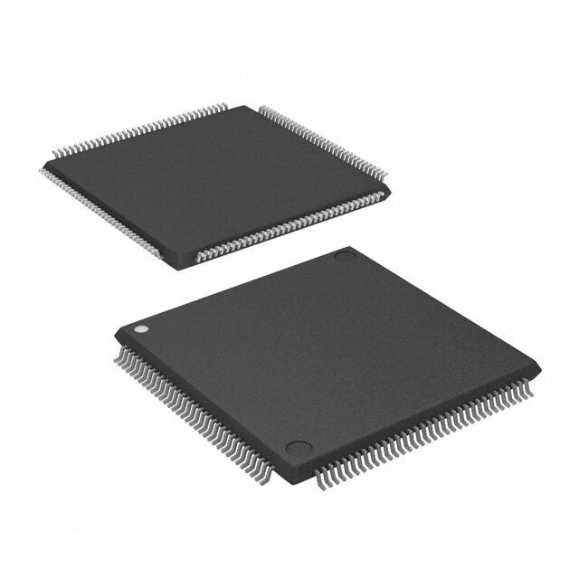
Available in 144-pin Thin Quad Flat Pack (TQFP) and 160-pin
Plastic Ball Grid Array (PBGA) packages
Green package options available
FUNCTIONAL BLOCK DIAGRAM
One of Four Identical Channels
LOS
Detector
RTIPn
Slicer
RRINGn
Analog
Loopback
Peak
Detector
TTIPn
CLK&Data
Recovery
(DPLL)
B8ZS/
HDB3/AMI
Decoder
Jitter
Attenuator
Digital
Loopback
Line
Driver
TRINGn
LOSn
Remote
Loopback
IBLC
Detector
AIS
Detector
B8ZS/
HDB3/AMI
Encoder
Jitter
Attenuator
Waveform
Shaper
RCLKn
RDn/RDPn
CVn/RDNn
TCLKn
TDn/TDPn
BPVIn/TDNn
Transmit
All Ones
JTAG TAP
VDDIO
VDDT
VDDD
VDDA
TRST
TCK
TMS
TDI
TDO
Control Interface
OE
CLKE
MODE[2:0]
CS/JAS
TS2/SCLK/ALE/AS
TS1/RD/R/W
TS0/SDI/WR/DS
SDO/RDY/ACK
INT
LP[3:0]/D[7:0]/AD[7:0]
MC[3:0]/A[4:0]
Register
File
Clock
Generator
MCLK
G.772
Monitor
Figure-1 Block Diagram
IDT and the IDT logo are trademarks of Integrated Device Technology, Inc.
1
2005 Integrated Device Technology, Inc.
September 22, 2005
DSC-6531/-
�IDT82V2044
QUAD T1/E1 SHORT HAUL LINE INTERFACE UNIT
DESCRIPTION
The IDT82V2044 offers hardware control mode and software control
mode. Software control mode works with either serial host interface or
parallel host interface. The latter works via an Intel/Motorola compatible
8-bit parallel interface for both multiplexed or non-multiplexed applications. Hardware control mode uses multiplexed pins to select different
operation modes when the host interface is not available to the device.
The IDT82V2044 is a single chip, 4-channel T1/E1 short haul PCM
transceiver with a reference clock of 1.544 MHz (T1) or 2.048 MHz (E1).
The IDT82V2044 contains 4 transmitters and 4 receivers.
All the receivers and transmitters can be programmed to work either
in Single Rail mode or Dual Rail mode. B8ZS/HDB3 or AMI encoder/
decoder is selectable in Single Rail mode. Pre-encoded transmit data in
NRZ format can be accepted when the device is configured in Dual Rail
mode. The receivers perform clock and data recovery by using integrated digital phase-locked loop. As an option, the raw sliced data (no
retiming) can be output on the receive data pins. Transmit equalization is
implemented with low-impedance output drivers that provide shaped
waveforms to the transformer, guaranteeing template conformance.
The IDT82V2044 also provides loopback and JTAG boundary scan
testing functions. Using the integrated monitoring function, the
IDT82V2044 can be configured as a 4-channel transceiver with nonintrusive protected monitoring points.
The IDT82V2044 can be used for SDH/SONET multiplexers, central
office or PBX, digital access cross connects, digital radio base stations,
remote wireless modules and microwave transmission systems.
A jitter attenuator is integrated in the IDT82V2044 and can be
switched into either the transmit path or the receive path for all channels.
The jitter attenuation performance meets ETSI CTR12/13, ITU G.736,
G.742, G.823, and AT&T Pub 62411 specifications.
IDT82V2044
(Top View)
1
2
3
4
5
6
7
8
9
10
11
12
13
14
15
16
17
18
19
20
21
22
23
24
25
26
27
28
29
30
31
32
33
34
35
36
109
110
111
112
113
114
115
116
117
118
119
120
121
122
123
124
125
126
127
128
129
130
131
132
133
134
135
136
137
138
139
140
141
142
143
144
72
71
70
69
68
67
66
65
64
63
62
61
60
59
58
57
56
55
54
53
52
51
50
49
48
47
46
45
44
43
42
41
40
39
38
37
BPVI3/TDN3
RCLK3
RD3/RDP3
CV3/RDN3
LOS3
RTIP3
RRING3
VDDT
TTIP3
TRING3
GNDT
RRING2
RTIP2
GNDT
TRING2
TTIP2
VDDT
RTIP1
RRING1
VDDT
TTIP1
TRING1
GNDT
RRING0
RTIP0
GNDT
TRING0
TTIP0
VDDT
MODE1
LOS0
CV0/RDN0
RD0/RDP0
RCLK0
BPVI0/TDN0
TD0/TDP0
GNDIO
GNDIO
DNC
DNC
DNC
DNC
GNDIO
GNDIO
GNDIO
MCLK
MODE2
A4
MC3/A3
MC2/A2
MC1/A1
MC0/A0
VDDIO
GNDIO
VDDD
GNDD
LP0/D0/AD0
LP1/D1/AD1
LP2/D2/AD2
LP3/D3/AD3
D4/AD4
D5/AD5
D6/AD6
D7/AD7
TCLK1
TD1/TDP1
BPVI1/TDN1
RCLK1
RD1/RDP1
CV1/RDN1
LOS1
TCLK0
GNDIO
DNC
DNC
DNC
DNC
OE
CLKE
VDDT
DNC
DNC
GNDT
DNC
DNC
GNDT
DNC
DNC
VDDT
DNC
DNC
VDDT
DNC
DNC
GNDT
DNC
DNC
GNDT
DNC
DNC
VDDT
DNC
DNC
DNC
DNC
DNC
DNC
GNDIO
108
107
106
105
104
103
102
101
100
99
98
97
96
95
94
93
92
91
90
89
88
87
86
85
84
83
82
81
80
79
78
77
76
75
74
73
GNDIO
GNDIO
DNC
DNC
DNC
DNC
GNDIO
GNDIO
GNDIO
TDI
TDO
TCK
TMS
TRST
IC
IC
VDDIO
GNDIO
VDDA
GNDA
MODE0/CODE
CS/JAS
TS2/SCLK/ALE/AS
TS1/RD/R/W
TS0/SDI/WR/DS
SDO/RDY/ACK
INT
TCLK2
TD2/TDP2
BPVI2/TDN2
RCLK2
RD2/RDP2
CV2/RDN2
LOS2
TCLK3
TD3/TDP3
PIN CONFIGURATIONS
Figure-2 TQFP144 Package Pin Assignment
Description
2
September 22, 2005
�IDT82V2044
QUAD T1/E1 SHORT HAUL LINE INTERFACE UNIT
A
B
C
D
E
F
G
H
J
K
L
M
N
P
1
DNC
GNDI
O
DNC
GNDI
O
MCLK
MC
1
D6
D7
TCLK
1
RCLK
1
TCLK
0
RCLK
0
1
2
DNC
GNDI
O
DNC
GNDI
O
MODE
2
MC
2
D0
D2
D5
MODE
1
TDP
1
RDP
1
TDP
0
RDP
0
2
3
DNC
GNDI
O
DNC
GNDI
O
DNC
MC
3
MC
0
D1
D4
LOS
1
TDN
1
RDN
1
TDN
0
RDN
0
3
4
VDDT
VDDT
VDDT
VDDT
DNC
A4
D3
LOS
0
VDDT
VDDT
VDDT
VDDT
4
5
DNC
DNC
DNC
DNC
TTIP
1
TRING
1
TTIP
0
TRING
0
5
6
GNDT GNDT GNDT GNDT
GNDT GNDT GNDT GNDT
6
7
DNC
DNC
DNC
DNC
RRING
1
RTIP
1
RRING
0
RTIP
0
7
8
DNC
DNC
DNC
DNC
RRING
2
RTIP
2
RRING
3
RTIP
3
8
9
GNDT GNDT GNDT GNDT
GNDT GNDT GNDT GNDT
9
10
DNC
DNC
DNC
DNC
TTIP
2
TRING
2
TTIP
3
TRING
3
10
11
VDDT
VDDT
VDDT
VDDT
DNC
TMS
GNDIO GNDA
CS
LOS
3
VDDT
VDDT
VDDT
VDDT
11
12
DNC
GNDI
O
DNC
GNDI
O
DNC
TDI
TRST
MODE
0
TS
2
LOS
2
TDN
2
RDN
2
TDN
3
RDN
3
12
13
DNC
GNDI
O
DNC
GNDI
O
CLKE
TDO
IC
IC
TS
1
INT
TDP
2
RDP
2
TDP
3
RDP
3
13
14
DNC
GNDI
O
DNC
GNDI
O
OE
TCK
TS
0
SDO
TCLK
2
RCLK
2
TCLK
3
RCLK
3
14
A
B
C
D
E
F
J
K
L
M
N
P
VDDIO VDDD
GNDIO GNDD
IDT82V2044
(Bottom View)
VDDIO VDDA
G
H
Figure-3 PBGA160 Package Pin Assignment
Pin Configurations
3
September 22, 2005
�IDT82V2044
1
QUAD T1/E1 SHORT HAUL LINE INTERFACE UNIT
PIN DESCRIPTION
Table-1 Pin Description
Name
Type
Pin No.
TQFP144
Description
PBGA160
Transmit and Receive Line Interface
TTIP0
TTIP1
TTIP2
TTIP3
TRING0
TRING1
TRING2
TRING3
RTIP0
RTIP1
RTIP2
RTIP3
RRING0
RRING1
RRING2
RRING3
Analog
Output
Analog
Input
45
52
57
64
N5
L5
L10
N10
46
51
58
63
P5
M5
M10
P10
48
55
60
67
P7
M7
M8
P8
49
54
61
66
N7
L7
L8
N8
TTIPn/TRINGn: Transmit Bipolar Tip/Ring for Channel 0~3
These pins are the differential line driver outputs. They will be in high-Z state if pin OE is low or the corresponding pin TCLKn is low (pin OE is global control, while pin TCLKn is per-channel control). In host
mode, each pin can be in high-Z by programming a ‘1’ to the corresponding bit in register OE(1).
RTIPn/RRINGn: Receive Bipolar Tip/Ring for Channel 0~3
These pins are the differential line receiver inputs.
Transmit and Receive Digital Data Interface
TDn: Transmit Data for Channel 0~3
When the device is in Single Rail mode, the NRZ data to be transmitted is input on this pin. Data on TDn is
sampled into the device on the falling edges of TCLKn, and encoded by AMI or B8ZS/HDB3 line code
rules before being transmitted to the line.
TD0/TDP0
TD1/TDP1
TD2/TDP2
TD3/TDP3
37
30
80
73
N2
L2
L13
N13
38
31
79
72
N3
L3
L12
N12
I
BPVI0/TDN0
BPVI1/TDN1
BPVI2/TDN2
BPVI3/TDN3
BPVIn: Bipolar Violation Insertion for Channel 0~3
Bipolar violation insertion is available in Single Rail mode 2 (see Table-2 on page 13 and Table-3 on page
14) with AMI enabled. A low-to-high transition on this pin will make the next logic one to be transmitted on
TDn the same polarity as the previous pulse, and violate the AMI rule. This is for testing.
TDPn/TDNn: Positive/Negative Transmit Data for Channel 0~3
When the device is in Dual Rail Mode, the NRZ data to be transmitted for positive/negative pulse is input
on this pin. Data on TDPn/TDNn are sampled on the falling edges of TCLKn. The line code in dual rail
mode is as the follow:
TDPn
0
0
1
1
TDNn
0
1
0
1
Output Pulse
Space
Negative Pulse
Positive Pulse
Space
Pulling pin TDNn high for more than 16 consecutive TCLK clock cycles will configure the corresponding
channel into Single Rail mode 1 (see Table-2 on page 13 and Table-3 on page 14).
1. Register name is indicated by bold capital letter. For example, OE indicates Output Enable Register.
Pin Description
4
September 22, 2005
�IDT82V2044
QUAD T1/E1 SHORT HAUL LINE INTERFACE UNIT
Table-1 Pin Description (Continued)
Name
Type
Pin No.
TQFP144
Description
PBGA160
TCLKn: Transmit Clock for Channel 0~3
The clock of 1.544 MHz (for T1 mode) or 2.048 MHz (for E1 mode) for transmit is input on this pin. The
transmit data at TDn/TDPn or TDNn is sampled into the device on the falling edges of TCLKn.
Pulling TCLKn high for more than 16 MCLK cycles, the corresponding transmitter is set in Transmit All
Ones (TAOS) state (when MCLK is clocked). In TAOS state, the TAOS generator adopts MCLK as the
clock reference.
If TCLKn is low, the corresponding transmit channel is set into power down state, while driver output ports
become high-Z.
Different combinations of TCLKn and MCLK result in different transmit mode. It is summarized as the follows:
TCLK0
TCLK1
TCLK2
TCLK3
I
36
29
81
74
N1
L1
L14
N14
MCLK
Clocked
Clocked
Clocked
High/Low
High/Low
TCLKn
Clocked
Transmit Mode
Normal operation
Transmit All Ones (TAOS) signals to the line side in the corresponding
High (≥ 16 MCLK)
transmit channel.
Low (≥ 64 MCLK) The corresponding transmit channel is set into power down state.
TCLKn is clocked Normal operation
Transmit All Ones (TAOS) signals to the line side
TCLKn is high
in the corresponding transmit channel.
(≥ 16 TCLK1)
Corresponding transmit channel is set into power
TCLKn is low
TCLK1 is clocked
down state.
(≥ 64 TCLK1)
The receive path is not affected by the status of TCLK1. When MCLK
is high, all receive paths just slice the incoming data stream. When
MCLK is low, all the receive paths are powered down.
TCLK1 is unavailAll four transmitters (TTIPn & TRINGn) will be in high-Z.
able.
RDn: Receive Data for Channel 0~3
In Single Rail mode, the received NRZ data is output on this pin. The data is decoded by AMI or B8ZS/
HDB3 line code rule.
RD0/RDP0
RD1/RDP1
RD2/RDP2
RD3/RDP3
CV0/RDN0
CV1/RDN1
CV2/RDN2
CV3/RDN3
O
High-Z
Pin Description
40
33
77
70
P2
M2
M13
P13
41
34
76
69
P3
M3
M12
P12
CVn: Code Violation for Channel 0~3
In Single Rail mode, the bipolar violation, code violation and excessive zeros will be reported by driving pin
CVn high for a full clock cycle. However, only bipolar violation is indicated when AMI decoder is selected.
RDPn/RDNn: Positive/Negative Receive Data for Channel 0~3
In Dual Rail Mode with clock recovery, these pins output the NRZ data. A high signal on RDPn indicates
the receipt of a positive pulse on RTIPn/RRINGn while a high signal on RDNn indicates the receipt of a
negative pulse on RTIPn/RRINGn.
The output data at RDn or RDPn/RDNn are clocked out on the falling edges of RCLK when the CLKE input
is low, or are clocked out on the rising edges of RCLK when CLKE is high.
In Dual Rail Mode without clock recovery, these pins output the raw RZ sliced data. In this data recovery
mode, the active polarity of RDPn/RDNn is determined by pin CLKE. When pin CLKE is low, RDPn/RDNn
is active low. When pin CLKE is high, RDPn/RDNn is active high.
In hardware mode, RDn or RDPn/RDNn will remain active during LOS. In host mode, these pins will either
remain active or insert alarm indication signal (AIS) into the receive path, determined by bit AISE in register GCF.
RDn or RDPn/RDNn is set into high-Z when the corresponding receiver is powered down.
5
September 22, 2005
�IDT82V2044
QUAD T1/E1 SHORT HAUL LINE INTERFACE UNIT
Table-1 Pin Description (Continued)
Name
RCLK0
RCLK1
RCLK2
RCLK3
Type
O
High-Z
MCLK
LOS0
LOS1
LOS2
LOS3
Pin No.
TQFP144
39
32
78
71
Description
PBGA160
P1
M1
M14
P14
RCLKn: Receive Clock for Channel 0~3
In clock recovery mode, this pin outputs the recovered clock from signal received on RTIPn/RRINGn. The
received data are clocked out of the device on the rising edges of RCLKn if pin CLKE is high, or on falling
edges of RCLKn if pin CLKE is low.
In data recovery mode, RCLKn is the output of an internal exclusive OR (XOR) which is connected with
RDPn and RDNn. The clock is recovered from the signal on RCLKn.
If Receiver n is powered down, the corresponding RCLKn is in high-Z.
I
10
E1
MCLK: Master Clock
This is an independent, free running reference clock. A clock of 1.544 MHz (for T1 mode) or 2.048 MHz
(for E1 mode) is supplied to this pin as the clock reference of the device for normal operation.
In receive path, when MCLK is high, the device slices the incoming bipolar line signal into RZ pulse (Data
Recovery mode). When MCLK is low, all the receivers are powered down, and the output pins RCLKn,
RDPn and RDNn are switched to high-Z.
In transmit path, the operation mode is decided by the combination of MCLK and TCLKn (see TCLKn pin
description for details).
NOTE: Wait state generation via RDY/ACK is not available if MCLK is not provided.
O
42
35
75
68
K4
K3
K12
K11
LOSn: Loss of Signal Output for Channel 0~3
A high level on this pin indicates the loss of signal when there is no transition over a specified period of
time or no enough ones density in the received signal. The transition will return to low automatically when
there is enough transitions over a specified period of time with a certain ones density in the received signal. The LOS assertion and desertion criteria are described in 2.4.4 Loss of Signal (LOS) Detection.
Hardware/Host Control Interface
MODE2: Control Mode Select 2
The signal on this pin determines which control mode is selected to control the device:
MODE2
Low
VDDIO/2
High
I
MODE2
(Pulled to
VDDIO/2)
11
E2
Control Interface
Hardware Mode
Serial Host Interface
Parallel Host Interface
Hardware control pins include MODE[2:0], TS[2:0], LP[3:0], CODE, CLKE, JAS and OE.
Serial host Interface pins include CS, SCLK, SDI, SDO and INT.
Parallel host Interface pins include CS, A[4:0], D[7:0], WR/DS, RD/R/W, ALE/AS, INT and RDY/ACK. The
device supports multiple parallel host interface as follows (refer to MODE1 and MODE0 pin descriptions
below for details):
MODE[2:0]
100
101
110
111
MODE1
Pin Description
I
43
K2
Host Interface
Non-multiplexed Motorola Interface
Non-multiplexed Intel Interface
Multiplexed Motorola Interface
Multiplexed Intel Interface
MODE1: Control Mode Select 1
In parallel host mode, the parallel interface operates with separate address bus and data bus when this pin
is low, and operates with multiplexed address and data bus when this pin is high.
In serial host mode or hardware mode, this pin should be grounded.
6
September 22, 2005
�IDT82V2044
QUAD T1/E1 SHORT HAUL LINE INTERFACE UNIT
Table-1 Pin Description (Continued)
Name
Type
Pin No.
TQFP144
Description
PBGA160
MODE0: Control Mode Select 0
In parallel host mode, the parallel host interface is configured for Motorola compatible hosts when this pin
is low, or for Intel compatible hosts when this pin is high.
MODE0/CODE
I
88
H12
CODE: Line Code Rule Select
In hardware control mode, the B8ZS (for T1 mode)/HDB3 (for E1 mode) encoder/decoder is enabled when
this pin is low, and AMI encoder/decoder is enabled when this pin is high. The selections affect all the
channels.
In serial host mode, this pin should be grounded.
CS: Chip Select (Active Low)
In host mode, this pin is asserted low by the host to enable host interface. A high to low transition must
occur on this pin for each read/write operation and the level must not return to high until the operation is
over.
I
CS/JAS
(Pulled to
VDDIO/2)
87
J11
JAS: Jitter Attenuator Select
In hardware control mode, this pin globally determines the Jitter Attenuator position:
JAS
Low
VDDIO/2
High
Jitter Attenuator (JA) Configuration
JA in transmit path
JA not used
JA in receive path
TS2: Template Select 2
In hardware control mode, the signal on this pin is the most significant bit for the transmit template select.
Refer to 2.5.1 Waveform Shaper for details.
TS2/SCLK/
ALE/AS
I
86
J12
SCLK: Shift Clock
In serial host mode, the signal on this pin is the shift clock for the serial interface. Data on pin SDO is
clocked out on falling edges of SCLK if pin CLKE is high, or on rising edges of SCLK if pin CLKE is low.
Data on pin SDI is always sampled on rising edges of SCLK.
ALE: Address Latch Enable
In parallel Intel multiplexed host mode, the address on AD[4:0] is sampled into the device on the falling
edges of ALE (signals on AD[7:5] are ignored). In non-multiplexed host mode, ALE should be pulled high.
AS: Address Strobe (Active Low)
In parallel Motorola multiplexed host mode, the address on AD[4:0] is latched into the device on the falling
edges of AS (signals on AD[7:5] are ignored). In non-multiplexed host mode, AS should be pulled high.
TS1: Template Select 1
In hardware control mode, the signal on this pin is the second most significant bit for the transmit template
select. Refer to 2.5.1 Waveform Shaper for details.
TS1/RD/R/W
I
85
J13
RD: Read Strobe (Active Low)
In parallel Intel multiplexed or non-multiplexed host mode, this pin is active low for read operation.
R/W: Read/Write Select
In parallel Motorola multiplexed or non-multiplexed host mode, the pin is active low for write operation and
high for read operation.
Pin Description
7
September 22, 2005
�IDT82V2044
QUAD T1/E1 SHORT HAUL LINE INTERFACE UNIT
Table-1 Pin Description (Continued)
Name
Type
Pin No.
TQFP144
Description
PBGA160
TS0: Template Select 0
In hardware control mode, the signal on this pin is the least significant bit for the transmit template select.
Refer to 2.5.1 Waveform Shaper for details.
SDI: Serial Data Input
In serial host mode, this pin input the data to the serial interface. Data on this pin is sampled on the rising
edges of SCLK.
TS0/SDI/WR/
DS
I
84
J14
WR: Write Strobe (Active Low)
In parallel Intel host mode, this pin is active low during write operation. The data on D[7:0] (in non-multiplexed mode) or AD[7:0] (in multiplexed mode) is sampled into the device on the rising edges of WR.
DS: Data Strobe (Active Low)
In parallel Motorola host mode, this pin is active low. During a write operation (R/W = 0), the data on D[7:0]
(in non-multiplexed mode) or AD[7:0] (in multiplexed mode) is sampled into the device on the rising edges
of DS. During a read operation (R/W = 1), the data is driven to D[7:0] (in non-multiplexed mode) or AD[7:0]
(in multiplexed mode) by the device on the rising edges of DS.
In parallel Motorola non-multiplexed host mode, the address information on the 5 bits of address bus
A[4:0] are latched into the device on the falling edges of DS.
SDO: Serial Data Output
In serial host mode, the data is output on this pin. In serial write operation, SDO is always in high-Z. In
serial read operation, SDO is in high-Z only when SDI is in address/command byte. Data on pin SDO is
clocked out of the device on the falling edges of SCLK if pin CLKE is high, or on the rising edges of SCLK
if pin CLKE is low.
SDO/RDY/ACK
O
83
K14
RDY: Ready Output
In parallel Intel host mode, the high level of this pin reports to the host that bus cycle can be completed,
while low reports the host must insert wait states.
ACK: Acknowledge Output (Active Low)
In parallel Motorola host mode, the low level of this pin indicates that valid information on the data bus is
ready for a read operation or acknowledges the acceptance of the written data during a write operation.
INT
O
Open
Drain
82
K13
INT: Interrupt (Active Low)
This is the open drain, active low interrupt output. Four sources may cause the interrupt. Refer to 2.20
Interrupt Handling for details.
LPn: Loopback Select 3~0
In hardware control mode, pin LPn configures the corresponding channel in different loopback mode, as
follows:
D7/AD7
D6/AD6
D5/AD5
D4/AD4
LP3/D3/AD3
LP2/D2/AD2
LP1/D1/AD1
LP0/D0/AD0
I/O
High-Z
28
27
26
25
24
23
22
21
K1
J1
J2
J3
J4
H2
H3
G2
LPn
Low
VDDIO/2
High
Loopback Configuration
Remote Loopback
No loopback
Analog Loopback
Refer to 2.13 Loopback Mode for details.
In hardware control mode, D4 to D7 should be tied to VDDIO/2.
Dn: Data Bus 7~0
In non-multiplexed host mode, these pins are the bi-directional data bus.
ADn: Address/Data Bus 7~0
In multiplexed host mode, these pins are the multiplexed bi-directional address/data bus.
In serial host mode, these pins should be grounded.
Pin Description
8
September 22, 2005
�IDT82V2044
QUAD T1/E1 SHORT HAUL LINE INTERFACE UNIT
Table-1 Pin Description (Continued)
Name
Type
A4
MC3/A3
MC2/A2
MC1/A1
MC0/A0
I
Pin No.
TQFP144
12
13
14
15
16
Description
PBGA160
F4
F3
F2
F1
G3
MCn: Performance Monitor Configuration 3~0
In hardware control mode, A4 must be connected to GND. MC[3:0] are used to select one transmitter or
receiver of channel 1 to 4 for non-intrusive monitoring. Channel 0 is used as the monitoring channel. If a
transmitter is monitored, signals on the corresponding pins TTIPn and TRINGn are internally transmitted
to RTIP0 and RRING0. If a receiver is monitored, signals on the corresponding pins RTIPn and RRINGn
are internally transmitted to RTIP0 and RRING0. The clock and data recovery circuit in Receiver 0 can
then output the monitored clock to pin RCLK0 as well as the monitored data to RDP0 and RDN0 pins. The
signals monitored by channel 0 can be routed to TTIP0/TRING0 by activating Remote Loopback in this
channel.
Performance Monitor Configuration determined by MC[3:0] is shown below. Note that if MC[2:0] = 000, the
device is in normal operation of all the channels.
MC[3:0]
Monitoring Configuration
0000
Normal operation without monitoring
0001
Monitor Receiver 1
0010
Monitor Receiver 2
0011
Monitor Receiver 3
0100
0101
Reserved
0110
0111
1000
Normal operation without monitoring
1001
Monitor Transmitter 1
1010
Monitor Transmitter 2
1011
Monitor Transmitter 3
1100
1101
Reserved
1110
1111
An: Address Bus 4~0
When pin MODE1 is low, the parallel host interface operates with separate address and data bus. In this
mode, the signal on this pin is the address bus of the host interface.
OE
I
CLKE
I
114
115
E14
OE: Output Driver Enable
Pulling this pin low can drive all driver output into high-Z for redundancy application without external
mechanical relays. In this condition, all other internal circuits remain active.
E13
CLKE: Clock Edge Select
The signal on this pin determines the active edge of RCLKn and SCLK in clock recovery mode, or determines the active level of RDPn and RDNn in the data recovery mode. See 2.3 Clock Edges on page 14 for
details.
JTAG Signals
I
TRST
95
G12
TRST: JTAG Test Port Reset (Active Low)
This is the active low asynchronous reset to the JTAG Test Port. This pin has an internal pull-up resistor
and can be left disconnected.
96
F11
TMS: JTAG Test Mode Select
The signal on this pin controls the JTAG test performance and is clocked into the device on the rising
edges of TCK. This pin has an internal pull-up resistor and it can be left disconnected.
F14
TCK: JTAG Test Clock
This pin input the clock of the JTAG Test. The data on TDI and TMS are clocked into the device on the rising edges of TCK, while the data on TDO is clocked out of the device on the falling edges of TCK. This pin
should be connected to GNDIO or VDDIO pin when unused.
Pull-up
I
TMS
Pull-up
TCK
Pin Description
I
97
9
September 22, 2005
�IDT82V2044
QUAD T1/E1 SHORT HAUL LINE INTERFACE UNIT
Table-1 Pin Description (Continued)
Name
Type
Pin No.
TQFP144
98
F13
TDO: JTAG Test Data Output
This pin output the serial data of the JTAG Test. The data on TDO is clocked out of the device on the falling edges of TCK. TDO is a high-Z output signal. It is active only when scanning of data is out. This pin
should be left float when unused.
99
F12
TDI: JTAG Test Data Input
This pin input the serial data of the JTAG Test. The data on TDI is clocked into the device on the rising
edges of TCK. This pin has an internal pull-up resistor and it can be left disconnected.
O
TDO
High-Z
I
TDI
Description
PBGA160
Pull-up
Power Supplies and Grounds
-
17
92
G1
G14
3.3 V I/O Power Supply
-
1
2
7
8
9
18
91
100
101
102
107
108
109
144
B1
B2
B3
B12
B13
B14
D1
D2
D3
D12
D13
D14
G4
G11
I/O GND
-
44
53
56
65
116
125
128
137
A4, A11
B4, B11
C4, C11
D4, D11
L4, L11
M4, M11
N4, N11
P4, P11
3.3 V/5 V Power Supply for Transmitter Driver
All VDDT pins must be connected to 3.3 V or all VDDT must be connected to 5 V. It is not allowed to leave
any of the VDDT pins open (not-connected) even if the channel is not used.
For T1 applications, only 5 V VDDT is supported.
GNDT
-
47
50
59
62
119
122
131
134
A6, A9
B6, B9
C6, C9
D6, D9
L6, L9
M6, M9
N6, N9
P6, P9
Analog GND for Transmitter Driver
VDDD
-
19
H1
3.3 V Digital Core Power Supply
VDDA
-
90
H14
3.3 V Analog Core Power Supply
GNDD
-
20
H4
Digital Core GND
GNDA
-
89
H11
Analog Core GND
VDDIO
GNDIO
VDDT
Pin Description
10
September 22, 2005
�IDT82V2044
QUAD T1/E1 SHORT HAUL LINE INTERFACE UNIT
Table-1 Pin Description (Continued)
Name
Type
Pin No.
TQFP144
Description
PBGA160
Others
IC
DNC
Pin Description
-
93
94
G13
H13
IC: Internal Connection
Internal use. Leave it open for normal operation.
-
3
4
5
6
103
104
105
106
110
111
112
113
117
118
120
121
123
124
126
127
129
130
132
133
135
136
138
139
140
141
142
143
A1
A2
A3
A5
A7
A8
A10
A12
A13
A14
B5
B7
B8
B10
C1
C2
C3
C5
C7
C8
C10
C12
C13
C14
D5
D7
D8
D10
E3
E4
E11
E12
DNC: Do Not Connect
11
September 22, 2005
�IDT82V2044
QUAD T1/E1 SHORT HAUL LINE INTERFACE UNIT
2
FUNCTIONAL DESCRIPTION
2.1
OVERVIEW
The Dual Rail interface consists of TDPn1, TDNn, TCLKn, RDPn,
RDNn and RCLKn. Data transmitted from TDPn and TDNn appears on
TTIPn and TRINGn at the line interface; data received from the RTIPn
and RRINGn at the line interface are transferred to RDPn and RDNn
while the recovered clock extracting from the received data stream
outputs on RCLKn. In Dual Rail operation, the clock/data recovery mode
is selectable. Dual Rail interface with clock recovery shown in Figure-4
is a default configuration mode. Dual Rail interface with data recovery is
shown in Figure-5. Pin RDPn and RDNn, in this condition, are raw RZ
slice output and internally connected to an EXOR which is fed to the
RCLKn output for external clock recovery applications.
The IDT82V2044 is a fully integrated quad short-haul line interface
unit, which contains four transmit and receive channels for use in either
T1 or E1 applications. The receiver performs clock and data recovery.
As an option, the raw sliced data (no retiming) can be output to the
system. Transmit equalization is implemented with low-impedance
output drivers that provide shaped waveforms to the transformer, guaranteeing template conformance. A selectable jitter attenuator may be
placed in the receive path or the transmit path. Moreover, multiple
testing functions, such as error detection, loopback and JTAG boundary
scan are also provided. The device is optimized for flexible software
control through a serial or parallel host mode interface. Hardware control
is also available. Figure-1 on page 1 shows one of the four identical
channels operation.
2.2
In Single Rail mode, data transmitted from TDn appears on TTIPn
and TRINGn at the line interface. Data received from the RTIPn and
RRINGn at the line interface appears on RDn while the recovered clock
extracting from the received data stream outputs on RCLKn. When the
device is in single rail interface, the selectable AMI or B8ZS/HDB3 line
encoder/decoder is available and any code violation in the received data
will be indicated at the CVn pin. The Single Rail mode has 2 sub-modes:
Single Rail Mode 1 and Single Rail Mode 2. Single Rail Mode 1, whose
interface is composed of TDn, TCLKn, RDn, CVn and RCLKn, is realized by pulling pin TDNn high for more than 16 consecutive TCLK
cycles. Single Rail Mode 2, whose interface is composed of TDn,
TCLKn, RDn, CVn, RCLKn and BPVIn, is realized by setting bit CRS in
register e-CRS2 and bit SING in register e-SING. The difference
between them is that, in the latter mode bipolar violation can be inserted
via pin BPVIn if AMI line code is selected.
T1/E1 MODE SELECTION
T1/E1 mode selection configures the device globally. In Hardware
Mode, the template selection pins TS[2:0], determine whether the operation mode is T1 or E1 (see Table-9 on page 18). In Software Mode, the
register TS determines whether the operation mode is T1 or E1.
2.2.1 SYSTEM INTERFACE
The system interface of each channel can be configured to operate
in different modes:
1. Single rail interface with clock recovery.
2. Dual rail interface with clock recovery.
3. Dual rail interface with data recovery (that is, with raw data
slicing only and without clock recovery).
The configuration of the Hardware Mode System Interface is summarized in Table-2. The configuration of the Host (Software) Mode System
Interface is summarized Table-3.
1. The footprint ‘n’ (n = 0 - 3) indicates one of the four channels.
Each signal pin on system side has multiple functions depending on
which operation mode the device is in.
2. The first letter ‘e-’ indicates expanded register.
LOS
Detector
RTIPn
Slicer
RRINGn
One of Four Identical Channels
LOSn
CLK&Data
Recovery
(DPLL)
Jitter
Attenuator
B8ZS/
HDB3/AMI
Decoder
RCLKn
RDPn
RDNn
Waveform
Shaper
Jitter
Attenuator
B8ZS/
HDB3/AMI
Encoder
TCLKn
TDPn
TDNn
Peak
Detector
TTIPn
TRINGn
Line
Driver
Transmit
All Ones
Note: The grey blocks are bypassed and the dotted blocks are selectable.
Figure-4 Dual Rail Interface with Clock Recovery
Functional Description
12
September 22, 2005
�IDT82V2044
QUAD T1/E1 SHORT HAUL LINE INTERFACE UNIT
One of Four Identical Channels
LOS
Detector
RTIPn
Slicer
RRINGn
LOSn
CLK&Data
Recovery
(DPLL)
Jitter
Attenuator
B8ZS/
HDB3/AMI
Decoder
Waveform
Shaper
Jitter
Attenuator
B8ZS/
HDB3/AMI
Encoder
RCLKn
(RDP RDN)
RDPn
RDNn
Peak
Detector
TTIPn
Line
Driver
TRINGn
TCLKn
TDPn
TDNn
Transmit
All Ones
Note: The grey blocks are bypassed and the dotted blocks are selectable.
Figure-5 Dual Rail Interface with Data Recovery
LOS
Detector
RTIPn
Slicer
RRINGn
One of Four Identical Channels
LOSn
CLK&Data
Recovery
(DPLL)
Jitter
Attenuator
B8ZS/
HDB3/AMI
Decoder
Waveform
Shaper
Jitter
Attenuator
B8ZS/
HDB3/AMI
Encoder
RCLKn
RDn
CVn
Peak
Detector
TTIPn
TRINGn
Line
Driver
TCLKn
TDn
BPVIn/TDNn
Transmit
All Ones
Figure-6 Single Rail Mode
Table-2 System Interface Configuration (In Hardware Mode)
Pin MCLK
Pin TDNn
Clocked
High (≥ 16 MCLK)
Interface
Single Rail Mode 1
Clocked
Pulse
Dual Rail mode with Clock Recovery
High
Pulse
Receive just slices the incoming data. Transmit is determined by the status of TCLKn.
Low
Pulse
Receiver n is powered down. Transmit is determined by the status of TCLKn.
Functional Description
13
September 22, 2005
�IDT82V2044
QUAD T1/E1 SHORT HAUL LINE INTERFACE UNIT
Table-3 System Interface Configuration (In Host Mode)
Pin MCLK
Pin TDNn
CRSn in e-CRS
SINGn in e-SING
Interface
Clocked
Clocked
Clocked
Clocked
High
Low
High
Pulse
Pulse
Pulse
Pulse
Pulse
0
0
0
1
-
0
1
0
0
-
Single Rail Mode 1
Single Rail Mode 2
Dual Rail mode with Clock Recovery
Dual Rail mode with Data Recovery
Receive just slices the incoming data. Transmit is determined by the status of TCLKn.
Receiver n is powered down. Transmit is determined by the status of TCLKn.
Table-4 Active Clock Edge and Active Level
Pin RDn/RDPn and CVn/RDNn
Clock Recovery
Slicer Output
Pin CLKE
2.3
High
RCLKn
Active High
Active High
SCLK
Active High
Low
RCLKn
Active High
Active Low
SCLK
Active High
CLOCK EDGES
data recovery mode, the slicer output is sent to Clock and Data
Recovery circuit for abstracting retimed data and optional decoding. The
slicer circuit has a built-in peak detector from which the slicing threshold
is derived. The slicing threshold is default to 50% (typical) of the peak
value.
The active edge of RCLKn and SCLK are selectable. If pin CLKE is
high, the active edge of RCLKn is the rising edge, as for SCLK, that is
falling edge. On the contrary, if CLKE is low, the active edge of RCLK is
the falling edge and that of SCLK is rising edge. Pins RDn/RDPn, CVn/
RDNn and SDO are always active high, and those output signals are
clocked out on the active edge of RCLKn and SCLK respectively. See
Table-4 Active Clock Edge and Active Level on page 14 for details.
However, in dual rail mode without clock recovery, pin CLKE is used to
set the active level for RDPn/RDNn raw slicing output: High for active
high polarity and low for active low. It should be noted that data on pin
SDI are always active high and are sampled on the rising edges of
SCLK. The data on pin TDn/TDPn or BPVIn/TDNn are also always
active high but is sampled on the falling edges of TCLK, despite the level
on CLKE.
2.4
Pin SDO
Signals with an attenuation of up to 12 dB (from 2.4 V) can be recovered by the receiver. To provide immunity from impulsive noise, the peak
detectors are held above a minimum level of 0.150 V typically, despite
the received signal level.
2.4.2 CLOCK AND DATA RECOVERY
The Clock and Data Recovery is accomplished by Digital Phase
Locked Loop (DPLL). The DPLL is clocked 16 times of the received
clock rate, i.e. 24.704 MHz in T1 mode or 32.768 MHz in E1 mode. The
recovered data and clock from DPLL is then sent to the selectable Jitter
Attenuator or decoder for further processing.
RECEIVER
The clock recovery and data recovery can be selected on a per
channel basis by setting bit CRSn in register e-CRS. When bit CRSn is
defaulted to ‘0’, the corresponding channel operates in data and clock
recovery mode. The recovered clock is output on pin RCLKn and retimed NRZ data are output on pin RDPn/RDNn in Dual Rail mode or on
RDn in single rail mode. When bit CRSn is set to ‘1’, Dual Rail mode with
data recovery is enabled in the corresponding channel and the clock
recovery is bypassed. In this condition, the analog line signal are
converted to RZ digital bit streams on the RDPn/RDNn pins and internally connected to an EXOR which is fed to the RCLKn output for
external clock recovery applications.
In receive path, the line signals couple into RRINGn and RTIPn via a
transformer and are converted into RZ digital pulses by a data slicer.
Adaptation for attenuation is achieved using an integral peak detector
that sets the slicing levels. Clock and data are recovered from the
received RZ digital pulses by a digital phase-locked loop that provides
jitter accommodation. After passing through the selectable jitter attenuator, the recovered data are decoded using B8ZS/HDB3 or AMI line
code rules and clocked out of pin RDn in single rail mode, or presented
on RDPn/RDNn in an undecoded dual rail NRZ format. Loss of signal,
alarm indication signal, line code violation and excessive zeros are
detected. The presence of programmable inband loopback codes are
also detected. These various changes in status may be enabled to
generate interrupts.
If pin MCLK is pulled high, all the receivers will enter the Dual Rail
mode with data recovery. In this case, register e-CRS is ignored.
2.4.3 B8ZS/HDB3/AMI LINE CODE RULE
Selectable B8ZS/HDB3 and AMI line coding/decoding is provided
when the device is configured in Single Rail mode. B8ZS rules for T1
and HDB3 rules for E1 are enabled by setting bit CODE in register GCF
2.4.1 PEAK DETECTOR AND SLICER
The slicer determines the presence and polarity of the received
pulses. In data recovery mode, the raw positive slicer output appears on
RDPn while the negative slicer output appears on RDNn. In clock and
Functional Description
14
September 22, 2005
�IDT82V2044
QUAD T1/E1 SHORT HAUL LINE INTERFACE UNIT
2.4.4 LOSS OF SIGNAL (LOS) DETECTION
The Loss of Signal Detector monitors the amplitude and density of
the received signal on receiver line before the transformer (measured on
port A, B shown in Figure-12). The loss condition is reported by pulling
pin LOSn high. At the same time, LOS alarm registers track LOS condition. When LOS is detected or cleared, an interrupt will generate if not
masked. In host mode, the detection supports the ANSI T1.231 for T1
mode, ITU G.775 and ETSI 300 233 for E1 mode. In hardware mode, it
supports the ITU G.775 and ANSI T1.231.
to ‘0’ or pulling pin CODE low. AMI rule is enabled by setting bit CODE in
register GCF to ‘1’ or pulling pin CODE high. The settings affect all four
channels.
Line code rule selection for each channel, if needed, is available by
setting bit SINGn in register e-SING to ‘1’ (to activate bit CODEn in
register e-CODE) and programming bit CODEn to select line code rules
in the corresponding channel: ‘0’ for B8ZS/HDB3, while ‘1’ for AMI. In
this case, the value in bit CODE in register GCF or pin CODE for global
control is unaffected in the corresponding channel and only affect in
other channels.
Table-6 summarizes the conditions of LOS in clock recovery mode.
In dual rail mode, the decoder/encoder are bypassed. Bit CODE in
register GCF, bit CODEn in register e-CODE and pin CODE are ignored.
During LOS, the RDPn/RDNn output the sliced data when bit AISE in
register GCF is set to ‘0’ or output all ones as AIS (alarm indication
signal) when bit AISE is set to ‘1’. The RCLKn is replaced by MCLK only
if the bit AISE is set.
The configuration of the line code rule is summarized in Table-5.
Table-5 Configuration of the Line Code Rule
Hardware Mode
Line Code Rule
CODE
Low
CODE in GCF
0
0
1
1
0
1
All channels in B8ZS/HDB3
High
All channels in AMI
CODEn in e-CODE
0/1
0
0/1
1
1
0
Host Mode
SINGn in e-SING
0
1
0
1
1
1
Line Code Rule
All channels in B8ZS/HDB3
All channels in AMI
CHn in AMI
CHn in B8ZS/HDB3
Table-6 LOS Condition in Clock Recovery Mode
Standard
ANSI T1.231 for T1
LOS
Detected
Continuous Intervals
LOS
Cleared
Density
Amplitude(1)
Amplitude(1)
1.
G.775 for E1
175
below typical 200 mVp
ETSI 300 233 for E1
32
2048 (1 ms)
below typical 200 mVp
below typical 200 mVp
12.5% (16 marks in a sliding 128-bit 12.5% (4 marks in a sliding 32-bit
period) with no more than 99 contin- period) with no more than 15 conuous zeros
tinuous zeros
12.5% (4 marks in a sliding 32-bit
period) with no more than 15 continuous zeros
exceed typical 250 mVp
exceed typical 250 mVp
exceed typical 250 mVp
Signal on
LOSn
High
Low
LOS levels at device (RTIPn, RRINGn) with all ones signal. For more detail regarding the LOS parameters, please refer to Receiver Characteristics on page 48.
2.4.5 ALARM INDICATION SIGNAL (AIS) DETECTION
Alarm Indication Signal is available only in host mode with clock
recovery, as shown in Table-7.
Table-7 AIS Condition
AIS Detected
AIS Cleared
ITU G.775 for E1
(Register LAC defaulted to ‘0’)
ETSI 300 233 for E1
(Register LAC set to ‘1’)
ANSI T1.231 for T1
Less than 3 zeros contained in each of two
consecutive 512-bit stream are received
3 or more zeros contained in each of two
consecutive 512-bit stream are received
Less than 3 zeros contained in a 512-bit
stream are received
3 or more zeros contained in a 512-bit
stream are received
Less than 9 zeros contained in a 8192-bit stream (a ones
density of 99.9% over a period of 5.3 ms) are received
9 or more zeros contained in a 8192-bit stream are
received
Functional Description
15
September 22, 2005
�IDT82V2044
QUAD T1/E1 SHORT HAUL LINE INTERFACE UNIT
and e-CODV are used to determine whether excessive zeros and code
violation are reported respectively. When the device is configured in AMI
decoding mode, only bipolar violation can be reported.
2.4.6 ERROR DETECTION
The device can detect excessive zeros, bipolar violation and B8ZS/
HDB3 code violation, as shown in Figure-7, Figure-8 and Figure-9. All
the three kinds of errors are reported in both host mode and hardware
mode with B8ZS/HDB3 line code rule used. In host mode, the e-CZER
The error detection is available only in single rail mode in which the
pin CVn/RDNn is used as error report output (CVn pin).
The configuration and report status of error detection are summarized in Table-8.
Table-8 Error Detection
Hardware Mode
Host Mode
Line Code
Pin CVn Reports
Line Code
CODVn in e-CODV CZERn in e-CZER
AMI
Bipolar Violation
AMI
B8ZS/
HDB3
Bipolar Violation +
Code Violation
+ Excessive Zeros
B8ZS/HDB3
0
0
1
1
Pin CVn Reports
0
1
0
1
Bipolar Violation
Bipolar Violation + Code Violation
Bipolar Violation + Code Violation + Excessive Zeros
Bipolar Violation
Bipolar Violation + Excessive Zeros
RCLKn
RTIPn
1
RRINGn
3
5
2
V
4
RDn
1
7
6
2
3
4
5
V
6
CVn
Bipolar Violation
Bipolar Violation detected
Figure-7 AMI Bipolar Violation
Code violation
RCLKn
RTIPn
1
3
5
4 consecutive zeros
RRINGn
RDn
2
4
1
V
2
3
V
6
4
5
6
CVn
Excessive zeros detected
Code violation detected
Figure-8 HDB3 Code Violation & Excessive Zeros
Functional Description
16
September 22, 2005
�IDT82V2044
QUAD T1/E1 SHORT HAUL LINE INTERFACE UNIT
RCLKn
RTIPn
2
4
6
8
8 consecutive zeros
RRINGn
RDn
1
3
5
1
2
7
3
4
9
5
6
7
8
CVn
Excessive zeros detected
Figure-9 B8ZS Excessive Zeros
2.5
TRANSMITTER
1.2
In transmit path, data in NRZ format are clocked into the device on
TDn and encoded by AMI or B8ZS/HDB3 line code rules when single rail
mode is configured or pre-encoded data in NRZ format are input on
TDPn and TDNn when dual rail mode is configured. The data are
sampled into the device on falling edges of TCLKn. Jitter attenuator, if
enabled, is provided with a FIFO through which the data to be transmitted are passing. A low jitter clock is generated by an integral digital
phase-locked loop and is used to read data from the FIFO. The shape of
the pulses are user programmable to ensure that the T1/E1 pulse
template is met after the signal passes through different cable lengths or
types. Bipolar violation, for diagnosis, can be inserted on pin BPVIn if
AMI line code rule is enabled.
1
Normalized Amplitude
0.8
0.6
0.4
0.2
0
-0.2
-0.4
-0.6
0
2.5.1 WAVEFORM SHAPER
T1 pulse template, specified in the DSX-1 Cross-Connect by ANSI
T1.102, is illustrated in Figure-10. The device has built-in transmit waveform templates, corresponding to 5 levels of pre-equalization for cable of
a length from 0 to 655 ft with each increment of 133 ft.
500
750
1000
1250
Time (ns)
Figure-10 DSX-1 Waveform Template
1.20
E1 pulse template, specified in ITU-T G.703, is shown in Figure-11.
The device has built-in transmit waveform templates for cable of 75 Ω or
120 Ω.
1.00
Normalized Amplitude
0.80
Any one of the six built-in waveforms can be chosen in both hardware mode and host mode. In hardware mode, setting pins TS[2:0] can
select the required waveform template for all the transmitters, as shown
in Table-9. In host mode, the waveform template can be configured on a
per-channel basis. Bits TSIA[2:0] in register TSIA are used to select the
channel and bits TS[2:0] in register TS are used to select the required
waveform template.
0.60
0.40
0.20
0.00
The built-in waveform shaper uses an internal high frequency clock
which is 16XMCLK as the clock reference. This function will be
bypassed when MCLK is unavailable.
Functional Description
250
-0.20
-300
-200
-100
0
Time (ns)
100
200
300
Figure-11 CEPT Waveform Template
17
September 22, 2005
�IDT82V2044
QUAD T1/E1 SHORT HAUL LINE INTERFACE UNIT
Table-9 Built-in Waveform Template Selection
TS2
TS1
TS0
Service
Clock Rate
Cable Length
Maximum Cable Loss (dB)(1)
0
0
0
E1
2.048 MHz
120 Ω/75 Ω Cable
-
0
0
0
1
1
1
1
0
1
1
0
0
1
1
1
0
1
0
1
0
1
Reserved
T1
0-133 ft. ABAM
133-266 ft. ABAM
266-399 ft. ABAM
399-533 ft. ABAM
533-655 ft. ABAM
1.544 MHz
1. Maximum cable loss at 772 kHz.
through the jitter attenuator in the corresponding transmit or receive
path. The constant delay feature is crucial for the applications requiring
“hitless” switching.
2.5.2 BIPOLAR VIOLATION INSERTION
When configured in Single Rail Mode 2 with AMI line code enabled,
pin TDNn/BPVIn is used as BPVI input. A low-to-high transition on this
pin inserts a bipolar violation on the next available mark in the transmit
data stream. Sampling occurs on the falling edges of TCLK. But in TAOS
(Transmit All Ones) with Analog Loopback, Remote Loopback and
Inband Loopback, the BPVI is disabled. In TAOS with Digital Loopback,
the BPVI is looped back to the system side, so the data to be transmitted
on TTINGn and TRINGn are all ones with no bipolar violation.
2.6
0.6
1.2
1.8
2.4
3.0
Table-10 Gap Width Limitation
FIFO Length
64 bit
32 bit
Max. Gap Width
56 UI
28 UI
In host mode, bit JABW in GCF determines the jitter attenuator 3 dB
corner frequency (fc) for both T1 and E1. In hardware mode, the fc is
fixed to 2.5 Hz for T1 or 1.7 Hz for E1. Generally, the lower the fc is, the
higher the attenuation. However, lower fc comes at the expense of
increased acquisition time. Therefore, the optimum fc is to optimize both
the attenuation and the acquisition time. In addition, the longer FIFO
length results in an increased throughput delay and also influences the 3
dB corner frequency. Generally, it’s recommended to use the lower
corner frequency and the shortest FIFO length that can still meet jitter
attenuation requirements.
JITTER ATTENUATOR
The jitter attenuator can be selected to work either in transmit path or
in receive path or not used. The selection is accomplished by setting pin
JAS in hardware mode or configuring bits JACF[1:0] in register GCF in
host mode which affects all four channels.
For applications which require line synchronization, the line clock
needed to be extracted for the internal synchronization, the jitter attenuator is set in the receive path. Another use of the jitter attenuator is to
provide clock smoothing in the transmit path for applications such as
synchronous/asynchronous demultiplexing applications. In these applications, TCLK will have an instantaneous frequency that is higher than
the nominal T1/E1 data rate and in order to set the average long-term
TCLK frequency within the transmit line rate specifications, periods of
TCLK are suppressed (gapped).
Table-11 Output Jitter Specification
T1
AT&T Pub 62411
GR-253-CODE
TR-TSY-000009
The jitter attenuator integrates a FIFO which can accommodate a
gapped TCLK. In host mode, the FIFO length can be 32 X 2 or 64 X 2
bits by programming bit JADP in GCF. In hardware mode, it is fixed to 64
X 2 bits. The FIFO length determines the maximum permissible gap
width (see Table-10 Gap Width Limitation). Exceeding these values will
cause FIFO overflow or underflow. The data is 16 or 32 bits’ delay
2.7
E1
ITU-T G.736
ITU-T G.742
ITU-T G.783
ETSI CTR 12/13
LINE INTERFACE CIRCUITRY
The transmit and receive interface RTIPn/RRINGn and TTIPn/
TRINGn connections provide a matched interface to the cable. Figure12 shows the appropriate external components to connect with the cable
for one transmit/receive channel. Table-12 summarizes the component
values based on the specific application.
Table-12 External Components Values
Component
RT
RR
Cp
D1 - D4
T1(1)
75 Ω Coax
120 Ω Twisted Pair
100 Ω Twisted Pair, VDDT = 5.0 V
9.5 Ω ± 1%
9.5 Ω ± 1%
9.1 Ω ± 1%
9.31 Ω ± 1%
15 Ω ± 1%
12.4 Ω ± 1%
2200 pF
1000 pF
Nihon Inter Electronics - EP05Q03L, 11EQS03L, EC10QS04, EC10QS03L; Motorola - MBR0540T1
E1
1. For T1 applications, only 5 V VDDT is supported.
Functional Description
18
September 22, 2005
�IDT82V2044
QUAD T1/E1 SHORT HAUL LINE INTERFACE UNIT
1
2:1
•
•
0.22 µF
RX Line
B
1 kΩ
One of Four Identical Channels
RTIPn
RR
•
•
1
2:1
• •
RR
1 kΩ
RT
VDDT
D4
D3
TX Line
Cp
RRINGn
·
TTIPn
2
VDDT
D2
RT
D1
IDT82V2044
•
A
VDDT
•
VDDDn
0.1 µF
·
TRINGn
GNDTn
68 µF3
•
NOTE:
1. Pulse T1124 transformer is recommended to be used in Standard (STD) operating temperature range (0°C to 70°C), while Pulse T1114
transformer is recommended to be used in Extended (EXT) operating temperature range is -40°C to +85°C. See Transformer Specifications
Table for details.
2. Typical value. Adjust for actual board parasitics to obtain optimum return loss.
3. Common decoupling capacitor for all VDDT and GNDT pins. One per chip.
4. The RR and RT values are listed in Table-12.
Figure-12 External Transmit/Receive Line Circuitry
2.8
TRANSMIT DRIVER POWER SUPPLY
In T1 mode, only 5.0 V can be selected. 100 Ω lines are driven
through a pair of 9.1 Ω series resistors and a 1:2 transformer. To optimize the power consumption of the device, series resistors are removed
in this case.
All transmit driver power supplies must be 5.0 V or 3.3 V.
In E1 mode, despite the power supply voltage, the 75 Ω/120 Ω lines
are driven through a pair of 9.5 Ω series resistors and a 1:2 transformer.
For T1 applications, only 5.0 V operation is supported. However, in
harsh cable environment, series resistors are required to improve the
transmit return loss performance and protect the device from surges
coupling into the device.
Table-13 Transformer Specifications(1)
Part No.
STD Temp. EXT Temp.
T1124
T1114
1.
Turns Ratio (Pri: sec ± 2%)
Transmit
Receive
1:2CT
1CT:2
Electrical Specification @ 25°C
OCL @ 25°C (mH MIN)
LL (µH MAX)
Transmit
Receive
Transmit
Receive
1.2
1.2
.6
.6
CW/W (pF MAX)
Transmit Receive
35
35
Package/Schematic
TOU/3
Pulse T1124 transformer is recommended to be used in Standard (STD) operating temperature range (0°C to 70°C), while Pulse T1114 transformer is recommended to be used in
Extended (EXT) operating temperature range is -40°C to +85°C.
2.9
POWER DRIVER FAILURE MONITOR
2.10 TRANSMIT LINE SIDE SHORT CIRCUIT FAILURE
DETECTION
An internal power Driver Failure Monitor (DFMON), parallel
connected with TTIPn and TRINGn, can detect short circuit failure
between TTIPn and TRINGn pins. Bit SCPB in register GCF decides
whether the output driver short circuit protection is enabled. When the
short circuit protection is enabled, the driver output current is limited to a
typical value: 180 mAp. Also, register DF, DFI and DFM will be available.
When DFMON will detect a short circuit, register DF will be set. With a
short circuit failure detected, register DFI will be set and an interrupt will
be generated on pin INT.
In E1 or T1 with 5 V VDDT, a pair of 9.5 Ω serial resistors connect
with TTIPn and TRINGn pins and limit the output current. In this case,
the output current is a limited value which is always lower than the
typical line short circuit current 180 mAp, even if the transmit line side is
shorted.
Refer to Table-12 External Components Values for details.
2.11 LINE PROTECTION
In transmit side, the Schottky diodes D1~D4 are required to protect
the line driver and improve the design robustness. In receive side, the
series resistors of 1 kΩ are used to protect the receiver against current
Functional Description
19
September 22, 2005
�IDT82V2044
QUAD T1/E1 SHORT HAUL LINE INTERFACE UNIT
transmitted are still output on TTIPn and TRINGn while the data
received on RTIPn and RRINGn are ignored. The LOS Detector (See
2.4.4 Loss of Signal (LOS) Detection for details) is still in use and monitors the internal looped back data. If a LOS condition on TDPn/TDNn is
expected during Analog Loopback, ATAO should be disabled (default).
Figure-14 shows the process.
surges coupled in the device. The series resistors do not affect the
receiver sensitivity, since the receiver impedance is as high as 120 kΩ
typically.
2.12 HITLESS PROTECTION SWITCHING (HPS)
The IDT82V2044 transceivers include an output driver with high-Z
feature for T1/E1 redundancy applications. This feature reduces the cost
of redundancy protection by eliminating external relays. Details of HPS
are described in relative Application Note.
The TTIPn and RTIPn, TRINGn and RRINGn cannot be connected
directly to do the external analog loopback test. Line impedance loading
is required to conduct the external analog loopback test.
2.13 LOOPBACK MODE
2.13.3 REMOTE LOOPBACK
By programming the bits of register RLB or pulling pin LPn low, each
channel of the device can be configured in Remote Loopback. In this
configuration, the data and clock recovered by the clock and data
recovery circuits are looped to waveform shaper and output on TTIPn
and TRINGn. The jitter attenuator is also included in loopback when
enabled in the transmit or receive path. The received data and clock are
still output on RCLKn, RDn/RDPn and CVn/RDNn while the data to be
transmitted on TCLKn, TDn/TDPn and BPVIn/TDNn are ignored. The
LOs Detector is still in use. Figure-15 shows the process.
The device provides five different diagnostic loopback configurations:
Digital Loopback, Analog Loopback, Remote Loopback, Dual Loopback
and Inband Loopback. In host mode, these functions are implemented
by programming the registers DLB, ALB, RLB and Inband Loopback
register group respectively. In hardware mode, only Analog Loopback
and Remote Loopback can be selected by pin LPn.
2.13.1 DIGITAL LOOPBACK
By programming the bits of register DLB, each channel of the device
can be set in Local Digital Loopback. In this configuration, the data and
clock to be transmitted, after passing the encoder, are looped back to
Jitter Attenuator (if enabled) and decoder in the receive path, then
output on RCLKn, RDn/RDPn and CVn/RDNn. The data to be transmitted are still output on TTIPn and TRINGn while the data received on
RTIPn and RRINGn are ignored. The Loss Detector is still in use.
Figure-13 shows the process.
2.13.4 DUAL LOOPBACK
Dual Loopback mode is set by setting bit DLBn in register DLB and
bit RLBn in register RLB to ‘1’. In this configuration, after passing the
encoder, the data and clock to be transmitted are looped back to
decoder directly and output on RCLKn, RDn/RDPn and CVn/RDNn. The
recovered data from RTIPn and RRINGn are looped back to waveform
shaper through JA (if selected) and output on TTIPn and TRINGn. The
LOS Detector is still in use. Figure-16 shows the process.
During Digital Loopback, the received signal on the receive line is still
monitored by the LOS Detector (See 2.4.4 Loss of Signal (LOS) Detection for details). In case of a LOS condition and AIS insertion enabled, all
ones signal will be output on RDPn/RDNn. With ATAO enabled, all ones
signal will be also output on TTIPn/TRINGn. AIS insertion can be
enabled by setting AISE bit in register GCF and ATAO can be enabled
by setting register ATAO (default disabled).
2.13.5 TRANSMIT ALL ONES (TAOS)
In hardware mode, the TAOS mode is set by pulling pin TCLKn high
for more than 16 MCLK cycles. In host mode, TAOS mode is set by
programming register TAO. In addition, automatic TAOS signals are
inserted by setting register ATAO when Loss of Signal occurs. Note that
the TAOS generator adopts MCLK as a timing reference. In order to
assure that the output frequency is within specified limits, MCLK must
have the applicable stability.
2.13.2 ANALOG LOOPBACK
By programming the bits of register ALB or pulling pin LPn high,
each channel of the device can be configured in Analog Loopback. In
this configuration, the data to be transmitted output from the line driver
are internally looped back to the slicer and peak detector in the receive
path and output on RCLKn, RDn/RDPn and CVn/RDNn. The data to be
Functional Description
The TAOS mode, the TAOS mode with Digital Loopback and the
TAOS mode with Analog Loopback are shown in Figure-17, Figure-18
and Figure-19.
20
September 22, 2005
�IDT82V2044
QUAD T1/E1 SHORT HAUL LINE INTERFACE UNIT
One of Four Identical Channels
LOS
Detector
CLK&Data
Recovery
(DPLL)
RTIPn
Slicer
RRINGn
Line
Driver
TRINGn
Jitter
Attenuator
B8ZS/
HDB3/AMI
Decoder
RCLKn
RDn/RDPn
CVn/RDNn
Jitter
Attenuator
B8ZS/
HDB3/AMI
Encoder
TCLKn
TDn/TDPn
BPVIn/TDNn
Digital
Loopback
Peak
Detector
TTIPn
LOSn
Waveform
Shaper
Transmit
All Ones
Figure-13 Digital Loopback
LOS
Detector
RTIPn
LOSn
CLK&Data
Recovery
(DPLL)
Slicer
RRINGn
Analog
Loopback
One of Four Identical Channels
Jitter
Attenuator
B8ZS/
HDB3/AMI
Decoder
RCLKn
RDn/RDPn
CVn/RDNn
B8ZS/
HDB3/AMI
Encoder
TCLKn
TDn/TDPn
BPVIn/TDNn
Peak
Detector
TTIPn
Line
Driver
TRINGn
Jitter
Attenuator
Waveform
Shaper
Transmit
All Ones
Figure-14 Analog Loopback
One of Four Identical Channels
LOS
Detector
RTIPn
Slicer
RRINGn
LOSn
CLK&Data
Recovery
(DPLL)
TRINGn
Line
Driver
Waveform
Shaper
Jitter
Attenuator
RCLKn
RDn/RDPn
CVn/RDNn
IBLC
Detector
Remote/
Inband
Loopback
Peak
Detector
TTIPn
B8ZS/
HDB3/AMI
Decoder
Jitter
Attenuator
B8ZS/
HDB3/AMI
Encoder
TCLKn
TDn/TDPn
BPVIn/TDNn
IBLC
Generator
Transmit
All Ones
Figure-15 Remote Loopback
Functional Description
21
September 22, 2005
�IDT82V2044
QUAD T1/E1 SHORT HAUL LINE INTERFACE UNIT
LOS
Detector
RTIPn
Slicer
RRINGn
CLK&Data
Recovery
(DPLL)
One of Four Identical Channels
LOSn
Jitter
Attenuator
B8ZS/
HDB3/AMI
Decoder
RCLKn
RDn/RDPn
CVn/RDNn
B8ZS/
HDB3/AMI
Encoder
TCLKn
TDn/TDPn
BPVIn/TDNn
Peak
Detector
TTIPn
Line
Driver
TRINGn
Jitter
Attenuator
Waveform
Shaper
Transmit
All Ones
Figure-16 Dual Loopback
LOS
Detector
RTIPn
Slicer
RRINGn
CLK&Data
Recovery
(DPLL)
One of Four Identical Channels
LOSn
B8ZS/
HDB3/AMI
Decoder
Jitter
Attenuator
RCLKn
RDn/RDPn
CVn/RDNn
Peak
Detector
TTIPn
Line
Driver
TRINGn
Waveform
Shaper
Jitter
Attenuator
B8ZS/
HDB3/AMI
Encoder
TCLKn
TDn/TDPn
BPVIn/TDNn
Transmit
All Ones
Figure-17 TAOS Data Path
LOS
Detector
RTIPn
Slicer
RRINGn
CLK&Data
Recovery
(DPLL)
One of Four Identical Channels
LOSn
Jitter
Attenuator
B8ZS/
HDB3/AMI
Decoder
RCLKn
RDn/RDPn
CVn/RDNn
Jitter
Attenuator
B8ZS/
HDB3/AMI
Encoder
TCLKn
TDn/TDPn
BPVIn/TDNn
Peak
Detector
TTIPn
TRINGn
Line
Driver
Waveform
Shaper
Transmit
All Ones
Figure-18 TAOS with Digital Loopback
Functional Description
22
September 22, 2005
�IDT82V2044
QUAD T1/E1 SHORT HAUL LINE INTERFACE UNIT
One of Four Identical Channels
LOS
Detector
RTIPn
Slicer
RRINGn
LOSn
CLK&Data
Recovery
(DPLL)
Jitter
Attenuator
B8ZS/
HDB3/AMI
Decoder
RCLKn
RDn/RDPn
CVn/RDNn
Peak
Detector
TTIPn
TRINGn
Line
Driver
Waveform
Shaper
B8ZS/
HDB3/AMI
Encoder
TCLKn
TDn/TDPn
BPVIn/TDNn
Transmit
All Ones
Figure-19 TAOS with Analog Loopback
are configured properly. The required sequence for configuring the
Inband Loopback Generator is: First, set registers e-LBAC and e-LBDC,
followed by register e-LBCF. Then, to select the Inband Loopback
generator set registers e-LBGS and then e-LBGE.
2.13.6 INBAND LOOPBACK
Inband Loopback is a function that facilitates the system remote
diagnosis. When this function is enabled, the chip will detect or generate
the Inband Loopback Code. There are two kinds of Inband Loopback
Code: Activate Code and Deactivate Code. If the Activate Code is
received from the far end in a continuous 5.1 second, the chip will automatically go into Remote Loopback Mode (shown in Figure-15). If the
Deactivate Code is received from the far end in a continuous 5.1
second, the chip quits from the Remote Loopback mode. The chip can
send the Activate Code and Deactivate Code to the far end. Two function blocks: IBLC Detector (Inband Loopback Code Detector) and IBLC
Generator (Inband Loopback Code Generator), realize the Inband Loopback.
The Inband Loopback Detection and the Inband Loopback Generation can not be used simultaneously.
Example: 5-bit Loop-up/Loop-down Detection (w/o interrupts):
(see note in register description for e-LBAC)
Loop-up code: 11000
Loop-down code: 11100
Set (in this order)
e-LBAC (0x09) = 0xC6 (11000110)
e-LBDC (0x0A) = 0xE7 (11100111)
e-LBCF (0x08) = 0x30
Example: 5-bit Loop-up/Loop-down Activation on Channel 1 (w/o
interrupts):
The detection of Inband Loopback Code is enabled by bit LBDE in
register e-LBCF. If bit ALBE in register e-LBCF is set to ‘1’, the chip will
automatically go into or quit from the Remote Loopback mode based on
the receipt of Inband Loopback Code. The length of the Activate Code is
defined in bits LBAL[1:0] in register e-LBCF; and the length of the Deactivate Code is defined in bits LBDL[1:0] in register e-LBCF. The pattern
of the Activate Code is defined in register e-LBAC, and the pattern of
the Deactivate Code is defined in register e-LBDC. The above settings
are globally effective for all the four channels. The presence of Inband
Loopback Code in each channel is reflected timely in register e-LBS.
Any transition of each bit in register e-LBS will be reflected in register eLBI, and if enabled in register e-LBM, will generate an interrupt. The
required sequence of programming the Inband Loopback Code detection is: First, set registers e-LBAC and e-LBDC, followed by register eLBM. Finally, to activate Inband Loopback detection, set register eLBCF.
Loop-up code: 11000
Loop-down code: 11100
Set (in this order)
e-LBAC (0x09) = 0xC6 (11000110)
e-LBDC (0x0A) = 0xE7 (11100111)
e-LBCF (0x08) = 0x00
e-LBGS (0x0E) = 0x00
e-LBGE (0x0F) = 0x02
2.14 G.772 MONITORING
The four channels of IDT82V2044 can all be configured to work as
regular transceivers. In applications using only three channels (channels
1 to 3), channel 0 is configured to non-intrusively monitor any of the
other channels’ inputs or outputs on the line side. The monitoring is nonintrusive per ITU-T G.772. Figure-20 shows the Monitoring Principle.
The receive path or transmit path to be monitored is configured by pins
MC[3:0] in hardware mode or by register PMON in host mode.
The Inband Loopback Code Generator use the same registers as the
Inband Loopback Detector to define the length and pattern of Activate
Code and Deactivate Code. The length and pattern of the generated
Activate Code and Deactivate Code can be different from the detected
Activate Code and Deactivate Code. Register e-LBGS determines
sending Activate Code or Deactivate Code, and register e-LBGE acts as
a switch to start or stop the sending of Inband Loopback Code to the
selected channels. Before sending Inband Loopback Code, users
should be sure that registers e-LBCF, e-LBAC, e-LBDC and e-LBSG
Functional Description
The monitored signal goes through the clock and data recovery
circuit of channel 0. The monitored clock can output on RCLK0 which
can be used as a timing interfaces derived from E1 signal. The moni-
23
September 22, 2005
�IDT82V2044
QUAD T1/E1 SHORT HAUL LINE INTERFACE UNIT
tored data can be observed digitally at the output pins RCLK0, RD0/
RDP0 and RDN0. LOS detector is still in use in channel 0 for the monitored signal.
In monitoring mode, channel 0 can be configured in Remote Loopback. The signal which is being monitored will output on TTIP0 and
TRING0. The output signal can then be connected to a standard test
equipment with an E1 electrical interface for non-intrusive monitoring.
Channel N ( 3 > N > 1 )
LOS
Detector
RTIPn
Slicer
RRINGn
LOSn
CLK&Data
Recovery
(DPLL)
Jitter
Attenuator
B8ZS/
HDB3/AMI
Decoder
RCLKn
RDn/RDPn
CVn/RDNn
Waveform
Shaper
Jitter
Attenuator
B8ZS/
HDB3/AMI
Encoder
TCLKn
TDn/TDPn
BPVIn/TDNn
Peak
Detector
TTIPn
Line
Driver
TRINGn
Transmit
All Ones
Channel 0
G.772
Monitor
LOS
Detector
RTIP0
Slicer
RRING0
CLK&Data
Recovery
(DPLL)
LOS0
Jitter
Attenuator
TRING0
Line
Driver
RCLK0
RD0/RDP0
CV0/RDN0
Remote
Loopback
Peak
Detector
TTIP0
B8ZS/
HDB3/AMI
Decoder
Waveform
Shaper
Jitter
Attenuator
B8ZS/
HDB3/AMI
Encoder
TCLK0
TD0/TDP0
BPVI0/TDN0
Transmit
All Ones
Figure-20 Monitoring Principle
2.15 SOFTWARE RESET
2.17 POWER DOWN
Writing register RS will cause software reset by initiating about 1 µs
reset cycle. This operation set all the registers to their default value.
2.16 POWER ON RESET
Each transmit channel will be powered down by pulling pin TCLKn
low for more than 64 MCLK cycles (if MCLK is available) or about 30 µs
(if MCLK is not available). In host mode, each transmit channel will also
be powered down by setting bit TPDNn in register e-TPDN to ‘1’.
During power up, an internal reset signal sets all the registers to
default values. The power-on reset takes at least 10 µs, starting from
when the power supply exceeds 2/3 VDDA.
All the receivers will be powered down when MCLK is low. When
MCLK is clocked or high, setting bit RPDNn in register e-RPDN to ‘1’ will
configure the corresponding receiver to be powered down.
Functional Description
24
September 22, 2005
�IDT82V2044
QUAD T1/E1 SHORT HAUL LINE INTERFACE UNIT
2.18 INTERFACE WITH 5 V LOGIC
2.19.1 PARALLEL HOST INTERFACE
The interface is compatible with Motorola and Intel host. Pins
MODE1 and MODE0 are used to select the operating mode of the
parallel host interface. When pin MODE1 is pulled low, the host uses
separate address bus and data bus. When high, multiplexed address/
data bus is used. When pin MODE0 is pulled low, the parallel host interface is configured for Motorola compatible hosts. When pin MODE0 is
pulled high, the parallel host interface is configured for Intel compatible
hosts. See Table-1 Pin Description for more details. The host interface
pins in each operation mode is tabulated in Table-14:
The IDT82V2044 can interface directly with 5 V TTL family devices.
The internal input pads are tolerant to 5 V output from TTL and CMOS
family devices.
2.19 HOST INTERFACE
The host interface provides access to read and write the registers in
the device. The interface consists of serial host interface and parallel
host interface. By pulling pin MODE2 to VDDIO/2 or high, the device can
be set to work in serial mode and in parallel mode respectively.
Table-14 Parallel Host Interface Pins
MODE[2:0]
100
101
110
111
Host Interface
Non-multiplexed Motorola interface
Non-multiplexed Intel interface
Multiplexed Motorola interface
Multiplexed Intel interface
Generic Control, Data and Output Pin
CS, ACK, DS, R/W, AS, A[4:0], D[7:0], INT
CS, RDY, WR, RD, ALE, A[4:0], D[7:0], INT
CS, ACK, DS, R/W, AS, AD[7:0], INT
CS, RDY, WR, RD, ALE, AD[7:0], INT
CS
SCLK
SDI
2
2
1
R/W A1 A2 A3 A4 A5 A6 A7 D0 D1 D2 D3 D4 D5 D6 D7
Address/Command Byte
Input Data Byte
D0 D1 D2 D3 D4 D5 D6 D7
SDO
High Impedance
Driven while R/W=1
1. While R/W=1, read from IDT82V2044; While R/W=0, write to IDT82V2044.
2. Ignored.
Figure-21 Serial Host Mode Timing
2.19.2 SERIAL HOST INTERFACE
By pulling pin MODE2 to VDDIO/2, the device operates in the serial
host Mode. In this mode, the registers are accessible through a 16-bit
word which contains an 8-bit command/address byte (bit R/W and 5address-bit A1~A5, A6 and A7 bits are ignored) and a subsequent 8-bit
data byte (D7~D0), as shown in Figure-21. When bit R/W is set to ‘1’,
data is read out from pin SDO. When bit R/W is set to ‘0’, data on pin
SDI is written into the register whose address is indicated by address
bits A5~A1.
Functional Description
25
September 22, 2005
�IDT82V2044
QUAD T1/E1 SHORT HAUL LINE INTERFACE UNIT
2.20 INTERRUPT HANDLING
2.20.2 INTERRUPT ENABLE
The IDT82V2044 provides a latched interrupt output (INT) and the
four kinds of interrupts are all reported by this pin. When the Interrupt
Mask register (LOSM, DFM, AISM and e-LBM) is set to ‘1’, the Interrupt
Status register (LOSI, DFI, AISI and e-LBI) is enabled respectively.
Whenever there is a transition (‘0’ to ‘1’ or ‘1’ to ‘0’) in the corresponding
status register, the Interrupt Status register will change into ‘1’, which
means an interrupt occurs, and there will be a high to low transition on
INT pin. An external pull-up resistor of approximately 10 kΩ is required
to support the wire-OR operation of INT. When any of the four Interrupt
Mask registers is set to ‘0’ (the power-on default value is ‘0’), the corresponding Interrupt Status register is disabled and the transition on status
register is ignored.
2.20.1 INTERRUPT SOURCES
There are four kinds of interrupt sources:
1. Status change in register LOS. The analog/digital loss of signal
detector continuously monitors the received signal to update the
specific bit in register LOS which indicates presence or absence
of a LOS condition.
2. Status change in register DF. The automatic power driver circuit
continuously monitors the output drivers signal to update the
specific bit in register DFM which indicates presence or absence
of an output driver short circuit condition.
3. Status change in register AIS. The AIS detector monitors the
received signal to update the specific bit in register AIS which
indicates presence or absence of a AIS condition.
4. Status change in register e-LBS. The IBLC detector monitors
the inband loopback activation or deactivation code in received
signal to update the specific bit in register e-LBS which indicates
presence or absence of an inband loopback condition.
2.20.3 INTERRUPT CLEARING
When an interrupt occurs, the Interrupt Status registers: LOSI, DFI,
AISI and e-LBI, are read to identify the interrupt source. These registers
will be cleared to ‘0’ after the corresponding status registers: LOS, DF,
AIS and e-LBS are read. The Status registers will be cleared once the
corresponding conditions are met.
Pin INT is pulled high when there is no pending interrupt left. The
interrupt handling in the interrupt service routine is showed in Figure-22.
Interrupt Allowed
No
Interrupt Condition
Exist?
Yes
Read Interrupt Status Register
Read Corresponding Status
Register
Service the Interrupt
Figure-22 Interrupt Service Routine
Functional Description
26
September 22, 2005
�IDT82V2044
QUAD T1/E1 SHORT HAUL LINE INTERFACE UNIT
3
PROGRAMMING INFORMATION
The Register ADDP, addressed as 11111 or 1F Hex, switches
between primary registers bank and expanded registers bank.
3.1
REGISTER LIST AND MAP
By setting the register ADDP to ‘AAH’, the 5 address bits point to the
expanded register bank, that is, the expanded registers are available. By
clearing the register ADDP, the primary registers are available.
There are 23 primary registers (including an Address Pointer Control
Register and 16 expanded registers in the device).
3.2
Whatever the control interface is, 5 address bits are used to set the
registers. In non-multiplexed parallel interface mode, the five dedicated
address bits are A[4:0]. In multiplexed parallel interface mode, AD[4:0]
carries the address information. In serial interface mode, A[5:1] are used
to address the register.
RESERVED AND TEST REGISTERS
Primary Registers, whose address are 16H to 1EH, are reserved.
Expanded registers, whose address are 10H to 1EH, are used for test
and must be set to ‘0’.
When writing to registers with reserved bit locations, the default state
must be written to the reserved bits to ensure proper device operation.
Table-15 Primary Register List
Address
Hex
00
01
02
03
04
05
06
07
08
09
0A
0B
0C
0D
0E
0F
10
11
12
13
14
15
16
17
18
19
1A
1B
1C
1D
1E
Serial Interface A7-A1
XX00000
XX00001
XX00010
XX00011
XX00100
XX00101
XX00110
XX00111
XX01000
XX01001
XX01010
XX01011
XX01100
XX01101
XX01110
XX01111
XX10000
XX10001
XX10010
XX10011
XX10100
XX10101
XX10110
XX10111
XX11000
XX11001
XX11010
XX11011
XX11100
XX11101
XX11110
Parallel Interface A7-A0
XXX00000
XXX00001
XXX00010
XXX00011
XXX00100
XXX00101
XXX00110
XXX00111
XXX01000
XXX01001
XXX01010
XXX01011
XXX01100
XXX01101
XXX01110
XXX01111
XXX10000
XXX10001
XXX10010
XXX10011
XXX10100
XXX10101
XXX10110
XXX10111
XXX11000
XXX11001
XXX11010
XXX11011
XXX11100
XXX11101
XXX11110
1F
XX11111
XXX11111
Programming Information
Register
R/W
ID
ALB
RLB
TAO
LOS
DF
LOSM
DFM
LOSI
DFI
RS
PMON
DLB
LAC
ATAO
GCF
TSIA
TS
OE
AIS
AISM
AISI
R
R/W
R/W
R/W
R
R
R/W
R/W
R
R
W
R/W
R/W
R/W
R/W
R/W
R/W
R/W
R/W
R
R/W
R
Explanation
Device ID Register
Analog Loopback Configuration Register
Remote Loopback Configuration Register
Transmit All Ones Configuration Register
Loss of Signal Status Register
Driver Fault Status Register
LOS Interrupt Mask Register
Driver Fault Interrupt Mask Register
LOS Interrupt Status Register
Driver Fault Interrupt Status Register
Software Reset Register
Performance Monitor Configuration Register
Digital Loopback Configuration Register
LOS/AIS Criteria Configuration Register
Automatic TAOS Configuration Register
Global Configuration Register
Indirect Address Register for Transmit Template Select
Transmit Template Select Register
Output Enable Configuration Register
AIS Status Register
AIS Interrupt Mask Register
AIS Interrupt Status Register
Reserved
ADDP
R/W
Address pointer control Register for switching between primary register bank and
expanded register bank
27
September 22, 2005
�IDT82V2044
QUAD T1/E1 SHORT HAUL LINE INTERFACE UNIT
Table-16 Expanded (Indirect Address Mode) Register List
Address
Register
R/W
R/W
R/W
R/W
R/W
R/W
R/W
R/W
R/W
R/W
R/W
R/W
R
R/W
R
R/W
R/W
Explanation
Hex Serial Interface A7-A1 Parallel Interface A7-A0
00
01
02
03
04
05
06
07
08
09
0A
0B
0C
0D
0E
0F
10
11
12
13
14
15
16
17
18
19
1A
1B
1C
1D
1E
XX00000
XX00001
XX00010
XX00011
XX00100
XX00101
XX00110
XX00111
XX01000
XX01001
XX01010
XX01011
XX01100
XX01101
XX01110
XX01111
XX10000
XX10001
XX10010
XX10011
XX10100
XX10101
XX10110
XX10111
XX11000
XX11001
XX11010
XX11011
XX11100
XX11101
XX11110
XXX00000
XXX00001
XXX00010
XXX00011
XXX00100
XXX00101
XXX00110
XXX00111
XXX01000
XXX01001
XXX01010
XXX01011
XXX01100
XXX01101
XXX01110
XXX01111
XXX10000
XXX10001
XXX10010
XXX10011
XXX10100
XXX10101
XXX10110
XXX10111
XXX11000
XXX11001
XXX11010
XXX11011
XXX11100
XXX11101
XXX11110
e-SING
e-CODE
e-CRS
e-RPDN
e-TPDN
e-CZER
e-CODV
e-EQUA
e-LBCF
e-LBAC
e-LBDC
e-LBS
e-LBM
e-LBI
e-LBGS
e-LBGE
1F
XX11111
XXX11111
ADDP
Programming Information
Single Rail Mode Setting Register
Encoder/Decoder Selection Register
Clock Recovery Enable/Disable Register
Receiver n Powerdown Enable/Disable Register
Transmitter n Powerdown Enable/Disable Register
Consecutive Zero Detect Enable/Disable Register
Code Violation Detect Enable/Disable Register
Enable Equalizer Enable/Disable Register
Inband Loopback Configuration Register
Inband Loopback Activation Code Register
Inband Loopback Deactivation Code Register
Inband Loopback Code Receive Status Register
Inband Loopback Interrupt Mask Register
Inband Loopback Interrupt Status Register
Inband Loopback Activate/Deactivate Code Generator Selection Register
Inband Loopback Activate/Deactivate Code Generator Enable Register
Test
R/W
Address pointer control register for switching between primary register bank
and expanded register bank
28
September 22, 2005
�IDT82V2044
QUAD T1/E1 SHORT HAUL LINE INTERFACE UNIT
Table-17 Primary Register Map
Register
Address
R/W
Default
Bit 7
Bit 6
Bit 5
Bit 4
Bit 3
Bit 2
Bit 1
Bit 0
ID
00H
R
Default
ID 7
R
0
ID 6
R
0
ID 5
R
0
ID 4
R
1
ID 3
R
0
ID 2
R
0
ID 1
R
0
ID 0
R
0
ALB
01H
R/W
Default
R/W
0
R/W
0
R/W
0
R/W
0
ALB 3
R/W
0
ALB 2
R/W
0
ALB 1
R/W
0
ALB 0
R/W
0
RLB
02H
R/W
Default
R/W
0
R/W
0
R/W
0
R/W
0
RLB 3
R/W
0
RLB 2
R/W
0
RLB 1
R/W
0
RLB 0
R/W
0
TAO
03H
R/W
Default
R/W
0
R/W
0
R/W
0
R/W
0
TAO 3
R/W
0
TAO 2
R/W
0
TAO 1
R/W
0
TAO 0
R/W
0
LOS
04H
R
Default
R
0
R
0
R
0
R
0
LOS 3
R
0
LOS 2
R
0
LOS 1
R
0
LOS 0
R
0
DF
05H
R
Default
R
0
R
0
R
0
R
0
DF 3
R
0
DF 2
R
0
DF 1
R
0
DF 0
R
0
LOSM
06H
R/W
Default
R/W
0
R/W
0
R/W
0
R/W
0
LOSM 3
R/W
0
LOSM 2
R/W
0
LOSM 1
R/W
0
LOSM 0
R/W
0
DFM
07H
R/W
Default
R/W
0
R/W
0
R/W
0
R/W
0
DFM 3
R/W
0
DFM 2
R/W
0
DFM 1
R/W
0
DFM 0
R/W
0
LOSI
08H
R
Default
R
0
R
0
R
0
R
0
LOSI 3
R
0
LOSI 2
R
0
LOSI 1
R
0
LOSI 0
R
0
DFI
09H
R
Default
R
0
R
0
R
0
R
0
DFI 3
R
0
DFI 2
R
0
DFI 1
R
0
DFI 0
R
0
RS
0AH
W
Default
RS 7
W
1
RS 6
W
1
RS 5
W
1
RS 4
W
1
RS 3
W
1
RS 2
W
1
RS 1
W
1
RS 0
W
1
PMON
0BH
R/W
Default
R/W
0
R/W
0
R/W
0
R/W
0
MC 3
R/W
0
MC 2
R/W
0
MC 1
R/W
0
MC 0
R/W
0
DLB
0CH
R/W
Default
R/W
0
R/W
0
R/W
0
R/W
0
DLB 3
R/W
0
DLB 2
R/W
0
DLB 1
R/W
0
DLB 0
R/W
0
LAC
0DH
R/W
Default
R/W
0
R/W
0
R/W
0
R/W
0
LAC 3
R/W
0
LAC 2
R/W
0
LAC 1
R/W
0
LAC 0
R/W
0
ATAO
0EH
R/W
Default
R/W
0
R/W
0
R/W
0
R/W
0
ATAO 3
R/W
0
ATAO 2
R/W
0
ATAO 1
R/W
0
ATAO 0
R/W
0
GCF
0FH
R/W
Default
R/W
0
AISE
R/W
0
SCPB
R/W
0
CODE
R/W
0
JADP
R/W
0
JABW
R/W
0
JACF 1
R/W
0
JACF 0
R/W
0
Programming Information
29
September 22, 2005
�IDT82V2044
QUAD T1/E1 SHORT HAUL LINE INTERFACE UNIT
Table-17 Primary Register Map (Continued)
Register
Address
R/W
Default
Bit 7
Bit 6
Bit 5
Bit 4
Bit 3
Bit 2
Bit 1
Bit 0
TSIA
10 Hex
R/W
Default
R/W
0
R/W
0
R/W
0
R/W
0
R/W
0
R/W
0
TSIA 1
R/W
0
TSIA 0
R/W
0
TS
11 Hex
R/W
Default
R/W
0
R/W
0
R/W
0
R/W
0
R/W
0
TS 2
R/W
0
TS 1
R/W
0
TS 0
R/W
0
OE
12 Hex
R/W
Default
R/W
0
R/W
0
R/W
0
R/W
0
OE 3
R/W
0
OE 2
R/W
0
OE 1
R/W
0
OE 0
R/W
0
AIS
13 Hex
R
Default
R
0
R
0
R
0
R
0
AIS 3
R
0
AIS 2
R
0
AIS 1
R
0
AIS 0
R
0
AISM
14 Hex
R/W
Default
R/W
0
R/W
0
R/W
0
R/W
0
AISM 3
R/W
0
AISM 2
R/W
0
AISM 1
R/W
0
AISM 0
R/W
0
AISI
15 Hex
R
Default
R
0
R
0
R
0
R
0
AISI 3
R
0
AISI 2
R
0
AISI 1
R
0
AISI 0
R
0
ADDP
1F Hex
R/W
Default
ADDP 7
R/W
0
ADDP 6
R/W
0
ADDP 5
R/W
0
ADDP 4
R/W
0
ADDP 3
R/W
0
ADDP 2
R/W
0
ADDP 1
R/W
0
ADDP 0
R/W
0
Programming Information
30
September 22, 2005
�IDT82V2044
QUAD T1/E1 SHORT HAUL LINE INTERFACE UNIT
Table-18 Expanded (Indirect Address Mode) Register Map
Register
e-SING
e-CODE
e-CRS
e-RPDN
e-TPDN
e-CZER
e-CODV
e-EQUA
e-LBCF
e-LBAC
e-LBDC
e-LBS
e-LBM
e-LBI
e-LBGS
e-LBGE
ADDP
Address
R/W
Default
Bit 7
Bit 6
Bit 5
Bit 4
Bit 3
Bit 2
Bit 1
Bit 0
00H
R/W
Default
01H
R/W
Default
02H
R/W
Default
03H
R/W
Default
04H
R/W
Default
05H
R/W
Default
06H
R/W
Default
07H
R/W
Default
08H
R/W
Default
09H
R/W
Default
0AH
R/W
Default
0BH
R
Default
0CH
R/W
Default
0DH
R/W
Default
0EH
R/W
Default
0FH
R/W
Default
1FH
R/W
Default
R/W
0
R/W
0
R/W
0
R/W
0
R/W
0
R/W
0
R/W
0
R/W
0
R/W
0
LBAC 7
R/W
0
LBDC 7
R/W
0
R
0
R/W
0
R
0
R/W
0
R/W
0
ADDP 7
R/W
0
R/W
0
R/W
0
R/W
0
R/W
0
R/W
0
R/W
0
R/W
0
R/W
0
R/W
0
LBAC 6
R/W
0
LBDC 6
R/W
0
R
0
R/W
0
R
0
R/W
0
R/W
0
ADDP 6
R/W
0
R/W
0
R/W
0
R/W
0
R/W
0
R/W
0
R/W
0
R/W
0
R/W
0
LBDE
R/W
0
LBAC 5
R/W
0
LBDC 5
R/W
0
R
0
R/W
0
R
0
R/W
0
R/W
0
ADDP 5
R/W
0
R/W
0
R/W
0
R/W
0
R/W
0
R/W
0
R/W
0
R/W
0
R/W
0
ALBE
R/W
0
LBAC 4
R/W
0
LBDC 4
R/W
0
R
0
R/W
0
R
0
R/W
0
R/W
0
ADDP 4
R/W
0
SING 3
R/W
0
CODE 3
R/W
0
CRS 3
R/W
0
RPDN 3
R/W
0
TPDN 3
R/W
0
CZER 3
R/W
0
CODV 3
R/W
0
EQUA 3
R/W
0
LBAL 1
R/W
0
LBAC 3
R/W
0
LBDC 3
R/W
0
LBS 3
R
0
LBM 3
R/W
0
LBI 3
R
0
LBGS 3
R/W
0
LBGE 3
R/W
0
ADDP 3
R/W
0
SING 2
R/W
0
CODE 2
R/W
0
CRS 2
R/W
0
RPDN 2
R/W
0
TPDN 2
R/W
0
CZER 2
R/W
0
CODV 2
R/W
0
EQUA 2
R/W
0
LBAL 0
R/W
0
LBAC 2
R/W
0
LBDC 2
R/W
0
LBS 2
R
0
LBM 2
R/W
0
LBI 2
R
0
LBGS 2
R/W
0
LBGE 2
R/W
0
ADDP 2
R/W
0
SING 1
R/W
0
CODE 1
R/W
0
CRS 1
R/W
0
RPDN 1
R/W
0
TPDN 1
R/W
0
CZER 1
R/W
0
CODV 1
R/W
0
EQUA 1
R/W
0
LBDL 1
R/W
0
LBAC 1
R/W
0
LBDC 1
R/W
0
LBS 1
R
0
LBM 1
R/W
0
LBI 1
R
0
LBGS 1
R/W
0
LBGE 1
R/W
0
ADDP 1
R/W
0
SING 0
R/W
0
CODE 0
R/W
0
CRS 0
R/W
0
RPDN 0
R/W
0
TPDN 0
R/W
0
CZER 0
R/W
0
CODV 0
R/W
0
EQUA 0
R/W
0
LBDL 0
R/W
0
LBAC 0
R/W
0
LBDC 0
R/W
0
LBS 0
R
0
LBM 0
R/W
0
LBI 0
R
0
LBGS 0
R/W
0
LBGE 0
R/W
0
ADDP 0
R/W
0
Programming Information
31
September 22, 2005
�IDT82V2044
QUAD T1/E1 SHORT HAUL LINE INTERFACE UNIT
3.3
REGISTER DESCRIPTION
3.3.1
PRIMARY REGISTERS
ID: Device ID Register (R, Address = 00H)
Symbol
Position
Default
ID[7:0]
ID.7-0
10H
Description
An 8-bit word is pre-set into the device as the identification and revision number. This number is different with the functional
changes and is mask programmed.
ALB: Analog Loopback Configuration Register (R/W, Address = 01H)
Symbol
Position
Default
-
ALB.7-4
0000
ALB[3:0]
ALB.3-0
0000
Description
0 = Normal operation.
1 = Reserved.
0 = Normal operation. (Default)
1 = Analog Loopback enabled.
RLB: Remote Loopback Configuration Register (R/W, Address = 02H)
Symbol
Position
Default
-
RLB.7-4
0000
RLB[3:0]
RLB.3-0
0000
Description
0 = Normal operation.
1 = Reserved.
0 = Normal operation. (Default)
1 = Remote Loopback enabled.
TAO: Transmit All Ones Configuration Register (R/W, Address = 03H)
Symbol
Position
Default
-
TAO.7-4
0000
TAO[3:0]
TAO.3-0
0000
Description
0 = Normal operation.
1 = Reserved.
0 = Normal operation. (Default)
1 = Transmit all ones.
LOS: Loss of Signal Status Register (R, Address = 04H)
Symbol
Position
Default
-
LOS.7-4
0000
LOS[3:0]
LOS.3-0
0000
Description
0 = Normal operation.
1 = Reserved.
0 = Normal operation. (Default)
1 = Loss of signal detected.
DF: Driver Fault Status Register (R, Address = 05H)
Symbol
Position
Default
-
DF.7-4
0000
DF[3:0]
DF.3-0
0000
Description
0 = Normal operation.
1 = Reserved.
0 = Normal operation. (Default)
1 = Driver fault detected.
LOSM: Loss of Signal Interrupt Mask Register (R/W, Address = 06H)
Symbol
Position
Default
-
LOSM.7-4
0000
LOSM[3:0]
LOSM.3-0
0000
Programming Information
Description
0 = Normal operation.
1 = Reserved.
0 = LOS interrupt is not allowed. (Default)
1 = LOS interrupt is allowed.
32
September 22, 2005
�IDT82V2044
QUAD T1/E1 SHORT HAUL LINE INTERFACE UNIT
DFM: Driver Fault Interrupt Mask Register (R/W, Address = 07H)
Symbol
Position
Default
-
DFM.7-4
0000
DFM[3:0]
DFM.3-0
0000
Description
0 = Normal operation.
1 = Reserved.
0 = Driver fault interrupt not allowed. (Default)
1 = Driver fault interrupt allowed.
LOSI: Loss of Signal Interrupt Status Register (R, Address = 08H)
Symbol
Position
Default
-
LOSI.7-4
0000
LOSI[3:0]
LOSI.3-0
0000
Description
0 = Normal operation.
1 = Reserved.
0 = (Default). Or after a LOS read operation.
1 = Any transition on LOSn (Corresponding LOSMn is set to ‘1’).
DFI: Driver Fault Interrupt Status Register (R, Address = 09H)
Symbol
Position
Default
-
DFI.7-4
0000
DFI[3:0]
DFI.3-0
0000
Description
0 = Normal operation.
1 = Reserved.
0 = (Default). Or after a DF read operation.
1 = Any transition on DFn (Corresponding DFMn is set to ‘1’).
RS: Software Reset Register (W, Address = 0AH)
Symbol
Position
Default
RS[7:0]
RS.7-0
FFH
Description
Writing to this register will not change the content in this register but initiate a 1 µs reset cycle, which means all the registers
in the device are set to their default values.
PMON: Performance Monitor Configuration Register (R/W, Address = 0BH)
Symbol
Position
Default
-
PMON.7-4
0000
MC[3:0]
PMON.3-0
0000
Description
0 = Normal operation. (Default)
1 = Reserved.
0000 = Normal operation without monitoring (Default)
0001 = Monitor Receiver 1
0010 = Monitor Receiver 2
0011 = Monitor Receiver 3
0100-0111 = Reserved
1000 = Normal operation without monitoring
1001 = Monitor Transmitter 1
1010 = Monitor Transmitter 2
1011 = Monitor Transmitter 3
1100-1111 = Reserved
DLB: Digital Loopback Configuration Register (R/W, Address = 0CH)
Symbol
Position
Default
-
DLB.7-4
0000
DLB[3:0]
DLB.3-0
0000
Programming Information
Description
0 = Normal operation.
1 = Reserved.
0 = Normal operation. (Default)
1 = Digital Loopback enabled.
33
September 22, 2005
�IDT82V2044
QUAD T1/E1 SHORT HAUL LINE INTERFACE UNIT
LAC: LOS/AIS Criteria Configuration Register (R/W, Address = 0DH)
Symbol
Position
Default
-
LAC.7-4
0000
LAC[3:0]
LAC.3-0
0000
Description
0 = Normal operation.
1 = Reserved.
For E1 mode, the criterion is selected as below:
0 = G.775 (Default)
1 = ETSI 300 233
For T1 mode, the criterion meets T1.231.
ATAO: Automatic TAOS Configuration Register (R/W, Address = 0EH)
Symbol
Position
Default
-
ATAO.7-4
0000
ATAO[3:0]
ATAO.3-0
0000
Description
0 = Normal operation.
1 = Reserved.
0 = No automatic transmit all ones. (Default)
1 = Automatic transmit all ones to the line side during LOS.
GCF: Global Configuration Register (R/W, Address = 0FH)
Symbol
Position
Default
-
GCF.7
0
AISE
GCF.6
0
SCPB
GCF.5
0
CODE
GCF.4
0
JADP
GCF.3
0
JABW
GCF.2
0
JACF[1:0]
GCF.1-0
00
Description
0 = Normal operation.
1 = Reserved.
0 = AIS insertion to the system side disabled on LOS.
1 = AIS insertion to the system side enabled on LOS.
0 = Short circuit protection is enabled.
1 = Short circuit protection is disabled.
0 = B8ZS/HDB3 encoder/decoder enabled.
1 = AMI encoder/decoder enabled.
Jitter Attenuator Depth Select
0 = 32-bit FIFO (Default)
1 = 64-bit FIFO
Jitter Transfer Function Bandwidth Select
0 = 2.5 Hz (T1); 1.7 Hz (E1) (Default)
1 = 5 Hz; 6.5 Hz
Jitter Attenuator Configuration
00 = JA not used. (Default)
01 = JA in transmit path
10 = JA not used.
11 = JA in receive path
TSIA: Indirect Address Register for Transmit Template Select Registers (R/W, Address = 10H)
Symbol
Position
-
TSIA.7-2
TSIA[1:0]
TSIA.1-0
Default
Description
0 = Normal operation. (Default)
000000
1 = Reserved.
00 = Channel 0 (Default)
01 = Channel 1
00
10 = Channel 2
11 = Channel 3
Programming Information
34
September 22, 2005
�IDT82V2044
QUAD T1/E1 SHORT HAUL LINE INTERFACE UNIT
TS: Transmit Template Select Register (R/W, Address = 11H)
Symbol
Position
Default
-
TS.7-3
00000
TS[2-0]
TS.2-0
000
Description
0 = Normal operation. (Default)
1 = Reserved.
TS[2:0] select one of eight built-in transmit template for different applications.
TS[2:0]
000
001
010
011
100
101
110
111
Mode
E1
Cable Length
75 Ω coaxial cable/120 Ω twisted pair cable.
Reserved.
T1
T1
T1
T1
T1
0 - 133 ft.
133 - 266 ft.
266 - 399 ft.
399 - 533 ft.
533 - 655 ft.
OE: Output Enable Configuration Register (R/W, Address = 12H)
Symbol
Position
Default
-
OE.7-4
0000
OE[3:0]
OE.3-0
0000
Description
0 = Normal operation.
1 = Reserved.
0 = Transmit drivers enabled. (Default)
1 = Transmit drivers in high-Z state.
AIS: Alarm Indication Signal Status Register (R, Address = 13H)
Symbol
Position
Default
-
AIS.7-4
0000
AIS[3:0]
AIS.3-0
0000
Description
0 = Normal operation.
1 = Reserved.
0 = Normal operation. (Default)
1 = AIS detected.
AISM: Alarm Indication Signal Interrupt Mask Register (R/W, Address = 14H)
Symbol
Position
Default
-
AISM.7-4
0000
AISM[3:0]
AISM.3-0
0000
Description
0 = Normal operation.
1 = Reserved.
0 = AIS interrupt is not allowed. (Default)
1 = AIS interrupt is allowed.
AISI: Alarm Indication Signal Interrupt Status Register (R, Address = 15H)
Symbol
Position
Default
-
AISI.7-4
0000
AISI[3:0]
AISI.3-0
0000
Description
0 = Normal operation.
1 = Reserved.
0 = (Default), or after an AIS read operation
1 = Any transition on AISn. (Corresponding AISMn is set to ‘1’.)
ADDP: Address Pointer Control Register (R/W, Address = 1F H)
Symbol
Position
Default
ADDP[7:0]
ADDP.7-0
00H
Programming Information
Description
Two kinds of configuration in this register can be set to switch between primary register bank and expanded register bank.
When power up, the address pointer will point to the top address of primary register bank automatically.
00H = The address pointer points to the top address of primary register bank (default).
AAH = The address pointer points to the top address of expanded register bank.
35
September 22, 2005
�IDT82V2044
3.3.2
QUAD T1/E1 SHORT HAUL LINE INTERFACE UNIT
EXPANDED REGISTER DESCRIPTION
e-SING: Single Rail Mode Setting Register (R/W, Expanded Address = 00H)
Symbol
Position
Default
-
SING.7-4
0000
SING[3:0]
SING.3-0
0000
Description
0 = Normal operation.
1 = Reserved.
0 = Pin TDNn selects single rail mode or dual rail mode. (Default)
1 = Single rail mode enabled (with CRSn=0)
e-CODE: Encoder/Decoder Selection Register (R/W, Expanded Address = 01H)
Symbol
Position
Default
-
CODE.7-4
0000
CODE[3:0]
CODE.3-0
0000
Description
0 = Normal operation.
1 = Reserved.
CODEn selects AMI or B8ZS/HDB3 encoder/decoder on a per channel basis with SINGn = 1 and CRSn = 0.
0 = B8ZS/HDB3 encoder/decoder enabled. (Default)
1 = AMI encoder/decoder enabled.
e-CRS: Clock Recovery Enable/Disable Selection Register (R/W, Expanded Address = 02H)
Symbol
Position
Default
-
CRS.7-4
0000
CRS[3:0]
CRS.3-0
0000
Description
0 = Normal operation.
1 = Reserved.
0 = Clock recovery enabled. (Default)
1 = Clock recovery disabled.
e-RPDN: Receiver n Powerdown Register (R/W, Expanded Address = 03H)
Symbol
Position
Default
-
RPDN.7-4
0000
RPDN[3:0]
RPDN.3-0
0000
Description
0 = Normal operation.
1 = Reserved.
0 = Normal operation. (Default)
1 = Receiver n is powered down.
e-TPDN: Transmitter n Powerdown Register (R/W, Expanded Address = 04H)
1.
Symbol
Position
Default
-
TPDN.7-4
0000
TPDN[3:0]
TPDN.3-0
0000
Description
0 = Normal operation.
1 = Reserved.
0 = Normal operation. (Default)
1 = Transmitter n is powered down(1) (the corresponding transmit output driver enters a low power high-Z mode).
Transmitter n is powered down when either pin TCLKn is pulled low or TPDNn is set to ‘1’.
e-CZER: Consecutive Zero Detect Enable/Disable Register (R/W, Expanded Address = 05H)
Symbol
Position
Default
-
CZER.7-4
0000
CZER[3:0]
CZER.3-0
0000
Programming Information
Description
0 = Normal operation.
1 = Reserved.
0 = Excessive zeros detect disabled. (Default)
1 = Excessive zeros detect enabled for B8ZS/HDB3 decoder in single rail mode.
36
September 22, 2005
�IDT82V2044
QUAD T1/E1 SHORT HAUL LINE INTERFACE UNIT
e-CODV: Code Violation Detect Enable/Disable Register (R/W, Expanded Address = 06H)
Symbol
Position
Default
-
CODV.7-4
0000
CODV[3:0]
CODV.3-0
0000
Description
0 = Normal operation.
1 = Reserved.
0 = Code Violation Detect enable for B8ZS/HDB3 decoder in single rail mode. (Default)
1 = Code Violation Detect disabled.
e-EQUA: Receive Equalizer Enable/Disable Register (R/W, Expanded Address = 07H)
Symbol
Position
Default
-
EQUA.7-4
0000
EQUA[3:0]
EQUA.3-0
0000
Description
0 = Normal operation.
1 = Reserved.
0 = Normal operation. (Default)
1 = Equalizer in Receiver n is enabled, which can improve the receive performance when transmission length is more than
200 m.
e-LBCF: Inband Loopback Configuration Register (1)(R/W, Expanded Address = 08H)
Symbol
Position
Default
-
LBCF.7-6
00
LBDE
LBCF.5
0
ALBE
LBCF.4
0
LBAL[1:0]
LBCF.3-2
00
LBDL[1:0]
LBCF.1-0
00
Description
0 = Normal Operation. (Default)
1 = Reserved.
Loopback Detector Enable
0 = Inband loopback code detection is disabled. (Default)
1 = Inband loopback code detection is enabled.
Automatic Loopback Enable
0 = Automatic Inband Loopback disabled.
1 = Automatic Inband Loopback enabled.
Loopback Activate Code Length
00 = 5-bit long activate code in LBAC[7:3] is effective.
01 = 6-bit long activate code in LBAC[7:2] is effective.
10 = 7-bit long activate code in LBAC[7:1] is effective.
11 = 8-bit long activate code in LBAC[7:0] is effective.
Loopback Deactivate Code Length
00 = 5-bit long deactivate code in LBDC[7:3] is effective.
01 = 6-bit long deactivate code in LBDC[7:2] is effective.
10 = 7-bit long deactivate code in LBDC[7:1] is effective.
11 = 8-bit long deactivate code in LBDC[7:0] is effective.
1. This register is global control.
e-LBAC: Inband Loopback Activation Code Register(1)(2)(R/W, Expanded Address = 09H)
Symbol
LBAC[7:0]
1.
Position
LBAC.7-0
Default
00H
Description
LBAC[7:0] = 8-bit (or 4-bit) repeating activate code is programmed with the length limitation in LBAL[1:0].
LBAC[7:1] = 7-bit repeating activate code is programmed with the length limitation in LBAL[1:0].
LBAC[7:2] = 6-bit (or 3-bit) repeating activate code is programmed with the length limitation in LBAL[1:0].
LBAC[7:3] = 5-bit repeating activate code is programmed with the length limitation in LBAL[1:0].
When setting a value in e-LBAC or e-LBDC that is less than 8 bits, the most significant bits must be replicated in the unused least significant bits. e.g. if setting a 5-bit code = 11000,
the register value should be 11000110. Here b7 is repeated in b2; b6 is repeated in b1; b5 is repeated in b0.
2. This register is global control.
Programming Information
37
September 22, 2005
�IDT82V2044
QUAD T1/E1 SHORT HAUL LINE INTERFACE UNIT
e-LBDC: Inband Loopback Deactivation Code Register(1)(2)(R/W, Expanded Address = 0AH)
Symbol
LBDC[7:0]
Position
LBDC.7-0
Default
00H
Description
LBDC[7:0] = 8-bit (or 4-bit) repeating deactivate code is programmed with the length limitation set by LBDL[1:0] bits.
LBDC[7:1] = 7-bit repeating deactivate code is programmed with the length limitation set by LBDL[1:0] bits.
LBDC[7:2] = 6-bit (or 3-bit) repeating deactivate code is programmed with the length limitation set by LBDL[1:0] bits.
LBDC[7:3] = 5-bit repeating deactivate code is programmed with the length limitation set by LBDL[1:0] bits.
1.
When setting a value in e-LBAC or e-LBDC that is less than 8 bits, the most significant bits must be replicated in the unused least significant bits. e.g. if setting a 5-bit code = 11000, the
register value should be 11000110. Here b7 is repeated in b2; b6 is repeated in b1; b5 is repeated in b0.
2.
This register is global control.
e-LBS: Inband Loopback Receive Status Register (R, Expanded Address = 0BH)
Symbol
Position
Default
-
LBS.7-4
0000
LBS[3:0]
LBS.3-0
0000
Description
0 = Normal operation.
1 = Reserved.
0 = Normal operation (Default). Or loopback deactivation code detected.
1 = Loopback activation code detected.
e-LBM: Inband Loopback Interrupt Mask Register (R/W, Expanded Address = 0CH)
Symbol
Position
Default
-
LBM.7-4
0000
LBM[3:0]
LBM.3-0
0000
Description
0 = Normal operation.
1 = Reserved.
0 = LBI interrupt is not allowed (Default)
1 = LBI interrupt is allowed.
e-LBI: Inband Loopback Interrupt Status Register (R, Expanded Address = 0DH)
Symbol
Position
Default
-
LBI.7-4
0000
LBI[3:0]
LBI.3-0
0000
Description
0 = Normal operation.
1 = Reserved.
0 = (Default). Or after a read of e-LBS operation.
1 = Any transition on e-LBSn. (Corresponding e-LBMn and bit LBDE in e-LBCF are both set to ‘1’.)
e-LBGS: Inband Loopback Activate/Deactivate Code Generator Selection Register (R/W, Expanded Address = 0EH)
Symbol
Position
Default
-
LBGS.7-4
0000
LBGS[3:0]
LBGS.3-0
0000
Description
0 = Normal operation.
1 = Reserved.
0 = Activate Code Generator is selected in Transmitter n. (Default)
1 = Deactivate Code Generator is selected in Transmitter n.
e-LBGE: Inband Loopback Activate/Deactivate Code Generator Enable Register (R/W, Expanded Address = 0FH)
Symbol
Position
Default
-
LBGE.7-4
0000
LBGE[3:0]
LBGE.3-0
0000
Programming Information
Description
0 = Normal operation.
1 = Reserved.
0 = Activate/Deactivate Code Generator for inband loopback is disabled in Transmitter n. (Default)
1 = Activate/Deactivate Code Generator for inband loopback is enabled in Transmitter n.
38
September 22, 2005
�IDT82V2044
QUAD T1/E1 SHORT HAUL LINE INTERFACE UNIT
4
IEEE STD 1149.1 JTAG TEST
ACCESS PORT
The JTAG boundary scan registers includes BSR (Boundary Scan
Register), IDR (Device Identification Register), BR (Bypass Register)
and IR (Instruction Register). These will be described in the following
pages. Refer to Figure-23 for architecture.
The IDT82V2044 supports the digital Boundary Scan Specification
as described in the IEEE 1149.1 standards.
4.1 JTAG INSTRUCTIONS AND INSTRUCTION REGISTER (IR)
The boundary scan architecture consists of data and instruction
registers plus a Test Access Port (TAP) controller. Control of the TAP is
achieved through signals applied to the TMS and TCK pins. Data is
shifted into the registers via the TDI pin, and shifted out of the registers
via the TDO pin. JTAG test data are clocked at a rate determined by
JTAG test clock.
Digital output pins
The IR with instruction decode block is used to select the test to be
executed or the data register to be accessed or both.
The instructions are shifted in LSB first to this 3-bit register. See
Table-19 Instruction Register Description on page 40 for details of the
codes and the instructions related.
Digital input pins
parallel latched output
BSR (Boundary Scan Register)
MUX
IDR (Device Identification Register)
TDI
MUX
BR (Bypass Register)
IR (Instruction Register)
TDO
Control
TMS
TRST
TAP
(Test Access Port)
Controller
Select
High-Z Enable
TCK
Figure-23 JTAG Architecture
IEEE STD 1149.1 JTAG Test Access Port
39
September 22, 2005
�IDT82V2044
QUAD T1/E1 SHORT HAUL LINE INTERFACE UNIT
Table-19 Instruction Register Description
IR Code
Instruction
Comments
Extest
The external test instruction allows testing of the interconnection to other devices. When the current instruction is the
EXTEST instruction, the boundary scan register is placed between TDI and TDO. The signal on the input pins can be
sampled by loading the boundary scan register using the Capture-DR state. The sampled values can then be viewed by
shifting the boundary scan register using the Shift-DR state. The signal on the output pins can be controlled by loading
patterns shifted in through input TDI into the boundary scan register using the Update-DR state.
100
Sample/Preload
The sample instruction samples all the device inputs and outputs. For this instruction, the boundary scan register is placed
between TDI and TDO. The normal path between IDT82V2044 logic and the I/O pins is maintained. Primary device inputs
and outputs can be sampled by loading the boundary scan register using the Capture-DR state. The sampled values can
then be viewed by shifting the boundary scan register using the Shift-DR state.
110
Idcode
The identification instruction is used to connect the identification register between TDI and TDO. The device's identification code can then be shifted out using the Shift-DR state.
111
Bypass
The bypass instruction shifts data from input TDI to output TDO with one TCK clock period delay. The instruction is used
to bypass the device.
000
4.2.2
Table-20 Device Identification Register Description
4.2
Bit No.
Comments
0
Set to ‘1’
1~11
Producer Number
12~27
Part Number
28~31
Device Revision
BYPASS REGISTER (BR)
The BR consists of a single bit. It can provide a serial path between
the TDI input and TDO output, bypassing the BSR to reduce test access
times.
4.2.3
BOUNDARY SCAN REGISTER (BSR)
The BSR can apply and read test patterns in parallel to or from all the
digital I/O pins. The BSR is a 98 bits long shift register and is initialized
and read using the instruction EXTEST or SAMPLE/PRELOAD. Each
pin is related to one or more bits in the BSR. Please refer to Table-21 for
details of BSR bits and their functions.
JTAG DATA REGISTER
4.2.1 DEVICE IDENTIFICATION REGISTER (IDR)
The IDR can be set to define the producer number, part number and
the device revision, which can be used to verify the proper version or
revision number that has been used in the system under test. The IDR is
32 bits long and is partitioned as in Table-20. Data from the IDR is
shifted out to TDO LSB first.
Table-21 Boundary Scan Register Description
Bit No.
0
1
2
3
4
5
6
7
8
9
10
11
12
13
14
15
Bit Symbol
POUT0
PIN0
POUT1
PIN1
POUT2
PIN2
POUT3
PIN3
POUT4
PIN4
POUT5
PIN5
POUT6
PIN6
POUT7
PIN7
Pin Signal
AD0
AD0
AD1
AD1
AD2
AD2
AD3
AD3
AD4
AD4
AD5
AD5
AD6
AD6
AD7
AD7
Type
I/O
I/O
I/O
I/O
I/O
I/O
I/O
I/O
I/O
I/O
I/O
I/O
I/O
I/O
I/O
I/O
IEEE STD 1149.1 JTAG Test Access Port
Comments
40
September 22, 2005
�IDT82V2044
QUAD T1/E1 SHORT HAUL LINE INTERFACE UNIT
Table-21 Boundary Scan Register Description (Continued)
Bit No.
Bit Symbol
Pin Signal
Type
16
PIOS
N/A
-
17
18
19
20
21
22
TCLK1
TDP1
TDN1
RCLK1
RDP1
RDN1
TCLK1
TDP1
TDN1
RCLK1
RDP1
RDN1
I
I
I
O
O
O
23
HZEN1
N/A
-
24
25
26
27
28
29
30
LOS1
TCLK0
TDP0
TDN0
RCLK0
RDP0
RDN0
LOS1
TCLK0
TDP0
TDN0
RCLK0
RDP0
RDN0
O
I
I
I
O
O
O
31
HZEN0
N/A
-
32
33
34
35
36
LOS0
MODE1
LOS3
RDN3
RDP3
LOS0
MODE1
LOS3
RDN3
RDP3
O
I
O
O
O
37
HZEN3
N/A
-
38
39
40
41
42
43
44
RCLK3
TDN3
TDP3
TCLK3
LOS2
RDN2
RDP2
RCLK3
TDN3
TDP3
TCLK3
LOS2
RDN2
RDP2
O
I
I
I
O
O
O
45
HZEN2
N/A
-
46
47
48
49
50
51
RCLK2
TDN2
TDP2
TCLK2
INT
ACK
RCLK2
TDN2
TDP2
TCLK2
INT
ACK
O
I
I
I
O
O
52
SDORDYS
N/A
-
53
54
55
56
WRB
RDB
ALE
CSB
DS
R/W
ALE
CS
I
I
I
I
IEEE STD 1149.1 JTAG Test Access Port
Comments
Controls pins AD[7:0].
When ‘0’, the pins are configured as outputs. The output values to the pins are set in POUT 7~0.
When ‘1’, the pins are high-Z. The input values to the pins are read in PIN 7~0.
Controls pin RDP1, RDN1 and RCLK1.
When ‘0’, the outputs are enabled on the pins.
When ‘1’, the pins are high-Z.
Controls pin RDP0, RDN0 and RCLK0.
When ‘0’, the outputs are enabled on the pins.
When ‘1’, the pins are high-Z.
Controls pin RDP3, RDN3 and RCLK3.
When ‘0’, the outputs are enabled on the pins.
When ‘1’, the pins are high-Z.
Controls pin RDP2, RDN2 and RCLK2.
When ‘0’, the outputs are enabled on the pins.
When ‘1’, the pins are high-Z.
Control pin ACK.
When ‘0’, the output is enabled on pin ACK.
When ‘1’, the pin is high-Z.
41
September 22, 2005
�IDT82V2044
QUAD T1/E1 SHORT HAUL LINE INTERFACE UNIT
Table-21 Boundary Scan Register Description (Continued)
Bit No.
57
58
59
60
61
62
63
64
65
66
67
68
69
70
71
72
73
74
75
76
77
78
79
80
81
82
83
84
85
86
87
88
89
90
91
92
93
94
95
96
97
98
Bit Symbol
MODE0
LOG0
LOG0
LOG0
MASK
MASK
MASK
LOG1
MASK
LOG0
LOG0
LOG0
MASK
MASK
MASK
LOG1
MASK
OE
CLKE
MASK
MASK
MASK
LOG1
MASK
LOG0
LOG0
LOG0
MASK
MASK
MASK
LOG1
MASK
LOG0
LOG0
LOG0
MCLK
MODE2
A4
A3
A2
A1
A0
Pin Signal
MODE0
LOG0(1)
LOG0
LOG0
MASK(2)
MASK
MASK
LOG1(3)
MASK
LOG0
LOG0
LOG0
MASK
MASK
MASK
LOG1
MASK
OE
CLKE
MASK
MASK
MASK
LOG1
MASK
LOG0
LOG0
LOG0
MASK
MASK
MASK
LOG1
MASK
LOG0
LOG0
LOG0
MCLK
MODE2
A4
A3
A2
A1
A0
Type
I
I
I
I
O
O
O
O
I
I
I
O
O
O
O
I
I
O
O
O
O
I
I
I
O
O
O
O
I
I
I
I
I
I
I
I
I
I
Comments
1. Set to Logic 0.
2.
Reserved output, do not test.
3.
Set to Logic 1.
4.3
TEST ACCESS PORT CONTROLLER
instruction registers. The value shown next to each state transition in
this figure states the value present at TMS at each rising edge of TCK.
Refer to Table-22 for details of the state description.
The TAP controller is a 16-state synchronous state machine. Figure24 shows its state diagram A description of each state follows. Note that
the figure contains two main branches to access either the data or
IEEE STD 1149.1 JTAG Test Access Port
42
September 22, 2005
�IDT82V2044
QUAD T1/E1 SHORT HAUL LINE INTERFACE UNIT
Table-22 TAP Controller State Description
State
Description
Test Logic Reset
In this state, the test logic is disabled. The device is set to normal operation. During initialization, the device initializes the instruction register
with the IDCODE instruction.
Regardless of the original state of the controller, the controller enters the Test-Logic-Reset state when the TMS input is held high for at least 5
rising edges of TCK. The controller remains in this state while TMS is high. The device processor automatically enters this state at power-up.
Run-Test/Idle
This is a controller state between scan operations. Once in this state, the controller remains in the state as long as TMS is held low. The
instruction register and all test data registers retain their previous state. When TMS is high and a rising edge is applied to TCK, the controller
moves to the Select-DR state.
Select-DR-Scan
This is a temporary controller state and the instruction does not change in this state. The test data register selected by the current instruction
retains its previous state. If TMS is held low and a rising edge is applied to TCK when in this state, the controller moves into the Capture-DR
state and a scan sequence for the selected test data register is initiated. If TMS is held high and a rising edge applied to TCK, the controller
moves to the Select-IR-Scan state.
Capture-DR
In this state, the Boundary Scan Register captures input pin data if the current instruction is EXTEST or SAMPLE/PRELOAD. The instruction
does not change in this state. The other test data registers, which do not have parallel input, are not changed. When the TAP controller is in
this state and a rising edge is applied to TCK, the controller enters the Exit1-DR state if TMS is high or the Shift-DR state if TMS is low.
Shift-DR
In this controller state, the test data register connected between TDI and TDO as a result of the current instruction shifts data on stage toward
its serial output on each rising edge of TCK. The instruction does not change in this state. When the TAP controller is in this state and a rising
edge is applied to TCK, the controller enters the Exit1-DR state if TMS is high or remains in the Shift-DR state if TMS is low.
Exit1-DR
This is a temporary state. While in this state, if TMS is held high, a rising edge applied to TCK causes the controller to enter the Update-DR
state, which terminates the scanning process. If TMS is held low and a rising edge is applied to TCK, the controller enters the Pause-DR
state. The test data register selected by the current instruction retains its previous value and the instruction does not change during this state.
Pause-DR
The pause state allows the test controller to temporarily halt the shifting of data through the test data register in the serial path between TDI
and TDO. For example, this state could be used to allow the tester to reload its pin memory from disk during application of a long test
sequence. The test data register selected by the current instruction retains its previous value and the instruction does not change during this
state. The controller remains in this state as long as TMS is low. When TMS goes high and a rising edge is applied to TCK, the controller
moves to the Exit2-DR state.
Exit2-DR
This is a temporary state. While in this state, if TMS is held high, a rising edge applied to TCK causes the controller to enter the Update-DR
state, which terminates the scanning process. If TMS is held low and a rising edge is applied to TCK, the controller enters the Shift-DR state.
The test data register selected by the current instruction retains its previous value and the instruction does not change during this state.
Update-DR
The Boundary Scan Register is provided with a latched parallel output to prevent changes while data is shifted in response to the EXTEST
and SAMPLE/PRELOAD instructions. When the TAP controller is in this state and the Boundary Scan Register is selected, data is latched into
the parallel output of this register from the shift-register path on the falling edge of TCK. The data held at the latched parallel output changes
only in this state. All shift-register stages in the test data register selected by the current instruction retain their previous value and the instruction does not change during this state.
Select-IR-Scan
This is a temporary controller state. The test data register selected by the current instruction retains its previous state. If TMS is held low and
a rising edge is applied to TCK when in this state, the controller moves into the Capture-IR state, and a scan sequence for the instruction register is initiated. If TMS is held high and a rising edge is applied to TCK, the controller moves to the Test-Logic-Reset state. The instruction
does not change during this state.
Capture-IR
In this controller state, the shift register contained in the instruction register loads a fixed value of ‘100’ on the rising edge of TCK. This supports fault-isolation of the board-level serial test data path. Data registers selected by the current instruction retain their value and the instruction does not change during this state. When the controller is in this state and a rising edge is applied to TCK, the controller enters the Exit1IR state if TMS is held high, or the Shift-IR state if TMS is held low.
Shift-IR
In this state, the shift register contained in the instruction register is connected between TDI and TDO and shifts data one stage towards its
serial output on each rising edge of TCK. The test data register selected by the current instruction retains its previous value and the instruction
does not change during this state. When the controller is in this state and a rising edge is applied to TCK, the controller enters the Exit1-IR
state if TMS is held high, or remains in the Shift-IR state if TMS is held low.
IEEE STD 1149.1 JTAG Test Access Port
43
September 22, 2005
�IDT82V2044
QUAD T1/E1 SHORT HAUL LINE INTERFACE UNIT
Table-22 TAP Controller State Description (Continued)
State
Description
Exit1-IR
This is a temporary state. While in this state, if TMS is held high, a rising edge applied to TCK causes the controller to enter the Update-IR
state, which terminates the scanning process. If TMS is held low and a rising edge is applied to TCK, the controller enters the Pause-IR state.
The test data register selected by the current instruction retains its previous value and the instruction does not change during this state.
Pause-IR
The pause state allows the test controller to temporarily halt the shifting of data through the instruction register. The test data register selected
by the current instruction retains its previous value and the instruction does not change during this state. The controller remains in this state as
long as TMS is low. When TMS goes high and a rising edge is applied to TCK, the controller moves to the Exit2-IR state.
Exit2-IR
This is a temporary state. While in this state, if TMS is held high, a rising edge applied to TCK causes the controller to enter the Update-IR
state, which terminates the scanning process. If TMS is held low and a rising edge is applied to TCK, the controller enters the Shift-IR state.
The test data register selected by the current instruction retains its previous value and the instruction does not change during this state.
Update-IR
The instruction shifted into the instruction register is latched into the parallel output from the shift-register path on the falling edge of TCK.
When the new instruction has been latched, it becomes the current instruction. The test data registers selected by the current instruction
retain their previous value.
1
Test-logic Reset
0
0
Run Test/Idle
1
Select-DR
1
Select-IR
0
1
0
1
Capture-DR
Capture-IR
0
0
0
0
Shift-DR
Shift-IR
1
1
1
Exit1-DR
1
Exit1-IR
0
0
0
0
Pause-DR
Pause-IR
1
0
1
0
Exit2-DR
Exit2-IR
1
1
Update-DR
0
1
1
Update-IR
1
0
Figure-24 JTAG State Diagram
IEEE STD 1149.1 JTAG Test Access Port
44
September 22, 2005
�IDT82V2044
QUAD T1/E1 SHORT HAUL LINE INTERFACE UNIT
ABSOLUTE MAXIMUM RATING
Symbol
VDDA, VDDD
VDDIO0, VDDIO1
VDDT0-3
Min
Max
Unit
Core Power Supply
Parameter
-0.5
4.0
V
I/O Power Supply
-0.5
4.0
V
Transmit Power Supply
-0.5
7.0
V
GND-0.5
5.5
V
GND-0.5
VDDA+ 0.5
VDDD+ 0.5
V
V
100
mA
10
mA
±100
mA
Input Voltage, any digital pin
Vin
Input Voltage(1), RTIPn pins and RRINGn pins
ESD Voltage, any pin(2)
Transient Latch-up Current, any pin
Iin
2000
Input Current, any digital pin(3)
V
-10
DC Input Current, any analog pin(3)
Pd
Maximum Power Dissipation in package
1.6
W
Tc
Case Temperature
120
°C
Ts
Storage Temperature
+150
°C
-65
CAUTION: Exceeding these values may cause permanent damage. Functional operation under these conditions is not implied. Exposure to absolute maximum rating conditions for extended periods may affect device reliability.
1.
Referenced to ground
2.
Human body model
3.
Constant input current
RECOMMENDED OPERATING CONDITIONS
Symbol
Min
Typ
Max
Unit
Core Power Supply
3.13
3.3
3.47
V
VDDIO
I/O Power Supply
3.13
3.3
3.47
V
VDDT(1)
Transmitter Supply
3.3 V
3.13
3.3
3.47
V
5V
4.75
5.0
5.25
V
-40
25
25
85
°C
Ω
Average Core Power Supply Current(2)
55
65
mA
IVDDIO
I/O Power Supply Current(3)
15
25
mA
IVDDT
Average transmitter power supply current, T1 mode(2),(4),(5)
50% ones density data:
100% ones density data:
125
235
mA
mA
VDDA, VDDD
TA
RL
IVDD
Parameter
Ambient Operating Temperature
Output load at TTIPn pins and TRINGn pins
1.
For T1 applications, only 5 V VDDT is supported.
2.
Maximum power and current consumption over the full operating temperature and power supply voltage range. Includes all channels.
3.
Digital output is driving 50 pF load, digital input is within 10% of the supply rails.
4.
T1 maximum values measured with maximum cable length (LEN = 111). Typical values measured with typical cable length (LEN = 101).
5.
Power consumption includes power absorbed by line load and external transmitter components.
Absolute Maximum Rating
45
September 22, 2005
�IDT82V2044
QUAD T1/E1 SHORT HAUL LINE INTERFACE UNIT
POWER CONSUMPTION
Symbol
Parameter
LEN
Min
Typ
Max(1)(2)
Unit
000
000
-
403
613
686
mW
mW
000
000
-
368
543
607
mW
mW
E1, 3.3 V, 75 Ω Load
50% ones density data:
100% ones density data:
E1, 3.3 V, 120 Ω Load
50% ones density data:
100% ones density data:
E1, 5.0 V, 75 Ω Load
50% ones density data:
100% ones density data:
E1, 5.0 V, 120 Ω Load
50% ones density data:
100% ones density data:
000
000
-
511
829
927
mW
mW
000
000
-
458
723
809
mW
mW
T1, 5.0 V, 100 Ω Load (3)
50% ones density data:
100% ones density data:
101
111
-
802
1412
1580
mW
mW
1. Maximum power and current consumption over the full operating temperature and power supply voltage range. Includes all channels.
2. Power consumption includes power absorbed by line load and external transmitter components.
3.T1 maximum values measured with maximum cable length (LEN = 111). Typical values measured with typical cable length (LEN = 101).
DC CHARACTERISTICS
Symbol
VIL
Parameter
Min
Typ
1
--3
All other digital inputs pins
Input Mid Level Voltage
1
--3
MODE2, JAS and LPn pins
VIH
1.
MODE2, JAS and LPn pins
2
--- VDDIO+ 0.2
3
All other digital inputs pins
2.0
Output Low level Voltage(1) (Iout = 1.6 mA)
VOH
Output High level Voltage(1) (Iout = 400 µA)
Analog Input Quiescent Voltage (RTIPn/RRINGn pin while floating)
Input High Level Current (MODE2, JAS and LPn pin)
Input Low Level Current (MODE2, JAS and LPn pin)
Input Leakage Current
TMS, TDI and TRST pins
All other digital input pins
High-Z Leakage Current
Output High Impedance on TTIPn pins and TRINGn pins
IZL
ZOH
VDDIO+0.2
1
--- VDDIO
2
VDDIO-0.2
V
0.8
V
2
--- VDDIO-0.2
3
V
Input High Voltage
VOL
VMA
IH
IL
II
Unit
Input Low Level Voltage
MODE2, JAS and LPn pins
VIM
Max
V
0.4
2.4
1.33
-10
-10
150
1.4
V
V
VDDIO
V
1.47
50
50
V
µA
µA
50
10
10
µA
µA
µA
kΩ
Output drivers will output CMOS logic levels into CMOS loads.
Power Consumption
46
September 22, 2005
�IDT82V2044
QUAD T1/E1 SHORT HAUL LINE INTERFACE UNIT
TRANSMITTER CHARACTERISTICS
Symbol
Vo-p
Parameter
Output Pulse Amplitudes(1)
E1, 75 Ω load
E1, 120 Ω load
T1, 100 Ω load
VO-S
Zero (space) Level
E1, 75 Ω load
E1, 120 Ω load
T1, 100 Ω load
Transmit Amplitude Variation with supply
Min
Typ
Max
Unit
2.14
2.7
2.4
2.37
3.0
3.0
2.6
3.3
3.6
V
V
V
-0.237
-0.3
-0.15
0.237
0.3
0.15
V
V
V
-1
+1
%
200
mV
256
362
ns
ns
Difference between pulse sequences for 17 consecutive pulses
TPW
RTX
Output Pulse Width at 50% of nominal amplitude
E1:
T1:
232
338
Ratio of the amplitudes of Positive and Negative Pulses at the center of the pulse interval
0.95
E1, 120 Ω
T1
(VDDT = 5 V)
Td
51 kHz – 102 kHz
102 kHz – 2.048 MHz
2.048 MHz – 3.072 MHz
51 kHz – 102 kHz
102 kHz – 2.048 MHz
2.048 MHz – 3.072 MHz
51 kHz – 102 kHz
102 kHz – 2.048 MHz
2.048 MHz – 3.072 MHz
15
15
15
15
15
15
15
15
15
dB
dB
dB
dB
dB
dB
dB
dB
dB
Intrinsic Transmit Jitter (TCLK is jitter free, JA enabled)
E1: 20 Hz – 100 kHz
0.050
U.I.
T1: 10 Hz – 8 kHz
8 kHz – 40 kHz
10 Hz – 40 kHz
Wide Band
0.020
0.025
0.025
0.050
U.I.p-p
U.I.p-p
U.I.p-p
U.I.p-p
8
3
U.I.
U.I.
180
mAp
Transmit Path Delay (JA is disabled)
Single Rail
Dual Rail
ISC
1.05
Transmit Return Loss(2)
E1, 75 Ω
JTXP-P
244
350
Line Short Circuit Current (3)
1.
E1: measured at the line output ports; T1: measured at the DSX
2.
Test at IDT82V2044 evaluation board
3. Measured on device, between TTIPn and TRINGn
Transmitter Characteristics
47
September 22, 2005
�IDT82V2044
QUAD T1/E1 SHORT HAUL LINE INTERFACE UNIT
RECEIVER CHARACTERISTICS
Symbol
ATT
Parameter
Min
Typ
Permissible Cable Attenuation (E1: @ 1024 kHz, T1: @ 772 kHz)
Max
Unit
15
dB
IA
Input Amplitude
0.1
SIR
Signal to Interference Ratio Margin(1)
-15
SRE
Data Decision Threshold (refer to peak input voltage)
50
%
Data Slicer Threshold
150
mV
Analog Loss Of Signal(2)
120/150
Declare/Clear:
Allowable consecutive zeros before LOS
E1, G.775:
E1, ETSI 300 233:
T1, T1.231-1993
Peak to Peak Intrinsic Receive Jitter (JA disabled)
E1 (wide band):
T1 (wide band):
JTRX
Jitter Tolerance
Vp
dB
200/250
280/350
mVp
32
2048
175
LOS Reset
Clock Recovery Mode
JRXp-p
0.9
12.5
% ones
0.0625
0.0625
U.I.
U.I.
E1: 1 Hz – 20 Hz
20 Hz – 2.4 kHz
18 kHz – 100 kHz
18.0
1.5
0.2
U.I.
U.I.
U.I.
T1: 0.1 Hz – 1 Hz
4.9 Hz – 300 Hz
10 kHz – 100 kHz
138.0
28.0
0.4
U.I.
U.I.
U.I.
ZDM
Receiver Differential Input Impedance
ZCM
Receiver Common Mode Input Impedance to GND
10
kΩ
RRX
Receive Return Loss
51 kHz – 102 kHz
102 kHz – 2.048 MHz
2.048 MHz – 3.072 MHz
20
20
20
dB
dB
dB
120
Receive Path Delay
Dual Rail
Single Rail
3
8
kΩ
U.I.
U.I.
1. E1: per G.703, O.151 @ 6 dB cable attenuation. T1: @ 655 ft. of 22 ABAM cable
2.
Measured on device, between RTIP and RRING, all ones signal.
Receiver Characteristics
48
September 22, 2005
�IDT82V2044
QUAD T1/E1 SHORT HAUL LINE INTERFACE UNIT
JITTER ATTENUATOR CHARACTERISTICS
Symbol
f-3dB
Parameter
Min
Typ
Max
Unit
Jitter Transfer Function Corner Frequency (–3 dB)
Host mode
E1, 32/64 bit FIFO
JABW = 0:
JABW = 1:
T1, 32/64 bit FIFO
JABW = 0:
JABW = 1:
Hardware mode
E1
T1
1.7
6.6
Hz
Hz
2.5
5
Hz
Hz
1.7
2.5
Hz
Hz
Jitter Attenuator
td
E1(1):
@ 3 Hz
@ 40 Hz
@ 400 Hz
@ 100 kHz
-0.5
-0.5
+19.5
+19.5
dB
dB
dB
dB
T1(2):
@ 1 Hz
@ 20 Hz
@ 1 kHz
@ 1.4 kHz
@ 70 kHz
0
0
+33.3
40
40
dB
dB
dB
dB
dB
Jitter Attenuator Latency Delay
32 bit FIFO:
64 bit FIFO:
Input Jitter Tolerance before FIFO Overflow Or Underflow
32 bit FIFO:
64 bit FIFO:
Output Jitter in Remote Loopback(3)
16
32
U.I.
U.I.
28
56
U.I.
U.I.
0.11
U.I.
1. Per G.736, see Figure-41 on page 60.
2.
Per AT&T pub.62411, see Figure-42 on page 60.
3. Per ETSI CTR12/13 output jitter.
Jitter Attenuator Characteristics
49
September 22, 2005
�IDT82V2044
QUAD T1/E1 SHORT HAUL LINE INTERFACE UNIT
TRANSCEIVER TIMING CHARACTERISTICS
Symbol
Parameter
Min
Typ
Max
Unit
MCLK Frequency
2.048
1.544
E1:
T1:
MHz
MHz
MCLK Tolerance
-100
100
ppm
MCLK Duty Cycle
40
60
%
Transmit Path
TCLK Frequency
2.048
1.544
E1:
T1:
MHz
MHz
TCLK Tolerance
-50
+50
90
TCLK Duty Cycle
10
t1
Transmit Data Setup Time
40
t2
Transmit Data Hold Time
40
40
%
ns
ns
Delay time of OE low to driver High-Z
Delay time of TCLK low to driver High-Z
ppm
44
1
µs
48
µs
Receive Path
Clock Recovery Capture Range(1)
E1:
± 80
± 180
T1:
RCLK Duty Cycle(2)
t4
Rise/Fall Time(3)
488
648
519
689
ns
ns
203
259
244
324
285
389
ns
ns
203
259
244
324
285
389
ns
ns
30
ns
200
200
244
324
ns
ns
200
200
244
324
ns
ns
200
300
244
324
ns
ns
Receive Data Hold Time
RDPn/RDNn Pulse Width (MCLK = High)(4)
E1:
T1:
1.
457
607
Receive Data Setup Time
E1:
T1:
t9
ppm
%
5
E1:
T1:
t8
60
RCLK Pulse Width High Time
E1:
T1:
t7
50
RCLK Pulse Width Low Time
E1:
T1:
t6
40
RCLK Pulse Width(2)
E1:
T1:
t5
ppm
Relative to nominal frequency, MCLK = ± 100 ppm
2. RCLK
duty cycle widths will vary depending on extent of received pulse jitter displacement. Maximum and minimum RCLK duty cycles are for worst case jitter conditions (0.2 UI displacement for E1 per ITU G.823).
3.
For all digital outputs. C load = 15 pF
4. Clock recovery is disabled in this mode.
Transceiver Timing Characteristics
50
September 22, 2005
�IDT82V2044
QUAD T1/E1 SHORT HAUL LINE INTERFACE UNIT
TCLKn
t1
t2
TDn/TDPn
BPVIn/TDNn
Figure-25 Transmit System Interface Timing
t4
RCLKn
t6
t5
t7
t8
RDn/RDPn
(CLKE = 1)
CVn/RDNn
t7
t8
RDn/RDPn
(CLKE = 0)
CVn/RDNn
Figure-26 Receive System Interface Timing
Transceiver Timing Characteristics
51
September 22, 2005
�IDT82V2044
QUAD T1/E1 SHORT HAUL LINE INTERFACE UNIT
JTAG TIMING CHARACTERISTICS
Symbol
Parameter
Min
Typ
Max
Unit
t1
TCK Period
200
ns
t2
TMS to TCK setup Time
TDI to TCK Setup Time
50
ns
t3
TCK to TMS Hold Time
TCK to TDI Hold Time
50
ns
t4
TCK to TDO Delay Time
100
Comments
ns
t1
TCK
t2
t3
TMS
TDI
t4
TDO
Figure-27 JTAG Interface Timing
JTAG Timing Characteristics
52
September 22, 2005
�IDT82V2044
QUAD T1/E1 SHORT HAUL LINE INTERFACE UNIT
PARALLEL HOST INTERFACE TIMING CHARACTERISTICS
INTEL MODE READ TIMING CHARACTERISTICS
Symbol
t1
t2
t3
t4
t5
t6
t7
t8
t9
t10
t11
t12
t13
t14
t15
t16
1.
Parameter
Min
Active RD Pulse Width
Active CS to Active RD Setup Time
Inactive RD to Inactive CS Hold Time
Valid Address to Inactive ALE Setup Time (in Multiplexed Mode)
Invalid RD to Address Hold Time (in Non-Multiplexed Mode)
Active RD to Data Output Enable Time
Inactive RD to Data High-Z Delay Time
Active CS to RDY delay time
Inactive CS to RDY High-Z Delay Time
Inactive RD to Inactive INT Delay Time
Address Latch Enable Pulse Width (in Multiplexed Mode)
Address Latch Enable to RD Setup Time (in Multiplexed Mode)
Address Setup time to Valid Data Time (in Non-Multiplexed Mode)
Inactive RD to Active RDY Delay Time
Active RD to Active RDY Delay Time
Inactive ALE to Address Hold Time (in Multiplexed Mode)
90
0
0
5
0
7.5
7.5
6
6
10
0
18
10
30
5
Typ
Max
15
15
12
12
20
32
15
85
Unit
Comments
ns
ns
ns
ns
ns
ns
ns
ns
ns
ns
ns
ns
ns
ns
ns
ns
(1)
The t1 is determined by the start time of the valid data when the RDY signal is not used.
Parallel Host Interface Timing Characteristics
53
September 22, 2005
�IDT82V2044
QUAD T1/E1 SHORT HAUL LINE INTERFACE UNIT
t2
CS
t3
t1
RD
ALE(=1)
t13
t5
ADDRESS
A[4:0]
t6
t7
DATA OUT
D[7:0]
t14
t8
t9
RDY
t15
t10
INT
Figure-28 Non-Multiplexed Intel Mode Read Timing
t2
CS
t3
t1
RD
t11
t12
ALE
t13
t16
t4
AD[7:0]
t6
t7
ADDRESS
DATA OUT
t14
t8
t9
RDY
t15
t10
INT
Figure-29 Multiplexed Intel Mode Read Timing
Parallel Host Interface Timing Characteristics
54
September 22, 2005
�IDT82V2044
QUAD T1/E1 SHORT HAUL LINE INTERFACE UNIT
INTEL MODE WRITE TIMING CHARACTERISTICS
Symbol
t1
t2
t3
t4
t5
t6
t7
t8
t9
t10
t11
t12
t13
t14
t15
Parameter
Min
Active WR Pulse Width
Active CS to Active WR Setup Time
Inactive WR to Inactive CS Hold Time
Valid Address to Latch Enable Setup Time (in Multiplexed Mode)
Invalid WR to Address Hold Time (in Non-Multiplexed Mode)
Valid Data to Inactive WR Setup Time
Inactive WR to Data Hold Time
Active CS to Inactive RDY Delay Time
Active WR to Active RDY Delay Time
Inactive WR to Inactive RDY Delay Time
Invalid CS to RDY High-Z Delay Time
Address Latch Enable Pulse Width (in Multiplexed Mode)
Inactive ALE to WR Setup Time (in Multiplexed Mode)
Inactive ALE to Address hold time (in Multiplexed Mode)
Address setup time to Inactive WR time (in Non-Multiplexed Mode)
Typ
Max
90
0
0
5
2
5
10
6
30
10
6
10
0
5
5
12
85
15
12
Unit
Comments
ns
ns
ns
ns
ns
ns
ns
ns
ns
ns
ns
ns
ns
ns
ns
(1)
1. The t1 can be 15 ns when RDY signal is not used.
CS
t2
t1
t3
WR
ALE(=1)
t15
t5
ADDRESS
A[4:0]
t7
t6
WRITE DATA
D[7:0]
t10
t8
t11
RDY
t9
Figure-30 Non-Multiplexed Intel Mode Write Timing
t2
t3
CS
t1
WR
t12
t13
ALE
t14
t4
AD[7:0]
t6
ADDRESS
t8
t7
WRITE DATA
t11
t9
RDY
t10
Figure-31 Multiplexed Intel Mode Write Timing
Parallel Host Interface Timing Characteristics
55
September 22, 2005
�IDT82V2044
QUAD T1/E1 SHORT HAUL LINE INTERFACE UNIT
MOTOROLA MODE READ TIMING CHARACTERISTICS
Symbol
t1
t2
t3
t4
t5
t6
t7
t8
t9
t10
t11
t12
t13
t14
Parameter
Min
Active DS Pulse Width
Active CS to Active DS Setup Time
Inactive DS to Inactive CS Hold Time
Valid R/W to Active DS Setup Time
Inactive DS to R/W Hold Time
Valid Address to Active DS Setup Time (in Non-Multiplexed Mode)
Active DS to Address Hold Time (in Non-Multiplexed Mode)
Active DS to Data Valid Delay Time (in Non-Multiplexed Mode)
Active DS to Data Output Enable Time
Inactive DS to Data High-Z Delay Time
Active DS to Active ACK Delay Time
Inactive DS to Inactive ACK Delay Time
Inactive DS to Invalid INT Delay Time
Active AS to Active DS Setup Time (in Multiplexed Mode)
Typ
Max
90
0
0
0
0.5
5
10
20
7.5
7.5
30
10
35
15
15
85
15
20
5
Unit
Comments
ns
ns
ns
ns
ns
ns
ns
ns
ns
ns
ns
ns
ns
ns
(1)
1. The t1 is determined by the start time of the valid data when the ACK signal is not used.
CS
t4
t5
R/W
t1
t2
t3
DS
ALE(=1)
t6
t7
ADDRESS
A[4:0]
t10
t8
DATA OUT
D[7:0]
t9
ACK
t12
t11
t13
INT
Figure-32 Non-Multiplexed Motorola Mode Read Timing
CS
t2
t3
R/W
t1
t4
t5
DS
t14
AS
t6
AD[7:0]
t7
ADDRESS
t8
t9
t10
DATA OUT
t11
t12
ACK
t13
INT
Figure-33 Multiplexed Motorola Mode Read Timing
Parallel Host Interface Timing Characteristics
56
September 22, 2005
�IDT82V2044
QUAD T1/E1 SHORT HAUL LINE INTERFACE UNIT
MOTOROLA MODE WRITE TIMING CHARACTERISTICS
Symbol
t1
t2
t3
t4
t5
t6
t7
t8
t9
t10
t11
t12
t13
Parameter
Min
Active DS Pulse Width
Active CS to Active DS Setup Time
Inactive DS to Inactive CS Hold Time
Valid R/W to Active DS Setup Time
Inactive DS to R/W Hold Time
Valid Address to Active DS Setup Time (in Non-Multiplexed Mode)
Valid DS to Address Hold Time (in Non-Multiplexed Mode)
Valid Data to Inactive DS Setup Time
Inactive DS to Data Hold Time
Active DS to Active ACK Delay Time
Inactive DS to Inactive ACK Delay Time
Active AS to Active DS (in Multiplexed Mode)
Inactive DS to Inactive AS Hold Time (in Multiplexed Mode)
Typ
Max
90
0
0
10
0
10
10
5
10
30
10
0
15
85
15
Unit
Comments
ns
ns
ns
ns
ns
ns
ns
ns
ns
ns
ns
ns
ns
(1)
1. The t1 can be 15ns when the ACK signal is not used.
CS
t4
t5
R/W
t1
t2
t3
DS
ALE(=1)
t6
t7
ADDRESS
A[4:0]
t8
t9
WRITE DATA
t11
D[7:0]
t10
ACK
Figure-34 Non-Multiplexed Motorola Mode Write Timing
CS
t2
t3
R/W
t4
t1
t5
DS
t12
t13
AS
t6
AD[7:0]
t8
t7
ADDRESS
t9
WRITE DATA
t10
t11
ACK
Figure-35 Multiplexed Motorola Mode Writing Timing
Parallel Host Interface Timing Characteristics
57
September 22, 2005
�IDT82V2044
QUAD T1/E1 SHORT HAUL LINE INTERFACE UNIT
SERIAL HOST INTERFACE TIMING CHARACTERISTICS
Symbol
t1
t2
t3
t4
t5
t6
t7
t8
t9
t10
t11
Parameter
Min
SCLK High Time
SCLK Low Time
Active CS to SCLK Setup Time
Last SCLK Hold Time to Inactive CS Time
CS Idle Time
SDI to SCLK Setup Time
SCLK to SDI Hold Time
Rise/Fall Time (any pin)
SCLK Rise and Fall Time
SCLK to SDO Valid Delay Time
SCLK Falling Edge to SDO High-Z Hold Time (CLKE = 0) or CS Rising
Edge to SDO High-Z Hold Time (CLKE = 1)
Typ
Max
Unit
Comments
100
50
35
ns
ns
ns
ns
ns
ns
ns
ns
ns
ns
Load = 50 pF
25
25
10
50
50
5
5
25
100
ns
CS
t3
t1
t4
t2
t5
SCLK
t6
SDI
t7
t7
LSB
MSB
LSB
CONTROL BYTE
DATA BYTE
Figure-36 Serial Interface Write Timing
1
2
3
4
5
6
7
8
9
10
11
12
13
14
15
16
SCLK
t10
t4
CS
SDO
0
1
2
3
4
5
t11
7
6
Figure-37 Serial Interface Read Timing with CLKE = 0
1
2
3
4
5
6
7
8
9
10
11
12
13
14
15
16
SCLK
t4
t10
CS
t11
SDO
0
1
2
3
4
5
6
7
Figure-38 Serial Interface Read Timing with CLKE = 1
Parallel Host Interface Timing Characteristics
58
September 22, 2005
�IDT82V2044
QUAD T1/E1 SHORT HAUL LINE INTERFACE UNIT
JITTER TOLERANCE PERFORMANCE
E1 JITTER TOLERANCE PERFORMANCE
1 10
3
100
G.823
IDT82V2044
Jitter (UI)
18 UI @ 1.8 Hz
10
1.5 UI @ 20 Hz
1
1.5 UI @ 2.4
kHz
0.2 UI @ 18 kHz
0.1
1
10
100
1 10
3
4
1 10
5
1 10
Frequency (Hz)
Test condition: PRBS 2^15-1; Line code rule HDB3 is used.
Figure-39 E1 Jitter Tolerance Performance
T1 JITTER TOLERANCE PERFORMANCE
1 10
3
AT&T62411
IDT82V2044
Jitter (UI)
100
28 UI @ 4.9 Hz
28 UI @ 300 Hz
10
1
0.4 UI @ 10kHz
0.1
1
10
100
3
1 10
1 10
4
1 10
5
Frequency (Hz)
Test condition: QRSS; Line code rule B8ZS is used.
Figure-40 T1 Jitter Tolerance Performance
Jitter Tolerance Performance
59
September 22, 2005
�IDT82V2044
QUAD T1/E1 SHORT HAUL LINE INTERFACE UNIT
JITTER TRANSFER PERFORMANCE
E1 JITTER TRANSFER PERFORMANCE
0.5 dB @ 3 Hz 0.5 dB @ 40 Hz
0
-19.5 dB @
400 Hz
-20
-19.5 dB @ 20 kHz
f3dB = 6.5 Hz
Gain (dB)
G.736
IDT82V2044
-40
-60
f3dB = 1.7 Hz
1
10
1 10 3
100
1 104
1 105
Frequency (Hz)
Test condition: PRBS 2^15-1; Line code rule HDB3 is used.
Figure-41 E1 Jitter Transfer Performance
T1 JITTER TRANSFER PERFORMANCE
0 dB @ 1 Hz
0
-6 dB @
2 Hz
AT&T62411
GR-253-CORE
IDT82V2044
0.5 dB @ 350 Hz
0 dB @
20 Hz
f3dB = 2.5 Hz
Gain (dB)
TR-TSY-000009
-20
0.1 dB @ 40 Hz
-33.3 dB @ 1 kHz
-33.7 dB @ 2.5 kHz
-40 dB @ 1.4 kHz
f3dB = 5 Hz
-40
-40 dB @ 70 kHz
-49.2 dB @
15 kHz
-60 dB @
57 Hz
-60
1
10
100
1 103
1 104
1 105
Frequency (Hz)
Test condition: QRSS; Line code rule B8ZS is used.
Figure-42 T1 Jitter Transfer Performance
Jitter Transfer Performance
60
September 22, 2005
�IDT82V2044
QUAD T1/E1 SHORT HAUL LINE INTERFACE UNIT
ORDERING INFORMATION
IDT
XXXXXXX
Device Type
XX
Package
X
Process/
Temperature
Range
Blank
Industrial (-40 °C to + 85 °C)
BB
BBG
DA
DAG
Plastic Ball Grid Array (PBGA, BB160)
Green Plastic Ball Grid Array (PBGA, BBG160)
Thin Quad Flatpack (TQFP, DA144)
Green Thin Quad Flatpack (TQFP, DAG144)
82V2044
QUAD T1/E1 Short Haul LIU
for SALES:
1-800-345-7015 or 408-284-8200
fax: 408-284-2775
CORPORATE HEADQUARTERS
6024 Silver Creek Valley Road
San Jose, CA 95138
www.idt.com
IDT and the IDT logo are trademarks of Integrated Device Technology, Inc.
61
for Tech Support:
408-360-1552
email:telecomhelp@idt.com
�