FemtoClock® Crystal-to-LVDS
Clock Generator
ICS844201I-45
DATASHEET
General Description
Features
The ICS844201I-45 is a PCI ExpressTM Clock Generator. The
ICS844201I-45 can synthesize 100MHz or 125MHz reference clock
frequencies with a 25MHz crystal. The ICS844201I-45 has excellent
phase jitter performance and is packaged in a small 16-pin VFQFN,
making it ideal for use in systems with limited board space.
•
•
One differential LVDS output pair
•
•
•
•
•
•
•
VCO range: 490MHz – 680MHz
Crystal oscillator interface designed for 18pF,
25MHz parallel resonant crystal
RMS phase jitter at 100MHz (12kHz – 20MHz): 0.792ps (typical)
RMS phase jitter at 125MHz (12kHz – 20MHz): 0.773ps (typical)
Full 3.3V output supply mode
PCI Express (2.5Gb/s) and Gen 2 (5Gb/S) jitter compliant
-40°C to 85°C ambient operating temperature
Lead-free (RoHS 6) packaging
Frequency Table
Inputs
Crystal Frequency (MHz)
M
FSEL
N
Multiplication Value M/N
Output Frequency Range
(MHz)
25
20
1
4
5
125 (default)
25
20
0
5
4
100
nc 1
XTAL_OUT
M = ÷20 (fixed)
16 15 14 13
12 Q
2
11 nQ
XTAL_IN 3
10 VDD
FSEL 4
Pullup
9 nc
5
6
7
8
nc
FSEL
nc
Q
nQ
nc
N = ÷5
÷4 (default)
GND
VCO
490MHz - 680MHz
nc
XTAL_OUT
Phase
Detector
nc
OSC
GND
XTAL_IN
Pin Assignment
nc
Block Diagram
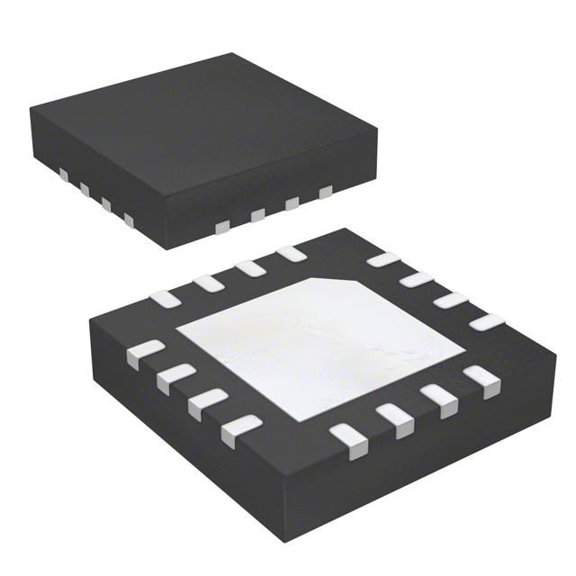
ICS844201I-45
16-Lead VFQFN
3mm x 3mm x 0.925mm package body
K Package
Top View
ICS844201BKI-45 REVISION A OCTOBER 7, 2013
1
©2013 Integrated Device Technology, Inc.
�FEMTOCLOCK® CRYSTAL-TO-LVDS CLOCK GENERATOR
ICS844201I-45 Data Sheet
Pin Descriptions and Characteristics
Table 1. Pin Descriptions
Number
Name
Type
Description
1, 6, 7, 8, 9,
13, 14, 15
nc
Unused
2,
3
XTAL_OUT
XTAL_IN
Input
4
FSEL
Input
5, 16
GND
Power
Power supply ground.
10
VDD
Power
Power supply pin.
11, 12
nQ, Q
Output
Differential output pair. LVDS interface levels.
No connect.
Crystal oscillator interface. XTAL_IN is the input, XTAL_OUT is the output.
Pullup
Frequency select pin. LVCMOS/LVTTL interface levels.
NOTE: Pullup refers to internal input resistors. See Table 2, Pin Characteristics, for typical values.
Table 2. Pin Characteristics
Symbol
Parameter
Test Conditions
Minimum
Typical
Maximum
Units
CIN
Input Capacitance
4
pF
RPULLUP
Input Pullup Resistor
51
k
Absolute Maximum Ratings
NOTE: Stresses beyond those listed under Absolute Maximum Ratings may cause permanent damage to the device. These ratings are stress
specifications only. Functional operation of the product at these conditions or any conditions beyond those listed in the DC Characteristics or
AC Characteristics is not implied. Exposure to absolute maximum rating conditions for extended periods may affect product reliability.
Item
Rating
Supply Voltage, VDD
4.6V
Inputs, VI
XTAL_IN
Other Inputs
0V to VDD
-0.5V to VDD + 0.5V
Outputs, IO
Continuous Current
Surge Current
10mA
15mA
Package Thermal Impedance, JA
74.9C/W (0 mps)
Storage Temperature, TSTG
-65C to 150C
ICS844201BKI-45 REVISION A OCTOBER 7, 2013
2
©2013 Integrated Device Technology, Inc.
�FEMTOCLOCK® CRYSTAL-TO-LVDS CLOCK GENERATOR
ICS844201I-45 Data Sheet
DC Electrical Characteristics
Table 3A. Power Supply DC Characteristics, VDD = 3.3V ± 10%, TA = -40°C to 85°C
Symbol
Parameter
VDD
Power Supply Voltage
IDD
Power Supply Current
Test Conditions
Minimum
Typical
Maximum
Units
2.97
3.3
3.63
V
95
mA
Maximum
Units
Table 3B. LVCMOS/LVTTL DC Characteristics, VDD = 3.3V ± 10%, TA = -40°C to 85°C
Symbol
Parameter
Test Conditions
Minimum
Typical
VIH
Input High Voltage
2
VDD + 0.3
V
VIL
Input Low Voltage
-0.3
0.8
V
IIH
Input High Current
VDD = VIN = 3.63V
5
µA
IIL
Input Low Current
VDD = 3.63V, VIN = 0V
-150
µA
Table 3C. LVDS DC Characteristics, VDD = 3.3V ± 10%, TA = -40°C to 85°C
Symbol
Parameter
VOD
Differential Output Voltage
VOD
VOD Magnitude Change
VDIFF_OUT
Peak-to-Peak Differential
Output Voltage
VOS
Offset Voltage
VOS
VOS Magnitude Change
Test Conditions
Minimum
Typical
Maximum
Units
454
mV
50
mV
494
908
mV
1.3
1.63
V
50
mV
Maximum
Units
34
MHz
Equivalent Series Resistance (ESR)
50
Shunt Capacitance
7
pF
247
Table 4. Crystal Characteristics
Parameter
Test Conditions
Minimum
Mode of Oscillation
Fundamental
Frequency
ICS844201BKI-45 REVISION A OCTOBER 7, 2013
Typical
24.5
3
25
©2013 Integrated Device Technology, Inc.
�FEMTOCLOCK® CRYSTAL-TO-LVDS CLOCK GENERATOR
ICS844201I-45 Data Sheet
AC Electrical Characteristics
Table 5. AC Characteristics, VDD = 3.3V ± 10%, TA = -40°C to 85°C
Symbol
Parameter
fOUT
Output Frequency
tjit(Ø)
tj
tREFCLK_HF_RMS
tREFCLK_LF_RMS
tR / tF
odc
RMS Phase Jitter,
Random; NOTE 1
Phase Jitter
Peak-to-Peak;
NOTE 2
Phase Jitter RMS;
NOTE 3
Phase Jitter RMS;
NOTE 3
Output Rise/Fall Time
Output Duty Cycle
Test Conditions
Minimum
Typical
Maximum
Units
125
MHz
100
MHz
125MHz, Integration Range:
12kHz – 20MHz
0.773
ps
100MHz, Integration Range:
12kHz – 20MHz
0.792
ps
125MHz, (1.2MHz – 21.9MHz)
25MHz crystal input
Evaluation Band: 0Hz - Nyquist
(clock frequency/2)
12.51
ps
100MHz, (1.2MHz – 21.9MHz)
25MHz crystal input
Evaluation Band: 0Hz - Nyquist
(clock frequency/2)
13.48
ps
125MHz, (1.2MHz – 21.9MHz)
25MHz crystal input
High Band: 1.5MHz - Nyquist
(clock frequency/2)
1.13
ps
100MHz, (1.2MHz – 21.9MHz)
25MHz crystal input
High Band: 1.5MHz - Nyquist
(clock frequency/2)
1.25
ps
125MHz, (1.2MHz – 21.9MHz)
25MHz crystal input
Low Band: 10kHz - 1.5MHz
0.32
ps
100MHz, (1.2MHz – 21.9MHz)
25MHz crystal input
Low Band: 10kHz - 1.5MHz
0.33
ps
20% to 80%
250
450
ps
fOUT = 125MHz
48
52
%
fOUT = 100MHz
46
54
%
NOTE: Electrical parameters are guaranteed over the specified ambient operating temperature range, which is established when the device is
mounted in a test socket with maintained transverse airflow greater than 500 lfpm. The device will meet specifications after thermal equilibrium
has been reached under these conditions.
NOTE: Characterized using a 25MHz crystal.
NOTE 1: Refer to Phase Noise Plots.
NOTE 2: Peak-to-Peak jitter after applying system transfer function for the Common Clock Architecture. Maximum limit for PCI Express Gen 1
is 86ps peak-to-peak for a sample size of 106 clock periods. See IDT Application Note PCI Express Reference Clock Requirements and also
the PCI Express Application section of this datasheet which show each individual transfer function and the overall composite transfer function.
NOTE 3: RMS jitter after applying the two evaluation bands to the two transfer functions defined in the Common Clock Architecture and
reporting the worst case results for each evaluation band. Maximum limit for PCI Express Generation 2 is 3.1ps rms for tREFCLK_HF_RMS
(High Band) and 3.0 ps RMS for tREFCLK_LF_RMS (Low Band). See IDT Application Note PCI Express Reference Clock Requirements and also
the PCI Express Application section of this datasheet which show each individual transfer function and the overall composite transfer function.
ICS844201BKI-45 REVISION A OCTOBER 7, 2013
4
©2013 Integrated Device Technology, Inc.
�FEMTOCLOCK® CRYSTAL-TO-LVDS CLOCK GENERATOR
ICS844201I-45 Data Sheet
Typical Phase Noise at 100MHz
Noise Power (dBc/Hz)
100MHz
RMS Phase Jitter (Random)
12kHz to 20MHz = 0.792ps (typical)
Offset Frequency (Hz)
Typical Phase Noise at 125MHz
Noise Power (dBc/Hz)
125MHz
RMS Phase Jitter (Random)
12kHz to 20MHz = 0.773ps (typical)
Offset Frequency (Hz)
ICS844201BKI-45 REVISION A OCTOBER 7, 2013
5
©2013 Integrated Device Technology, Inc.
�FEMTOCLOCK® CRYSTAL-TO-LVDS CLOCK GENERATOR
ICS844201I-45 Data Sheet
Parameter Measurement Information
SCOPE
Qx
VDD
3.3V±10%
POWER SUPPLY
+ Float GND –
nQx
3.3V LVDS Output Load AC Test Circuit
RMS Phase Jitter
nQ
nQ
80%
Q
80%
VOD
Q
20%
20%
tR
tF
Output Rise/Fall Time
Output Duty Cycle/Pulse Width/Period
Offset Voltage Setup
Differential Output Voltage Setup
VOD
VDIFF_OUT
380mV
(typical)
760mV
(typical)
Differential Output Voltage
ICS844201BKI-45 REVISION A OCTOBER 7, 2013
6
©2013 Integrated Device Technology, Inc.
�FEMTOCLOCK® CRYSTAL-TO-LVDS CLOCK GENERATOR
ICS844201I-45 Data Sheet
Application Information
Crystal Input Interface
The ICS844201I-45 has been characterized with 18pF parallel
resonant crystals. The capacitor values, C1 and C2, shown in Figure
1 below were determined using a 25MHz, 18pF parallel resonant
crystal and were chosen to minimize the ppm error. The optimum C1
and C2 values can be slightly adjusted for different board layouts.
XTAL_IN
C1
27pF
X1
18pF Parallel Crystal
XTAL_OUT
C2
27pF
Figure 1. Crystal Input Interface
ICS844201BKI-45 REVISION A OCTOBER 7, 2013
7
©2013 Integrated Device Technology, Inc.
�FEMTOCLOCK® CRYSTAL-TO-LVDS CLOCK GENERATOR
ICS844201I-45 Data Sheet
Overdriving the XTAL Interface
The XTAL_IN input can be overdriven by an LVCMOS driver or by one
side of a differential driver through an AC coupling capacitor. The
XTAL_OUT pin can be left floating. The amplitude of the input signal
should be between 500mV and 1.8V and the slew rate should not be
less than 0.2V/ns. For 3.3V LVCMOS inputs, the amplitude must be
reduced from full swing to at least half the swing in order to prevent
signal interference with the power rail and to reduce internal noise.
Figure 2A shows an example of the interface diagram for a high
speed 3.3V LVCMOS driver. This configuration requires that the sum
of the output impedance of the driver (Ro) and the series resistance
(Rs) equals the transmission line impedance. In addition, matched
termination at the crystal input will attenuate the signal in half. This
VCC
can be done in one of two ways. First, R1 and R2 in parallel should
equal the transmission line impedance. For most 50 applications,
R1 and R2 can be 100. This can also be accomplished by removing
R1 and changing R2 to 50. The values of the resistors can be
increased to reduce the loading for a slower and weaker LVCMOS
driver. Figure 2B shows an example of the interface diagram for an
LVPECL driver. This is a standard LVPECL termination with one side
of the driver feeding the XTAL_IN input. It is recommended that all
components in the schematics be placed in the layout. Though some
components might not be used, they can be utilized for debugging
purposes. The datasheet specifications are characterized and
guaranteed by using a quartz crystal as the input.
XTAL_OUT
R1
100
Ro
Rs
C1
Zo = 50 ohms
XTAL_IN
R2
100
Zo = Ro + Rs
.1uf
LVCMOS Driver
Figure 2A. General Diagram for LVCMOS Driver to XTAL Input Interface
XTAL_OUT
C2
Zo = 50 ohms
XTAL_IN
.1uf
Zo = 50 ohms
LVPECL Driver
R1
50
R2
50
R3
50
Figure 2B. General Diagram for LVPECL Driver to XTAL Input Interface
ICS844201BKI-45 REVISION A OCTOBER 7, 2013
8
©2013 Integrated Device Technology, Inc.
�FEMTOCLOCK® CRYSTAL-TO-LVDS CLOCK GENERATOR
ICS844201I-45 Data Sheet
LVDS Driver Termination
For a general LVDS interface, the recommended value for the
termination impedance (ZT) is between 90 and 132. The actual
value should be selected to match the differential impedance (Z0) of
your transmission line. A typical point-to-point LVDS design uses a
100 parallel resistor at the receiver and a 100 differential
transmission-line environment. In order to avoid any
transmission-line reflection issues, the components should be
surface mounted and must be placed as close to the receiver as
possible. IDT offers a full line of LVDS compliant devices with two
types of output structures: current source and voltage source. The
LVDS
Driver
standard termination schematic as shown in Figure 3A can be used
with either type of output structure. Figure 3B, which can also be
used with both output types, is an optional termination with center tap
capacitance to help filter common mode noise. The capacitor value
should be approximately 50pF. If using a non-standard termination, it
is recommended to contact IDT and confirm if the output structure is
current source or voltage source type. In addition, since these
outputs are LVDS compatible, the input receiver’s amplitude and
common-mode input range should be verified for compatibility with
the output.
ZO ZT
ZT
LVDS
Receiver
Figure 3A. Standard Termination
LVDS
Driver
ZO ZT
C
ZT
2 LVDS
ZT Receiver
2
Figure 3B. Optional Termination
LVDS Termination
ICS844201BKI-45 REVISION A OCTOBER 7, 2013
9
©2013 Integrated Device Technology, Inc.
�FEMTOCLOCK® CRYSTAL-TO-LVDS CLOCK GENERATOR
ICS844201I-45 Data Sheet
PCI Express Application Note
PCI Express jitter analysis methodology models the system
response to reference clock jitter. The block diagram below shows the
most frequently used Common Clock Architecture in which a copy of
the reference clock is provided to both ends of the PCI Express Link.
In the jitter analysis, the transmit (Tx) and receive (Rx) serdes PLLs
are modeled as well as the phase interpolator in the receiver. These
transfer functions are called H1, H2, and H3 respectively. The overall
system transfer function at the receiver is:
Ht s = H3 s H1 s – H2 s
The jitter spectrum seen by the receiver is the result of applying this
system transfer function to the clock spectrum X(s) and is:
Y s = X s H3 s H1 s – H2 s
In order to generate time domain jitter numbers, an inverse Fourier
Transform is performed on X(s)*H3(s) * [H1(s) - H2(s)].
PCIe Gen 2A Magnitude of Transfer Function
PCI Express Common Clock Architecture
For PCI Express Gen 1, one transfer function is defined and the
evaluation is performed over the entire spectrum: DC to Nyquist (e.g
for a 100MHz reference clock: 0Hz – 50MHz) and the jitter result is
reported in peak-peak.
PCIe Gen 2B Magnitude of Transfer Function
For PCI Express Gen 3, one transfer function is defined and the
evaluation is performed over the entire spectrum. The transfer
function parameters are different from Gen 1 and the jitter result is
reported in RMS.
PCIe Gen 1 Magnitude of Transfer Function
For PCI Express Gen 2, two transfer functions are defined with 2
evaluation ranges and the final jitter number is reported in rms. The
two evaluation ranges for PCI Express Gen 2 are 10kHz – 1.5MHz
(Low Band) and 1.5MHz – Nyquist (High Band). The plots show the
individual transfer functions as well as the overall transfer function Ht.
ICS844201BKI-45 REVISION A OCTOBER 7, 2013
PCIe Gen 3 Magnitude of Transfer Function
For a more thorough overview of PCI Express jitter analysis
methodology, please refer to IDT Application Note PCI Express
Reference Clock Requirements.
10
©2013 Integrated Device Technology, Inc.
�FEMTOCLOCK® CRYSTAL-TO-LVDS CLOCK GENERATOR
ICS844201I-45 Data Sheet
Schematic Example
Q
GN D
nc
nc
nc
U1
layouts, the C1 and C2 may be slightly adjusted for optimizing
frequency accuracy. Two examples of LVDS for receiver without
built-in termination are shown in this schematic.
16
15
14
13
Figure 4 shows an example of ICS844201I-45 application schematic.
In this example, the device is operated at VDD = 3.3V. The 18pF
parallel resonant 25MHz crystal is used. The C1 = 27pF and C2 =
27pF are recommended for frequency accuracy. For different board
F
p
8
1
25 MHz
C2
27pF
X1
XTAL_OUT
XTAL_IN
FSEL
1
2
3
4
nc
XTAL_OUT
XTAL_IN
FSEL
R1
100
12
11
10
9
nQ
+
-
Zo = 50 Ohm
VDD
GN D
nc
nc
nc
C1
27pF
Q
nQ
VDD
nc
Zo = 50 Ohm
5
6
7
8
C3
0.01u
VDD=3.3V
Logic Input Pin Examples
Set Logic
Input to
'1'
VDD
RU1
1K
Set Logic
Input to
'0'
VDD
Q
Zo = 50 Ohm
RU2
Not Install
To Logic
Input
pins
RD1
Not Install
R3
50
To Logic
Input
pins
RD2
1K
nQ
Zo = 50 Ohm
C9
0.1uF
R4
50
+
-
Alternate
LVDS
Termination
Figure 4. ICS844201I-45 Schematic Example
ICS844201BKI-45 REVISION A OCTOBER 7, 2013
11
©2013 Integrated Device Technology, Inc.
�FEMTOCLOCK® CRYSTAL-TO-LVDS CLOCK GENERATOR
ICS844201I-45 Data Sheet
Power Considerations
This section provides information on power dissipation and junction temperature for the ICS844201I-45.
Equations and example calculations are also provided.
1.
Power Dissipation.
The total power dissipation for the ICS844201I-45 is the sum of the core power plus the power dissipation in the load(s).
The following is the power dissipation for VDD = 3.3V + 10% = 3.63V, which gives worst case results.
•
Power (core)MAX = VDD_MAX * IDD_MAX = 3.63V * 95mA = 344.85mW
2. Junction Temperature.
Junction temperature, Tj, is the temperature at the junction of the bond wire and bond pad, and directly affects the reliability of the device. The
maximum recommended junction temperature is 125°C. Limiting the internal transistor junction temperature, Tj, to 125°C ensures that the bond
wire and bond pad temperature remains below 125°C.
The equation for Tj is as follows: Tj = JA * Pd_total + TA
Tj = Junction Temperature
JA = Junction-to-Ambient Thermal Resistance
Pd_total = Total Device Power Dissipation (example calculation is in section 1 above)
TA = Ambient Temperature
In order to calculate junction temperature, the appropriate junction-to-ambient thermal resistance JA must be used. Assuming no air flow and
a multi-layer board, the appropriate value is 74.9°C/W per Table 6 below.
Therefore, Tj for an ambient temperature of 85°C with all outputs switching is:
85°C + 0.345W * 74.9°C/W = 110.8°C. This is below the limit of 125°C.
This calculation is only an example. Tj will obviously vary depending on the number of loaded outputs, supply voltage, air flow and the type of
board (multi-layer).
Table 6. Thermal Resistance JA for 16 Lead VFQFN, Forced Convection
JA vs. Air Flow
Meters per Second
Multi-Layer PCB, JEDEC Standard Test Boards
ICS844201BKI-45 REVISION A OCTOBER 7, 2013
0
1
2.5
74.9°C/W
65.5°C/W
58.8°C/W
12
©2013 Integrated Device Technology, Inc.
�FEMTOCLOCK® CRYSTAL-TO-LVDS CLOCK GENERATOR
ICS844201I-45 Data Sheet
Reliability Information
Table 7. JA vs. Air Flow Table for a 16 Lead VFQFN
JA vs. Air Flow
Meters per Second
Multi-Layer PCB, JEDEC Standard Test Boards
0
1
2.5
74.9°C/W
65.5°C/W
58.8°C/W
Transistor Count
The transistor count for ICS844201I-45 is: 1986
ICS844201BKI-45 REVISION A OCTOBER 7, 2013
13
©2013 Integrated Device Technology, Inc.
�FEMTOCLOCK® CRYSTAL-TO-LVDS CLOCK GENERATOR
ICS844201I-45 Data Sheet
Package Outline and Package Dimensions
Package Outline - K Suffix for 16 Lead VFQFN
(Ref.)
Seating Plane
ND & NE
Even
(ND-1)x e
(R ef.)
A1
Index Area
A3
N
N
e (Typ.)
2 If ND & NE
1
Anvil
Singulation
or
Sawn
Singulation
Top View
L
are Even
2
E2
(NE -1)x e
(Re f.)
E2
2
b
A
(Ref.)
D
e
D2
2
ND & NE
Odd
0. 08
Chamfer 4x
0.6 x 0.6 max
OPTIONAL
C
Thermal
Base
D2
C
Bottom View w/Type A ID
Bottom View w/Type C ID
2
1
2
1
CHAMFER
4
RADIUS
N N-1
4
N N-1
There are 2 methods of indicating pin 1 corner at the back of the VFQFN package:
1. Type A: Chamfer on the paddle (near pin 1)
2. Type C: Mouse bite on the paddle (near pin 1)
Table 8. Package Dimensions
Symbol
N
A
A1
A3
b
ND & NE
D&E
D2 & E2
e
L
Reference Document: JEDEC Publication 95, MO-220
JEDEC Variation: VEED-2/-4
All Dimensions in Millimeters
Minimum
Maximum
16
0.80
1.00
0
0.05
0.25 Ref.
0.18
0.30
4
3.00 Basic
1.00
1.80
0.50 Basic
0.30
0.50
ICS844201BKI-45 REVISION A OCTOBER 7, 2013
14
©2013 Integrated Device Technology, Inc.
�FEMTOCLOCK® CRYSTAL-TO-LVDS CLOCK GENERATOR
ICS844201I-45 Data Sheet
Ordering Information
Table 9. Ordering Information
Part/Order Number
844201BKI-45LF
844201BKI-45LFT
Marking
B15L
B15L
ICS844201BKI-45 REVISION A OCTOBER 7, 2013
Package
“Lead-Free” 16 Lead VFQFN
“Lead-Free” 16 Lead VFQFN
15
Shipping Packaging
Tube
Tape & Reel
Temperature
-40C to 85C
-40C to 85C
©2013 Integrated Device Technology, Inc.
�FEMTOCLOCK® CRYSTAL-TO-LVDS CLOCK GENERATOR
ICS844201I-45 Data Sheet
We’ve Got Your Timing Solution
6024 Silver Creek Valley Road
San Jose, California 95138
Sales
800-345-7015 (inside USA)
+408-284-8200 (outside USA)
Fax: 408-284-2775
www.IDT.com/go/contactIDT
Technical Support Sales
netcom@idt.com
+480-763-2056
DISCLAIMER Integrated Device Technology, Inc. (IDT) and its subsidiaries reserve the right to modify the products and/or specifications described herein at any time and at IDT’s sole discretion. All information in this document,
including descriptions of product features and performance, is subject to change without notice. Performance specifications and the operating parameters of the described products are determined in the independent state and are not
guaranteed to perform the same way when installed in customer products. The information contained herein is provided without representation or warranty of any kind, whether express or implied, including, but not limited to, the
suitability of IDT’s products for any particular purpose, an implied warranty of merchantability, or non-infringement of the intellectual property rights of others. This document is presented only as a guide and does not convey any
license under intellectual property rights of IDT or any third parties.
IDT’s products are not intended for use in applications involving extreme environmental conditions or in life support systems or similar devices where the failure or malfunction of an IDT product can be reasonably expected to significantly affect the health or safety of users. Anyone using an IDT product in such a manner does so at their own risk, absent an express, written agreement by IDT.
Integrated Device Technology, IDT and the IDT logo are registered trademarks of IDT. Other trademarks and service marks used herein, including protected names, logos and designs, are the property of IDT or their respective third
party owners.
Copyright 2013. All rights reserved.
�