DATA SHEET
FemtoClock® NG Universal Frequency
Translator
IDT8T49N222I
General Description
Features
The IDT8T49N222I is a highly flexible FemtoClock® NG general
purpose, low phase noise Frequency Translator / Synthesizer with
alarm and monitoring functions suitable for networking and
communications applications. It is able to generate any output
frequency in the 7.29MHz to 833.33MHz range and most output
frequencies in the 925MHz to 1200MHz range (see Table 3A for
details). A wide range of input reference clocks and a range of
low-cost fundamental mode crystal frequencies may be used as the
source for the output frequency.
•
•
Fourth generation FemtoClock® NG technology
Universal Frequency Translator
• Zero ppm frequency translation
•
Two outputs, individually programmable as LVPECL or LVDS
• Outputs may be individually set to use 2.5V or 3.3V output
levels
• Individually programmable output frequencies: 7.29MHz up to
1200MHz
Two differential inputs support the following input types:
LVPECL, LVDS, LVHSTL, HCSL
• Input frequency range: 8kHz to 710MHz
• Hitless switching between inputs
Crystal input frequency range: 16MHz to 40MHz
• Holdover support in the event both inputs fail
One factory-set register configuration for power-up default state
• Configurations customized via One-Time Programmable ROM
• Settings may be overwritten after power-up via I2C
• I2C Serial interface for register programming
RMS phase jitter at 156.25MHz, using a 40MHz crystal
(12kHz - 20MHz): 507fs (typical), Low Bandwidth Mode (FracN)
Supports ITU-T G.8262 Synchronous Ethernet equipment slave
clocks (EEC option 1 and 2)
Output supply voltage modes:
VCC/VCCA/VCCOx
3.3V/3.3V/3.3V
3.3V/3.3V/2.5V (LVPECL only)
2.5V/2.5V/2.5V
•
The IDT8T49N222I has three operating modes to support a very
broad spectrum of applications:
1) Frequency Synthesizer
•
Synthesizes output frequencies from a 16MHz - 40MHz
fundamental mode crystal.
•
•
Fractional feedback division is used, so there are no
requirements for any specific crystal frequency to produce the
desired output frequency with a high degree of accuracy.
•
2) High-Bandwidth Frequency Translator
•
•
3) Low-Bandwidth Frequency Translator
Applications: Networking & Communications.
•
This mode supports PLL loop bandwidths in the 10Hz - 580Hz
range and makes use of an external crystal to provide
significant jitter attenuation.
Translates any input clock in the 8kHz –710MHz frequency
range into any supported output frequency.
•
•
-40°C to 85°C ambient operating temperature
Available in lead-free (RoHS 6) package
Pin Assignment
VCCO0
This device provides a factory-programmed default power-up
configuration burned into One-Time Programmable (OTP) memory.
The configuration is specified by the customer and is programmed by
IDT during the final test phase from an on-hand stock of blank
devices.
CLK_ACTIVE
VEE
LF0
LF1
VEE
VEE
nc
VCCA
HOLDOVER
CLK0BAD
To implement other configurations, these power-up default settings
can be overwritten after power-up using the I2C interface and the
device can be completely reconfigured. However, these settings
would have to be written every time the device powers-up.
CLK1BAD
36 35 34 33 32 31 30 29 28 27 26 25
37
24
38
23
39
22
IDT8T49N222I
40
21
48 Lead VFQFN
20
41
7.0mm x 7.0mm x 0.925mm,
42
19
package body
43
18
NL Package
44
17
Top View
45
16
46
15
47
14
48
13
1 2 3 4 5 6 7 8 9 10 11 12
XTAL_IN
XTALBAD
IDT8T49N222BNLGI REVISION A MAY 13, 2013
1
nQ1
VCCO1
•
•
VEE
nc
VCC
S_AO
S_A1
Reserved
nc
SCLK
SDATA
VCC
PLL_BYPASS
nc
CLK1
nCLK1
This mode has a high PLL loop bandwidth in order to track input
reference changes, such as Spread-Spectrum Clock
modulation, so it will not attenuate much jitter on the input
reference.
OE1
VEE
Q1
•
•
Translates any input clock in the 16MHz - 710MHz frequency
range into any supported output frequency.
Q0
nQ0
VEE
OE0
LOCK_IND
VEE
Applications: PCI Express, Computing, General Purpose
XTAL_OUT
VCC
CLK_SEL
CLK0
nCLK0
VCC
nc
VEE
VEE
•
•
©2013 Integrated Device Technology, Inc.
�IDT8T49N222I Data Sheet
FemtoClock® NG Universal Frequency Translator
Block Diagram
PLL_BYPASS
XTAL_IN
OSC
1
x2
PD/LF
XTAL_OUT
FemtoClock® NG
VCO
Output Divider
÷N0[7:0]
0
0
Q0
1
nQ0
OE0
Feedback Divider
÷M_INT
[7:0]
÷M_FRAC
[17:0]
÷N1[7:0]
0
Q1
1
nQ1
OE1
ADC
LF1
CLK_SEL
R3
÷4
CLK0
nCLK0
CLK1
nCLK1
0
÷M1[16:0]
PD/CP
LF0
C3
RS
÷P[16:0]
1
CP
Control Logic
OTP
POR
Status Indicators
CLK_ACTIVE
LOCK_IND
XTALBAD
CLK0BAD
CLK1BAD
HOLDOVER
Global Registers
Register Set
SCLK, S_A0, S_A1
IDT8T49N222BNLGI REVISION A MAY 13, 2013
CS
SDATA
2
©2013 Integrated Device Technology, Inc.
�IDT8T49N222I Data Sheet
FemtoClock® NG Universal Frequency Translator
Pin Descriptions and Pin Characteristic Tables
Table 1. Pin Descriptions
Number
Name
Type
1
2
XTAL_IN
XTAL_OUT
Input
Crystal Oscillator interface designed for 12pF parallel resonant crystals.
XTAL_IN (pin 1) is the input and XTAL_OUT (pin 2) is the output.
3, 7, 15, 22
VCC
Power
Core supply pins. All must be either 3.3V or 2.5V.
4
CLK_SEL
Input
Pulldown
Input clock select. Selects the active differential clock input.
0 = CLK0, nCLK0 (default)
1 = CLK1, nCLK1
5
CLK0
Input
Pulldown
Non-inverting differential clock input.
6
nCLK0
Input
Pullup/
Pulldown
Inverting differential clock input. VCC/2 default when left floating (set by the
internal pullup and pulldown resistors).
8, 13, 18,
23, 43
nc
Unused
9, 10, 24,
28, 30, 33,
38, 41, 42
VEE
Power
11
CLK1
Input
Pulldown
Non-inverting differential clock input.
12
nCLK1
Input
Pullup/
Pulldown
Inverting differential clock input. VCC/2 default when left floating (set by the
internal pullup and pulldown resistors).
14
PLL_BYPASS
Input
Pulldown
Bypasses the VCXO PLL.
0 = PLL Mode (default)
1 = PLL Bypassed
16
SDATA
I/O
Pullup
I2C Data Input/Output. Open drain.
17
SCLK
Input
Pullup
I2C Clock Input. LVCMOS/LVTTL Interface Levels.
19
Reserved
Unused
20
S_A1
Input
Pulldown
I2C Address Bit 1. LVCMOS/LVTTL Interface Levels.
21
S_A0
Input
Pulldown
I2C Address Bit 0. LVCMOS/LVTTL Interface Levels.
25
VCCO1
Power
Output supply pins for Q1, nQ1 outputs. Either 2.5V or 3.3V.
26, 27
nQ1, Q1
Output
Differential output. Output type is programmable to LVDS or LVPECL interface
levels.
29
OE1
Input
31
LOCK_IND
Output
32
OE0
Input
34, 35
nQ0, Q0
Output
Differential output. Output type is programmable to LVDS or LVPECL interface
levels.
36
VCCO0
Power
Output supply pins for Q0, nQ0 outputs. Either 2.5V or 3.3V.
37
CLK_ACTIVE
Output
Indicates which of the two differential clock inputs is currently selected.
0 = CLK0, nCLK0 differential input pair
1 = CLK1, nCLK1 differential input pair
39, 40
LF0, LF1
Input
IDT8T49N222BNLGI REVISION A MAY 13, 2013
Description
No connect. These pins are to be left unconnected.
Negative supply pins.
Must be left unconnected.
Pullup
Active High Output Enable for Q1, nQ1.
0 = Output pins high-impedance
1 = Output switching (default)
Lock Indicator - indicates that the PLL is in a locked condition. LVCMOS/LVTTL
interface levels.
Pullup
Active High Output Enable for Q0, nQ0.
0 = Output pins high-impedance
1 = Output switching (default)
Loop filter connection node pins. LF0 is the output. LF1 is the input.
3
©2013 Integrated Device Technology, Inc.
�IDT8T49N222I Data Sheet
FemtoClock® NG Universal Frequency Translator
Table 1. Pin Descriptions
Number
Name
Type
Description
Continued on next page.
44
VCCA
Power
Analog supply voltage.
45
HOLDOVER
Output
Alarm output reflecting if the device is in a holdover state. LVCMOS/LVTTL
interface levels.
0 = Device is locked to a valid input reference
1 = Device is not locked to a valid input reference
46
CLK0BAD
Output
Alarm output reflecting the state of CLK0. LVCMOS/LVTTL interface levels.
0 = Input Clock 0 is switching within specifications
1 = Input Clock 0 is out of specification
47
CLK1BAD
Output
Alarm output reflecting the state of CLK1. LVCMOS/LVTTL interface levels.
0 = Input Clock 1 is switching within specifications
1 = Input Clock 1 is out of specification
48
XTALBAD
Output
Alarm output reflecting the state of XTAL. LVCMOS/LVTTL interface levels.
0 = crystal is switching within specifications
1 = crystal is out of specification
NOTE: Pullup and Pulldown refer to internal input resistors. See Table 2, Pin Characteristics, for typical values.
Table 2. Pin Characteristics
Symbol
Parameter
CIN
Input Capacitance
3.5
pF
RPULLUP
Input Pullup Resistor
51
k
RPULLDOWN
Input Pulldown Resistor
51
k
ROUT
Output
Impedance
Test Conditions
Minimum
Typical
Maximum
Units
HOLDOVER,
CLK_ACTIVE,
CLK0BAD, CLK1BAD,
XTALBAD, LOCK_IND
VCC = 3.465V
25
HOLDOVER,
CLK_ACTIVE,
CLK0BAD, CLK1BAD,
XTALBAD, LOCK_IND
VCC = 2.625V
25
IDT8T49N222BNLGI REVISION A MAY 13, 2013
4
©2013 Integrated Device Technology, Inc.
�IDT8T49N222I Data Sheet
FemtoClock® NG Universal Frequency Translator
Functional Description
Operating Modes
The IDT8T49N222I is designed to provide two output frequencies
almost anywhere within its supported output frequency range
(7.29MHz to 1200MHz) from any input source in the supported input
frequency range (8kHz to 710MHz). It is capable of synthesizing
frequencies from a crystal or crystal oscillator source. The output
frequency is generated regardless of the relationship to the input
frequency. The output frequency will be exactly the required
frequency in most cases. In most others, it will only differ from the
desired frequency by a few ppb. IDT configuration software will
indicate the frequency error, if any. The IDT8T49N222I can translate
the desired output frequency from one of two input clocks. Again, no
relationship is required between the input and output frequencies in
order to translate to the output clock rate. In this frequency translation
mode, a low-bandwidth, jitter attenuation option is available that
makes use of an external fixed-frequency crystal or crystal oscillator
to translate from a noisy input source. If the input clock is known to
be fairly clean or if some modulation on the input needs to be tracked,
then the high-bandwidth frequency translation mode can be used,
without the need for the external crystal.
The IDT8T49N222I has three operating modes which are set by the
MODE_SEL[1:0] bits. There are two frequency translator modes low bandwidth and high bandwidth and a frequency synthesizer
mode.
Please make use of IDT-provided configuration applications to
determine the best operating settings for the desired configurations
of the device.
Output Dividers & Supported Output Frequencies
The internal VCO is capable of operating in a range from 1.850GHz
up to 2.5GHz. The output divider stages N0[7:0] and N1[7:0] are
limited to selection of integers from 2 to 254. Please refer to Table 3A
for the recommended values of N applicable to the desired output
frequency.
Table 3A. Output Divider Settings & Frequency Ranges*
The input clock references and crystal input are monitored
continuously and appropriate alarms are raised both as register bits
and hard-wired pins in the event of any out-of-specification conditions
arising. Clock switching is supported in manual, revertive &
non-revertive modes.
Register
Setting
Frequency
Divider
Minimum
fOUT
Maximum
fOUT
Nn[7:0]
Nn
(MHz)
(MHz)
0000000x
Not Supported
00000010
2
925.00
1200.00
The IDT8T49N222I has one factory-programmed configuration that
sets the default operating state after reset. These defaults may be
over-written by I2C register access at any time, but those over-written
settings will be lost on power-down. Please contact IDT if a specific
set of power-up default settings is desired. Users that have a custom
configuration programmed may not require I2C access.
00000011
3
616.67
833.33
00000100
4
462.50
625.00
00000101
5
370.00
500.00
00000110
6
308.33
416.67
00000111
7
264.29
357.14
Please make use of IDT-provided configuration tools to determine the
best operating settings for the desired configurations of the device.
Please refer to the Universal Frequency Translator Family
Programming Guide if further details are required.
00001000
8
231.25
312.50
00001001
9
205.56
277.78
00001010
10
185.00
250.00
7.29
9.84
...
11111110
254
*NOTE: Frequency ranges for other N output dividers are possible.
Contact IDT Factory for special cases.
In addition to the above output divider settings, it is possible for either
or both of the outputs to present a copy of the currently active input
reference frequency by asserting the appropriate BYPn register bit.
IDT8T49N222BNLGI REVISION A MAY 13, 2013
5
©2013 Integrated Device Technology, Inc.
�IDT8T49N222I Data Sheet
FemtoClock® NG Universal Frequency Translator
Frequency Synthesizer Mode
Below are some example configurations for some common frequency
combinations. Please use the IDT Configuration SW or consult with
IDT to select other options.
This mode of operation allows an arbitrary output frequency to be
generated from a fundamental mode crystal input. For improved
phase noise performance, the crystal input frequency may be doubled. As can be seen from the block diagram in Figure 1, only the upper feedback loop is used in this mode of operation. It is recommended that CLK0 and CLK1 be left unused in this mode of operation.
Table 3B. Common Frequency Combination Examples
Output Frequency
(MHz)
Output Divider
Ratio
125
15
156.25
12
25
75
156.25
12
25
80
125
16
155.52
12
622.08
3
VCO Operating
Frequency (MHz)
The upper feedback loop supports a delta-sigma fractional feedback
divider. This allows the VCO operating frequency to be a non-integer
multiple of the crystal frequency. By using an integer multiple only,
lower phase noise jitter on the output can be achieved, however the
use of the delta-sigma divider logic will provide excellent performance on the output if a fractional divisor is used.
1875
1875
2000
PLL_BYPASS
1866.24
XTAL
96
622.08
3
161.1328125
12
644.53125
3
156.25
12
625
3
122.88
20
614.4
4
245.76
10
614.4
4
30.72
80
614.4
4
153.6
16
614.4
4
15.36
144
737.28
3
125
16
133.3333
15
32.76
60
OSC
x2
PD/LF
FemtoClock® NG
VCO
15
26.5625
80
212.5
10
106.25
18
318.75
6
nQ0
Feedback Divider
÷M_INT
[7:0]
Q1
÷M_FRAC
[17:0]
÷N1[7:0]
nQ1
1933.59375
OE1
1875
POR
2457.6
2457.6
Status Indicators
Control Logic
Global Registers
LOCK_IND
XTALBAD
Register Set
SDATA
SCLK, S_A0, S_A1
Figure 1. Frequency Synthesizer Mode Block Diagram
2457.6
High-Bandwidth Frequency Translator Mode
This mode of operation is used to translate one of two input clocks of
the same nominal frequency into an output frequency with little jitter
attenuation. As can be seen from the block diagram in Figure 2,
similarly to the Frequency Synthesizer mode, only the upper
feedback loop is used.
2457.6
2211.84
2000
PLL_BYPASS
Output Divider
1
131.04
Q0
÷N0[7:0]
0
OE0
1866.24
OTP
19.44
Output Divider
1
XTAL_IN
XTAL_OUT
1965.6
PD/LF
FemtoClock® NG
VCO
÷N0[7:0]
0
0
Q0
1
nQ0
OE0
Feedback Divider
÷M_INT
[7:0]
2125
÷M_FRAC
[17:0]
÷N1[7:0]
0
1
Q1
nQ1
OE1
1912.5
CLK_SEL
CLK0
nCLK0
CLK1
nCLK1
0
÷P[16:0]
1
Control Logic
OTP
POR
Global Registers
Register Set
SCLK, S_A0, S_A1
Status Indicators
CLK_ACTIVE
LOCK_IND
CLK0BAD
CLK1BAD
HOLDOVER
SDATA
Figure 2. High Bandwidth Frequency Translator Mode
Block Diagram
IDT8T49N222BNLGI REVISION A MAY 13, 2013
6
©2013 Integrated Device Technology, Inc.
�IDT8T49N222I Data Sheet
FemtoClock® NG Universal Frequency Translator
The input reference frequency range is now extended up to 710MHz.
A pre-divider stage P is needed to keep the operating frequencies at
the phase detector below 100MHz.
CLK0BAD - indicates if valid edges are being received on the CLK0
reference input. Detection is performed by comparing the input to the
feedback signal at the appropriate Phase / Frequency Detector
(PFD). When operating in high-bandwidth mode, the feedback at the
upper PFD is used. In low-bandwidth mode, the feedback at the lower
PFD is used. If three edges are received on the feedback without an
edge on the CLK0 reference input, the CLK0BAD alarm is asserted
on the pin & register bit. Once an edge is detected on the CLK0
reference input, the alarm is deasserted.
Low-Bandwidth Frequency Translator Mode
As can be seen from the block diagram in Figure 3, this mode
involves two PLL loops. The lower loop with the large integer dividers
is the low bandwidth loop and it sets the output-to-input frequency
translation ratio.This loop drives the upper DCXO loop (digitally
controlled crystal oscillator) via an analog-digital converter.
CLK1BAD - indicates if valid edges are being received on the CLK1
reference input. Behavior is as indicated for the CLK0BAD alarm, but
with the CLK1 input being monitored and the CLK1BAD output pin &
register bits being affected.
PLL_BYPASS
XTAL
1
XTAL_IN
XTAL_OUT
OSC
x2
PD/LF
FemtoClock® NG
VCO
Output Divider
÷N0[7:0]
0
0
Q0
1
nQ0
HOLDOVER - indicates that the device is not locked to a valid input
reference clock. This can occur in Manual switchover mode if the
selected reference input has gone bad, even if the other reference
input is still good. In automatic mode, this will only assert if both input
references are bad.
OE0
Feedback Divider
÷M_INT
[7:0]
÷M_FRAC
[17:0]
÷N1[7:0]
Q1
0
1
nQ1
OE1
ADC
LF1
CLK_SEL
R3
÷4
CLK0
nCLK0
CLK1
nCLK1
0
÷M1[16:0]
PD/CP
LF0
C3
RS
Input Reference Selection and Switching
÷P[16:0]
1
CP
Control Logic
OTP
POR
Both input references CLK0 and CLK1 must be the same nominal frequency. These may be driven by any type of clock source, including
crystal oscillator modules. A difference in frequency may cause the
PLL to lose lock when switching between input references. Please
contact IDT for the exact limits for your situation.
Status Indicators
Global Registers
Register Set
SCLK, S_A0, S_A1
CS
CLK_ACTIVE
LOCK_IND
XTALBAD
CLK0BAD
CLK1BAD
HOLDOVER
SDATA
Figure 3. Low Bandwidth Frequency Translator Mode
Block Diagram
The global control bits AUTO_MAN[1:0] dictate the order of priority
and switching mode to be used between the CLK0 and CLK1 inputs.
The pre-divider stage is used to scale down the input frequency by
an integer value to achieve a frequency in this range. By dividing
down the fed-back VCO operating frequency by the integer divider
M1[16:0] to as close as possible to the same frequency, exact output
frequency translations can be achieved. The phase detector of the
lower loop is designed to work with frequencies in the 8kHz - 16kHz
range. For improved phase noise performance, the crystal input
frequency may be doubled.
Manual Switching Mode
When the AUTO_MAN[1:0] field is set to Manual via Pin, then the
IDT8T49N222I will use the CLK_SEL input pin to determine which input to use as a reference. Similarly, if set to Manual via Register, then
the device will use the CLK_SEL register bit to determine the input
reference. In either case, the PLL will lock to the selected reference
if there is a valid clock present on that input.
If there is not a valid clock present on the selected input, the
IDT8T49N222I will go into holdover state and the HOLDOVER alarm
will be raised. This will occur even if there is a valid clock on the
non-selected reference input. The device will recover from holdover
state once a valid clock is re-established on the selected reference
input.
Alarm Conditions & Status Bits
The IDT8T49N222I monitors a number of conditions and reports their
status via both output pins and register bits.
CLK_ACTIVE - indicates which input clock reference is being used to
derive the output frequency.
The IDT8T49N222I will only switch input references on command
from the user. The user must either change the CLK_SEL register bit
(if in Manual via Register) or CLK_SEL input pin (if in Manual via Pin).
LOCK_IND - This status is asserted on the pin & register bit when the
PLL is locked to the appropriate input reference for the chosen mode
of operation. The status bit will not assert until a stable lock has been
achieved, but will de-assert once lock is lost.
Automatic Switching Mode
When the AUTO_MAN[1:0] field is set to either of the automatic
selection modes (Revertive or Non-Revertive), the IDT8T49N222I
determines which input reference it prefers / starts from by the state
of the CLK_SEL register bit only. The CLK_SEL input pin is not used
in either Automatic switching mode.
XTALBAD - indicates if valid edges are being received on the crystal
input. Detection is performed by comparing the input to the feedback
signal at the upper loop’s Phase / Frequency Detector (PFD). If three
edges are received on the feedback without an edge on the crystal
input, the XTALBAD alarm is asserted on the pin & register bit. Once
an edge is detected on the crystal input, the alarm is immediately
deasserted.
IDT8T49N222BNLGI REVISION A MAY 13, 2013
When starting from an unlocked condition, the device will lock to the
input reference indicated by the CLK_SEL register bit. It will not pay
7
©2013 Integrated Device Technology, Inc.
�IDT8T49N222I Data Sheet
FemtoClock® NG Universal Frequency Translator
Holdover / Free-run Behavior
attention to the non-selected input reference until a locked state has
been achieved. This is necessary to prevent ‘hunting’ behavior during
the locking phase.
When both input references have failed (Automatic mode) or the
selected input has failed (Manual mode), the IDT8T49N222I will
enter holdover (Low Bandwidth Frequency Translator mode) or
free-run (High Bandwidth Frequency Translator mode) state if. In
both cases, once the input reference is lost, the PLL will stop making
adjustments to the output phase.
Once the IDT8T49N222I has achieved a stable lock, it will remain
locked to the preferred input reference as long as there is a valid clock
on it. If at some point, that clock fails, then the device will automatically switch to the other input reference as long as there is a valid
clock there. If there is not a valid clock on either input reference, the
IDT8T49N222I will go into holdover state and the HOLDOVER alarm
will be raised.
If operating in Low Bandwidth Frequency Translation mode, the PLL
will continue to reference itself to the local oscillator and will hold its
output phase and frequency in relation to that source. Output stability
is determined by the stability of the local oscillator in this case.
The device will recover from holdover state once a valid clock is
re-established on either reference input. If clocks are valid on both
input references, the device will choose the reference indicated by
the CLK_SEL register bit.
However, if operating in High Bandwidth Frequency Translation
mode, the PLL no longer has any frequency reference to use and
output stability is now determined by the stability of the internal VCO.
If running from the non-preferred input reference and a valid clock
returns, there is a difference in behavior between Revertive and
Non-revertive modes. In Revertive mode, the device will switch back
to the reference indicated by the CLK_SEL register bit even if there
is still a valid clock on the non-preferred reference input. In
Non-revertive mode, the IDT8T49N222I will not switch back as long
as the non-preferred input reference still has a valid clock on it.
If the device is programmed to perform Manual switching, once the
selected input reference recovers, the IDT8T49N222I will switch back
to that input reference. If programmed for either Automatic mode, the
device will switch back to whichever input reference has a valid clock
first.
The switchover that results from returning from holdover or free-run
is handled in the same way as a switch between two valid input
references as described in the previous section.
Switchover Behavior of the PLL
Even though the two input references have the same nominal frequency, there may be minor differences in frequency and potentially
large differences in phase between them. The IDT8T49N222I will adjust its output to the new input reference. It will use Phase Slope Limiting to adjust the output phase at a fixed maximum rate until the
output phase and frequency are now aligned to the new input reference. Phase will always be adjusted by extending the clock period of
the output so that no unacceptably short clock periods are generated
on the output IDT8T49N222I.
IDT8T49N222BNLGI REVISION A MAY 13, 2013
8
©2013 Integrated Device Technology, Inc.
�IDT8T49N222I Data Sheet
FemtoClock® NG Universal Frequency Translator
Output Configuration
Serial Interface Configuration Description
The two outputs of the IDT8T49N222I provide separate output
frequencies. Each output may have a different output voltage level of
3.3V or 2.5V, although this output voltage must be less than or equal
to the core voltage (3.3V or 2.5V) the rest of the device is operating
from. The output voltage level used on each output is supplied on
their respective VCCO pin.
The IDT8T49N222I has an I2C-compatible configuration interface to
access any of the internal registers (Table 4D) for frequency and PLL
parameter programming. The IDT8T49N222I acts as a slave device
on the I2C bus and has the address 0b11011xx, where xx is set by the
values on the S_A0 & S_A1 pins (see Table 4A for details). The
interface accepts byte-oriented block write and block read
operations. An address byte (P) specifies the register address (Table
4D) as the byte position of the first register to write or read. Data
bytes (registers) are accessed in sequential order from the lowest to
the highest byte (most significant bit first, see table 4B, 4C). Read
and write block transfers can be stopped after any complete byte
transfer. It is recommended to terminate I2C the read or write transfer
after accessing byte #23.
The two outputs are individually selectable as LVDS or LVPECL
output types via the Qn_TYPE register bits (where n = 0 for Q0 / nQ0
and n = 1 for the Q1 / nQ1 output pair).
The two outputs can be enabled individually also via both register
control bits and input pins. When both the OEn register bit and OEn
pin are enabled, then the appropriate output is enabled. The OEn
register bits default to enabled so that by default the outputs can be
directly controlled by the input pins. Similarly, the input pins are
provisioned with weak pull-ups so that if they are left unconnected,
the output state can be directly controlled by the register bits. When
the differential output is in the disabled state, it will show a high
impedance condition.
For full electrical I2C compliance, it is recommended to use external
pull-up resistors for SDATA and SCLK. The internal pull-up resistors
have a size of 50k typical.
Note: if a different device slave address is desired, please
contact IDT.
Table 4A. I2C Device Slave Address
1
1
0
1
1
S_A1
S_A0
R/W
Table 4B. Block Write Operation
Bit
Description
1
2:8
9
10
11:18
19
20:27
28
29-36
37
...
...
...
START
Slave
Address
W (0)
ACK
Address
Byte (P)
ACK
Data Byte
(P)
ACK
Data Byte
(P+1)
ACK
Data Byte
...
ACK
STOP
1
7
1
1
8
1
8
1
8
1
8
1
1
Length (bits)
Table 4C. Block Read Operation
Bit
1
2:8
9
10
11:18
19
20
21:27
28
29
30:37
38
39-46
47
...
...
...
START
Slave
Address
W
(0)
A
C
K
Address
Byte (P)
A
C
K
Repeated
START
Slave
Address
R
(1)
A
C
K
Data Byte
(P)
A
C
K
Data Byte
(P+1)
A
C
K
Data Byte
...
A
C
K
STOP
1
7
1
1
8
1
1
7
1
1
8
1
8
1
8
1
1
Description
Length (bits)
IDT8T49N222BNLGI REVISION A MAY 13, 2013
9
©2013 Integrated Device Technology, Inc.
�IDT8T49N222I Data Sheet
FemtoClock® NG Universal Frequency Translator
Register Descriptions
Please consult IDT for configuration software and/or programming guides to assist in selection of optimal register settings for the desired
configurations.
Table 4D. I C Register Map
2
Register Bit
Reg
Binary
Regist
er
Addre
ss
D7
D6
D5
D4
D3
D2
D1
D0
0
00000
MFRAC[17]
MFRAC0[16]
MFRAC0[15]
MFRAC0[14]
MFRAC0[13]
MFRAC0[12]
MFRAC0[11]
MFRAC0[10]
1
00001
Rsvd
Rsvd
Rsvd
Rsvd
Rsvd
Rsvd
Rsvd
Rsvd
2
00010
MFRAC0[9]
MFRAC0[8]
MFRAC0[7]
MFRAC0[6]
MFRAC0[5]
MFRAC0[4]
MFRAC0[3]
MFRAC0[2]
3
00011
Rsvd
Rsvd
Rsvd
Rsvd
Rsvd
Rsvd
Rsvd
Rsvd
4
00100
MFRAC0[1]
MFRAC0[0]
MINT[7]
MINT[6]
MINT[5]
MINT[4]
MINT[3]
MINT[2]
5
00101
Rsvd
Rsvd
Rsvd
Rsvd
Rsvd
Rsvd
Rsvd
Rsvd
6
00110
MINT[1]
MINT[0]
P[16]
P[15]
P[14]
P[13]
P[12]
P[11]
7
00111
Rsvd
Rsvd
Rsvd
Rsvd
Rsvd
Rsvd
Rsvd
Rsvd
8
01000
P[10]
P[9]
P[8]
P[7]
P[6]
P[5]
P[4]
P[3]
9
01001
Rsvd
Rsvd
Rsvd
Rsvd
Rsvd
Rsvd
Rsvd
Rsvd
10
01010
P[2]
P[1]
P[0]
M1[16]
M1[15]
M1[14]
M1[13]
M1[12]
11
01011
Rsvd
Rsvd
Rsvd
Rsvd
Rsvd
Rsvd
Rsvd
Rsvd
12
01100
M1[11]
M1[10]
M1[9]
M1[8]
M1[7]
M1[6]
M1[5]
M1[4]
13
01101
Rsvd
Rsvd
Rsvd
Rsvd
Rsvd
Rsvd
Rsvd
Rsvd
14
01110
M1[3]
M1[2]
M1[1]
M1[0]
Rsvd
Rsvd
Rsvd
Rsvd
15
01111
Rsvd
Rsvd
Rsvd
Rsvd
Rsvd
Rsvd
Rsvd
Rsvd
16
10000
N0[7]
N0[6]
N0[5]
N0[4]
N0[3]
N0[2]
N0[1]
N0[0]
17
10001
N1[7]
N1[6]
N1[5]
N1[4]
N1[3]
N1[2]
N1[1]
N1[0]
18
10010
Rsvd
BW[6]
BW[5]
BW[4]
BW[3]
BW[2]
BW[1]
BW[0]
19
10011
DBL_XTAL
Re-Calibrate
OE1
OE0
Q1_TYPE
Q0_TYPE
BYP1
BYP0
20
10100
MODE_SEL1
MODE_SEL0
0
0
Rsvd
Rsvd
Rsvd
Rsvd
21
10101
CLK_SEL
AUTO_MAN[1]
AUTO_MAN[0]
0
ADC_RATE[1]
ADC_RATE[0]
LCK_WIN[1]
LCK_WIN[0]
22
10110
1
0
1
0
0
0
0
0
23
10111
CLK_ACTIVE
HOLDOVER
CLK1BAD
CLK0BAD
XTAL_BAD
LOCK_IND
Rsvd
Rsvd
IDT8T49N222BNLGI REVISION A MAY 13, 2013
10
©2013 Integrated Device Technology, Inc.
�IDT8T49N222I Data Sheet
FemtoClock® NG Universal Frequency Translator
Table 4E. Control Bits
Register Bits
Function
Q0_TYPE
Determines the output type for output pair Q0, nQ0.
0 = LVPECL (Default)
1 = LVDS
Q1_TYPE
Determines the output type for output pair Q1, nQ1.
0 = LVPECL (Default)
1 = LVDS
BYP0
Bypass Input to output Q0.
0 = Use result of output divider N0 (Default)
1 = Drive currently active input reference frequency on output
BYP1
Bypass Input to output Q1.
0 = Use result of output divider N1 (Default)
1 = Drive currently active input reference frequency on output
P[16:0]
M1[16:0]
M_INT[7:0]
M_FRAC[17:0]
Reference Pre-Divider.
Integer Feedback Divider in Lower Feedback Loop.
Feedback Divider, Integer Value in Upper Feedback Loop.
Feedback Divider, Fractional Value in Upper Feedback Loop.
N0[7:0]
Output Divider for Q0, nQ0.
N1[7:0]
Output Divider for Q1, nQ1.
BW[6:0]
Internal Operation Settings.
Please use IDT IDT8T49N222I Configuration Software to determine the correct settings for these bits for the
specific configuration. Alternatively, please consult with IDT directly for further information on the functions of these
bits.The function of these bits is explained in Tables 4H and 4I.
Re-calibrate
This bit is asserted to force a VCO calibration cycle. The bit needs to be returned to ‘0’ to resume normal operation.
This is only needed if the P[16:0], M_INT[7:0] or M_FRAC[17:0] registers are changed after power-up. The device
automatically calibrate the VCO on power-up.
Rsvd
Reserved bits - user should write a ‘0’ to these bit positions if a write to these registers is needed.
IDT8T49N222BNLGI REVISION A MAY 13, 2013
11
©2013 Integrated Device Technology, Inc.
�IDT8T49N222I Data Sheet
FemtoClock® NG Universal Frequency Translator
Table 4F. Global Control Bits
Register Bits
Function
OE0
Output Enable Control for Output 0. Both this register bit and the corresponding Output Enable pin OE0 must be
asserted to enable the Q0, nQ0 output.
0 = Output Q0, nQ0 disabled
1 = Output Q0, nQ0 under control of the OE0 pin (Default)
OE1
Output Enable Control for Output 1. Both this register bit and the corresponding Output Enable pin OE1 must be
asserted to enable the Q1, nQ1 output.
0 = Output Q1, nQ1 disabled
1 = Output Q1, nQ1 under control of the OE1 pin (Default)
AUTO_MAN[1:0]
Selects how input clock selection is performed.
00 = Manual Selection via pin only (Default)
01 = Automatic, non-revertive
10 = Automatic, revertive
11 = Manual Selection via register only
CLK_SEL
In manual clock selection via register mode, this bit will command which input clock is selected. In the automatic
modes, this indicates the primary clock input. In manual selection via pin mode, this bit has no effect.
0 = CLK0 (Default)
1 = CLK1
DBL_XTAL
When set, enables the crystal frequency doubler circuit.
ADC_RATE[1:0]
LCK_WIN[1:0]
MODE_SEL[1:0]
Sets the ADC sampling as a fraction of the crystal input frequency.
00 = Crystal Frequency ÷16
01 = Crystal Frequency ÷8
10 = Crystal Frequency ÷4 (recommended)
11 = Crystal Frequency ÷2
Sets the width of the window in which a new reference edge must fall relative to the feedback edge: 00 = 2µS
(default), 01 = 4µS, 10 = 8µS, 11 = 16µS
PLL mode select.
00 = Low Bandwidth Mode (default)
01 = Frequency Synthesizer Mode
10 = High Bandwidth Mode
11 = High Bandwidth Mode
IDT8T49N222BNLGI REVISION A MAY 13, 2013
12
©2013 Integrated Device Technology, Inc.
�IDT8T49N222I Data Sheet
FemtoClock® NG Universal Frequency Translator
Table 4G. Global Status Bits
Register Bits
Function
CLK0BAD
Status Bit for input CLK0. This function is mirrored in the CLK0BAD pin.
0 = input CLK0 is good
1 = input CLK0 is bad. Self clears when input clock returns to good status
CLK1BAD
Status Bit for input CLK1. This function is mirrored in the CLK1BAD pin.
0 = input CLK1 is good
1 = input CLK1 is bad. Self clears when input clock returns to good status
XTALBAD
Status Bit. This function is mirrored on the XTALBAD pin.
0 = crystal input is good
1 = crystal input is bad. Self-clears when the XTAL clock returns to good status
LOCK_IND
Status bit. This function is mirrored on the LOCK_IND pin.
0 = PLL is unlocked
1 = PLL is locked
HOLDOVER
Status Bit. This function is mirrored on the HOLDOVER pin.
0 = Input to phase detector is within specifications and device is tracking to it
1 = Phase detector input is not within specifications and DCXO is frozen at last value
CLK_ACTIVE
Status Bit. Indicates which input clock is active. Automatically updates during fail-over switching. Status also
indicated on CLK_ACTIVE pin.
Table 4H. BW[6:0] Bits
Mode
BW[6]
BW[5]
BW[4]
BW[3]
BW[2]
BW[1]
BW[0]
Synthesizer Mode
PLL2_LF[1]
PLL2_LF[0]
DSM_ORD
DSM_EN
PLL2_CP[1]
PLL2_CP[0]
PLL2_LOW_ICP
High-Bandwidth Mode
PLL2_LF[1]
PLL2_LF[0]
DSM_ORD
DSM_EN
PLL2_CP[1]
PLL2_CP[0]
PLL2_LOW_ICP
Low-Bandwidth Mode
ADC_GAIN[3]
ADC_GAIN[2]
ADC_GAIN[1]
ADC_GAIN[0]
PLL1_CP[1]
PLL1_CP[0]
PLL2_LOW_ICP
IDT8T49N222BNLGI REVISION A MAY 13, 2013
13
©2013 Integrated Device Technology, Inc.
�IDT8T49N222I Data Sheet
FemtoClock® NG Universal Frequency Translator
Table 4I. Functions of Fields in BW[6:0]
Register Bits
Function
PLL2_LF[1:0]
Sets loop filter values for upper loop PLL in Frequency Synthesizer & High-Bandwidth modes.
Defaults to setting of 00 when in Low Bandwidth Mode. See Table 4L for settings.
DSM_ORD
Sets Delta-Sigma Modulation to 2nd (0) or 3rd order (1) operation.
Enables Delta-Sigma Modulator.
0 = Disabled - feedback in integer mode only
1 = Enabled - feedback in fractional mode
DSM_EN
Upper loop PLL charge pump current settings.
00 = 173A (defaults to this setting in Low Bandwidth Mode)
01 = 346A
10 = 692A
11 = reserved
PLL2_CP[1:0]
PLL2_LOW_ICP
Reduces Charge Pump current by 1/3 to reduce bandwidth variations resulting from higher feedback register
settings or high VCO operating frequency (>2.4GHz).
ADC_GAIN[3:0]
Gain setting for ADC in Low Bandwidth Mode.
Lower loop PLL charge pump current settings (lower loop is only used in Low Bandwidth Mode).
00 = 800A
01 = 400A
10 = 200A
11 = 100A
PLL1_CP[1:0]
Table 4J. High Bandwidth Frequency and Frequency Synthesizer Bandwidth Settings
Desired Bandwidth
PLL2_CP
PLL2_LOW_ICP
PLL2_LF
Frequency Synthesizer Mode
200kHz
00
1
00
400kHz
01
1
01
800kHz
10
1
10
2MHz
10
1
11
High Bandwidth Frequency Translator Mode
200kHz
00
1
00
400kHz
01
1
01
800kHz
10
1
10
4MHz
10
0
11
NOTE: To achieve 4MHz bandwidth, reference to the phase detector should be 80MHz.
IDT8T49N222BNLGI REVISION A MAY 13, 2013
14
©2013 Integrated Device Technology, Inc.
�IDT8T49N222I Data Sheet
FemtoClock® NG Universal Frequency Translator
Absolute Maximum Ratings
NOTE: Stresses beyond those listed under Absolute Maximum Ratings may cause permanent damage to the device.
These ratings are stress specifications only. Functional operation of product at these conditions or any conditions beyond
those listed in the DC Characteristics or AC Characteristics is not implied. Exposure to absolute maximum rating conditions for
extended periods may affect product reliability.
Item
Rating
Supply Voltage, VCC
3.6V
Inputs, VI
XTAL_IN
OEx
Other Inputs
0V to 2V
-0.5V to VCCOx + 0.5V
-0.5V to VCC + 0.5V
Outputs, VO (LVCMOS)
-0.5V to VCC + 0.5V
Outputs, IO (LVPECL)
Continuous Current
Surge Current
50mA
100mA
Outputs, IO (LVDS)
Continuous Current
Surge Current
10mA
15mA
Outputs, IO (SDATA)
10mA
Package Thermal Impedance, JA
29C/W (0 mps)
Storage Temperature, TSTG
-65C to 150C
DC Electrical Characteristics
Table 5A. Power Supply DC Characteristics, VCC = VCCO0 = VCCO1 = 3.3V±5%, VEE = 0V, TA = -40°C to 85°C
Symbol
Parameter
VCC
Core Supply Voltage
VCCA
Test Conditions
Minimum
Typical
Maximum
Units
3.135
3.3
3.465
V
Analog Supply Voltage
VCC – 0.30
3.3
VCC
V
VCCOo,
VCCO1
Output Supply Voltage
3.135
3.3
3.465
V
IEE
Power Supply Current
358
mA
ICCA
Analog Supply Current
30
mA
With VCCA pin connected to power
supply via 10 resistor
Table 5B. LVPECL Power Supply DC Characteristics, VCC = 3.3V ±5%, VCCO0 = VCCO1 = 2.5V ±5%, VEE = 0V,
TA = -40°C to 85°C
Symbol
Parameter
VCC
Core Supply Voltage
VCCA
Minimum
Typical
Maximum
Units
3.135
3.3
3.465
V
Analog Supply Voltage
VCC – 0.30
3.3
VCC
V
VCCOo,
VCCO1
Output Supply Voltage
2.375
2.5
2.625
V
IEE
Power Supply Current
357
mA
ICCA
Analog Supply Current
30
mA
IDT8T49N222BNLGI REVISION A MAY 13, 2013
Test Conditions
With VCCA pin connected to power
supply via 10 resistor
15
©2013 Integrated Device Technology, Inc.
�IDT8T49N222I Data Sheet
FemtoClock® NG Universal Frequency Translator
Table 5C. Power Supply DC Characteristics, VCC = VCCO0 = VCCO1 = 2.5V ±5%, VEE = 0V, TA = -40°C to 85°C
Symbol
Parameter
Test Conditions
Minimum
Typical
Maximum
Units
VCC
Core Supply Voltage
2.375
2.5
2.625
V
VCCA
Analog Supply Voltage
VCC – 0.26
2.5
VCC
V
VCCO0,
VCCO1
Output Supply Voltage
2.375
2.5
2.625
V
IEE
Power Supply Current
328
mA
ICCA
Analog Supply Current
26
mA
With VCCA pin connected to power supply via
10 resistor
Table 5D. LVCMOS/LVTTL DC Characteristics, VCC = VCCO0 = VCCO1 = 3.3V ±5% or 2.5V ±5%, VEE = 0V, TA = -40°C to 85°C
Symbol
Parameter
VIH
Input High Voltage
VIL
Input Low Voltage
IIH
IIL
Input
High Current
Input
Low Current
Test Conditions
Minimum
VCC = 3.3V
Typical
Maximum
Units
2
VCC + 0.3
V
VCC = 2.5V
1.7
VCC + 0.3
V
VCC = 3.3V
-0.3
0.8
V
VCC = 2.5V
-0.3
0.7
V
CLK_SEL,
PLL_BYPASS, S_A[0:1]
VCC = VIN = 3.465V or 2.625V
150
µA
SCLK, SDATA
VCC = VIN = 3.465V or 2.625V
10
µA
OE0
VCCO0 = VIN = 3.465V or 2.625V
5
µA
OE1
VCCO1 = VIN = 3.465V or 2.625V
5
µA
CLK_SEL,
PLL_BYPASS, S_A[0:1]
VCC = 3.465V or 2.625V,
VIN = 0V
-5
µA
OE0, OE1,
SCLK, SDATA
VCC = 3.465V or 2.625V,
VIN = 0V
-150
µA
VCC = 3.465V, IOH = -8mA
2.6
V
VCC = 2.625V, IOH = -8mA
1.8
V
VOH
Output
High Voltage
HOLDOVER, SDATA
CLK_ACTIVE,
LOCK_IND, XTALBAD,
CLK0BAD, CLK1BAD
VOL
Output
Low Voltage
HOLDOVER, SDATA
CLK_ACTIVE,
LOCK_IND, XTALBAD,
CLK0BAD, CLK1BAD
VCC = 3.465V or 2.625V,
IOH = 8mA
0.5
V
Table 5E. Differential Input DC Characteristics, VCC = VCCO0 = VCCO1 = 3.3V ±5% or 2.5V ±5%, VEE = 0V, TA = -40°C to 85°C
Symbol
Parameter
Test Conditions
Minimum
IIH
Input
High Current
CLK0, nCLK0,
CLK1, nCLK1
IIL
Input
Low Current
CLK0, CLK1
VCC = 3.465V or 2.625V, VIN = 0V
-5
nCLK0, nCLK1
VCC = 3.465V or 2.625V, VIN = 0V
-150
VPP
Peak-to-Peak Voltage
VCMR
Common Mode Input Voltage;
NOTE 1
VCC = VIN = 3.465V or 2.625V
Typical
Maximum
Units
150
µA
µA
µA
0.15
1.3
V
VEE + 0.5
VCC - 1.0
V
NOTE 1: Common mode input voltage is defined at the crosspoint.
IDT8T49N222BNLGI REVISION A MAY 13, 2013
16
©2013 Integrated Device Technology, Inc.
�IDT8T49N222I Data Sheet
FemtoClock® NG Universal Frequency Translator
Table 5F. LVPECL DC Characteristics, VCC = VCCO0 = VCCO1 = 3.3V ±5% or 2.5V ±5%; or
VCC = 3.3V ±5%, VCCO0 = VCCO1 = 2.5V ±5%, VEE = 0V, TA = -40°C to 85°C
Symbol
Parameter
Test Conditions
VOH
Output High Voltage; NOTE 1
VOL
Output Low Voltage NOTE 1
VSWING
Peak-to-Peak Output Voltage Swing
Minimum
Typical
Maximum
Units
VCCOx – 1.1
VCCOx – 0.7
V
VCCOx – 2.0
VCCOx – 1.5
V
0.6
1.0
V
NOTE: VCCOx denotes VCCO0 (Q0, nQ0) and VCCO1 (Q1, nQ1).
NOTE 1: Outputs terminated with 50 to VCCOx – 2V.
Table 5G. LVDS DC Characteristics, VCC = VCCO0 = VCCO1 = 3.3V ±5% or 2.5V ±5%, VEE = 0V, TA = -40°C to 85°C
Symbol
Parameter
Test Conditions
VOD
Differential Output Voltage
VOD
VOD Magnitude Change
VOS
Offset Voltage
VOS
VOS Magnitude Change
Minimum
Typical
Maximum
Units
454
mV
50
mV
1.375
V
50
mV
Maximum
Units
16
40
MHz
High Bandwidth Mode
16
710
MHz
Low Bandwidth Mode
0.008
710
MHz
50
MHz
247
1.125
Table 6. Input Frequency Characteristics, VCC = 3.3V ±5% or 2.5V ±5%, VEE = 0V, TA = -40°C to 85°C
Symbol
Parameter
Test Conditions
XTAL_IN, XTAL_OUT;
NOTE 1
fIN
Input
Frequency
CLK0, nCLK0,
CLK1, nCLK1
Minimum
Typical
SCLK
NOTE 1: For the input crystal and CLKx, nCLKx frequency range, the M value must be set for the VCO to operate within the
1.850GHz to 2.500GHz range.
Table 7. Crystal Characteristics
Parameter
Test Conditions
Minimum
Mode of Oscillation
Maximum
Units
40
MHz
Fundamental
Frequency
16
Load Capacitance (CL)
12
Shunt Capacitance
IDT8T49N222BNLGI REVISION A MAY 13, 2013
Typical
pF
7
17
pF
©2013 Integrated Device Technology, Inc.
�IDT8T49N222I Data Sheet
FemtoClock® NG Universal Frequency Translator
AC Electrical Characteristics
Table 8. AC Characteristics, VCC = VCCO0 = VCCO1 = 3.3V ±5% or 2.5V ±5%; or VCC = 3.3V ±5%, VCCO0 = VCCO1 = 2.5V ±5%
(LVPECL Only), VEE = 0V, TA = -40°C to 85°C
Symbol
Parameter
fOUT
Output Frequency
fVCO
VCO Frequency
tjit(Ø)
Test Conditions
RMS Phase Jitter (Random),
Integer Divide Ratio
tjit(cc)
Cycle-to-Cycle Jitter; NOTE 1, 2
tjit(per)
RMS Period
Jitter; NOTE 2
LVPECL Outputs
LVDS Outputs
Minimum
Typical
Maximum
Units
7.29
1200
MHz
1850
2500
MHz
Synth Mode (Integer FB),
fOUT = 125MHz, 25MHz XTAL,
Integration Range: 12kHz – 20MHz
278
350
fs
Synth Mode (FracN FB),
fOUT = 698.81MHz, 40MHz XTAL,
Integration Range: 12kHz – 20MHz
481
590
fs
HBW Mode, (NOTE 3)
fIN = 133.33MHz, fOUT = 400MHz,
Integration Range: 12kHz – 20MHz
306
570
fs
LBW Mode (FracN), 40MHz XTAL,
fIN = 19.44MHz, fOUT = 622.08MHz,
Integration Range: 12kHz – 20MHz
425
540
fs
LBW Mode (FracN), 40MHz XTAL,
fIN = 25MHz, fOUT = 156.25MHz,
Integration Range: 12kHz – 20MHz
508
680
fs
40
ps
3.5
ps
4
ps
LBW Mode, 40MHz XTAL,
fIN = 25MHz, fOUT = 156.25MHz
LBW Mode, 40MHz XTAL,
fIN = 25MHz, fOUT = 156.25MHz
LVPECL Outputs
20% to 80%
80
350
ps
LVDS Outputs
20% to 80%
90
400
ps
45
55
%
tR / tF
Output
Rise/Fall Time
odc
Output Duty Cycle; NOTE 5
tSET
Output Re-configuration Settling
Time
from falling edge of the 8th SCLK for a
register change (NOTE 4)
200
ns
NOTE: Electrical parameters are guaranteed over the specified ambient operating temperature range, which is established when the device is
mounted in a test socket with maintained transverse airflow greater than 500 lfpm. The device will meet specifications after thermal equilibrium
has been reached under these conditions.
NOTE: Using 40MHz, fundamental mode crystal with 12pF (CL) and the doubler circuit enabled.
NOTE 1: This parameter is defined in accordance with JEDEC Standard 65.
NOTE 2: This configuration corresponds to dash code -000.
NOTE 3: Measured using a Rohde & Schwarz SMA100 Signal Generator, 9kHz to 6GHz as the input source.
NOTE 4: This settling time does not include PLL re-calibration and locking if required. Since those times are highly dependent on the specific
configuration, please contact IDT for times if PLL re-configuration is performed as part of the configuration change.
NOTE 5: Measurements are collected with the following output frequencies: 19.44MHz, 25MHz, 100MHz, 125MHz, 156.25MHz, 311.04MHz,
480MHz, 531.25MHz 600MHz, 622.08MHz, 1062.5MHz, 1200MHz.
IDT8T49N222BNLGI REVISION A MAY 13, 2013
18
©2013 Integrated Device Technology, Inc.
�IDT8T49N222I Data Sheet
FemtoClock® NG Universal Frequency Translator
Noise Power dBc / Hz
Typical Phase Noise at 400MHz (HBW Mode)
Offset Frequency, Hz
IDT8T49N222BNLGI REVISION A MAY 13, 2013
19
©2013 Integrated Device Technology, Inc.
�IDT8T49N222I Data Sheet
FemtoClock® NG Universal Frequency Translator
Parameter Measurement Information
2V
2V
2V
2V
VCC,
VCCO0,
VCCA
VCCO1
Qx
SCOPE
VCC,
VCCO0,
VCCO1 VCCA
Qx
SCOPE
nQx
nQx
VEE
VEE
-0.5V±0.125V
-1.3V+0.165V
3.3V Core/3.3V LVPECL Output Load Test Circuit
2.5V Core/2.5V LVPECL Output Load Test Circuit
2.8V±0.04V
2V
2.8V±0.04V
VCC
Qx
VCCO0,
VCCO1 VCCA
VCC,
VCCO0,
VCCO1 VCCA
SCOPE
nQx
VEE
-0.5V±0.125V
3.3V Core/2.5V LVPECL Output Load Test Circuit
3.3V Core/3.3V LVDS Output Load Test Circuit
VCC
SCOPE
2.5V±5%
POWER SUPPLY
+ Float GND –
VCC,
VCCO0,
VCCO1 VCCA
Qx
nCLKx
V
PP
Cross Points
CLKx
nQx
V
CMR
VEE
2.5V Core/2.5V LVDS Output Load Test Circuit
IDT8T49N222BNLGI REVISION A MAY 13, 2013
Differential Input Levels
20
©2013 Integrated Device Technology, Inc.
�IDT8T49N222I Data Sheet
FemtoClock® NG Universal Frequency Translator
Parameter Measurement Information, continued
Phase Noise Plot
Noise Power
nQx
Qx
t PW
t
f1
odc =
Offset Frequency
PERIOD
t PW
x 100%
t PERIOD
f2
RMS Phase Jitter =
1
* Area Under Curve Defined by the Offset Frequency Markers
2* *ƒ
Differential Output Duty Cycle/Output Pulse Width/Period
RMS Phase Jitter
VOH
nQx
VREF
Qx
VOL
tcycle n
tcycle n+1
tPER(n) n = 1...10000 cycles
tjit(cc) = |tcycle n – tcycle n+1|
1000 Cycles
tjit(per) =
Cycle-to-Cycle Jitter
10000
n=1
(tPER(n) – tPER mean)2 / (n – 1)
RMS Period Jitter
nQx
nQx
80%
80%
80%
80%
VOD
Qx
VSW I N G
20%
20%
tR
Qx
tF
tF
tR
LVDS Output Rise/Fall Time
IDT8T49N222BNLGI REVISION A MAY 13, 2013
20%
20%
LVPECL Output Rise/Fall Time
21
©2013 Integrated Device Technology, Inc.
�IDT8T49N222I Data Sheet
FemtoClock® NG Universal Frequency Translator
Parameter Measurement Information, continued
Offset Voltage Setup
IDT8T49N222BNLGI REVISION A MAY 13, 2013
Differential Output Voltage Setup
22
©2013 Integrated Device Technology, Inc.
�IDT8T49N222I Data Sheet
FemtoClock® NG Universal Frequency Translator
Applications Information
Overdriving the XTAL Interface
The XTAL_IN input can be overdriven by an LVCMOS driver or by one
side of a differential driver through an AC coupling capacitor. The
XTAL_OUT pin can be left floating. The amplitude of the input signal
should be between 500mV and 1.8V and the slew rate should not be
less than 0.2V/nS. For 3.3V LVCMOS inputs, the amplitude must be
reduced from full swing to at least half the swing in order to prevent
signal interference with the power rail and to reduce internal noise.
Figure 1A shows an example of the interface diagram for a high
speed 3.3V LVCMOS driver. This configuration requires that the sum
of the output impedance of the driver (Ro) and the series resistance
(Rs) equals the transmission line impedance. In addition, matched
termination at the crystal input will attenuate the signal in half. This
VCC
can be done in one of two ways. First, R1 and R2 in parallel should
equal the transmission line impedance. For most 50 applications,
R1 and R2 can be 100. This can also be accomplished by removing
R1 and changing R2 to 50. The values of the resistors can be
increased to reduce the loading for a slower and weaker LVCMOS
driver. Figure 1B shows an example of the interface diagram for an
LVPECL driver. This is a standard LVPECL termination with one side
of the driver feeding the XTAL_IN input. It is recommended that all
components in the schematics be placed in the layout. Though some
components might not be used, they can be utilized for debugging
purposes. The datasheet specifications are characterized and
guaranteed by using a quartz crystal as the input.
XTAL_OUT
R1
100
Ro
Rs
C1
Zo = 50 ohms
XTAL_IN
R2
100
Zo = Ro + Rs
.1uf
LVCMOS Driver
Figure 1A. General Diagram for LVCMOS Driver to XTAL Input Interface
XTAL_OUT
C2
Zo = 50 ohms
XTAL_IN
.1uf
Zo = 50 ohms
LVPECL Driver
R1
50
R2
50
R3
50
Figure 1B. General Diagram for LVPECL Driver to XTAL Input Interface
IDT8T49N222BNLGI REVISION A MAY 13, 2013
23
©2013 Integrated Device Technology, Inc.
�IDT8T49N222I Data Sheet
FemtoClock® NG Universal Frequency Translator
Wiring the Differential Input to Accept Single-Ended Levels
Figure 2 shows how a differential input can be wired to accept single
ended levels. The reference voltage V1 = VCC/2 is generated by the
bias resistors R1 and R2. The bypass capacitor (C1) is used to help
filter noise on the DC bias. This bias circuit should be located as close
to the input pin as possible. The ratio of R1 and R2 might need to be
adjusted to position the V1in the center of the input voltage swing. For
example, if the input clock swing is 2.5V and VCC = 3.3V, R1 and R2
value should be adjusted to set V1 at 1.25V. The values below are for
when both the single ended swing and VCC are at the same voltage.
This configuration requires that the sum of the output impedance of
the driver (Ro) and the series resistance (Rs) equals the transmission
line impedance. In addition, matched termination at the input will
attenuate the signal in half. This can be done in one of two ways.
First, R3 and R4 in parallel should equal the transmission line
impedance. For most 50 applications, R3 and R4 can be 100. The
values of the resistors can be increased to reduce the loading for
slower and weaker LVCMOS driver. When using single-ended
signaling, the noise rejection benefits of differential signaling are
reduced. Even though the differential input can handle full rail
LVCMOS signaling, it is recommended that the amplitude be
reduced. The datasheet specifies a lower differential amplitude,
however this only applies to differential signals. For single-ended
applications, the swing can be larger, however VIL cannot be less
than -0.3V and VIH cannot be more than VCC + 0.3V. Though some
of the recommended components might not be used, the pads
should be placed in the layout. They can be utilized for debugging
purposes. The datasheet specifications are characterized and
guaranteed by using a differential signal.
VCC
VCC
VCC
VCC
R3
100
Ro
RS
R1
1K
Zo = 50 Ohm
+
Driver
V1
Ro + Rs = Zo
R4
100
Receiv er
-
C1
0.1uF
R2
1K
Figure 2. Recommended Schematic for Wiring a Differential Input to Accept Single-ended Levels
IDT8T49N222BNLGI REVISION A MAY 13, 2013
24
©2013 Integrated Device Technology, Inc.
�IDT8T49N222I Data Sheet
FemtoClock® NG Universal Frequency Translator
3.3V Differential Clock Input Interface
with the vendor of the driver component to confirm the driver
termination requirements. For example, in Figure 3A, the input
termination applies for IDT open emitter LVHSTL drivers. If you are
using an LVHSTL driver from another vendor, use their termination
recommendation.
The CLK /nCLK accepts LVDS, LVPECL, LVHSTL, HCSL and other
differential signals. Both differential signals must meet the VPP and
VCMR input requirements. Figures 3A to 3E show interface examples
for the CLK/nCLK input driven by the most common driver types. The
input interfaces suggested here are examples only. Please consult
3.3V
3.3V
3.3V
1.8V
Zo = 50Ω
Zo = 50Ω
CLK
CLK
Zo = 50Ω
Zo = 50Ω
nCLK
nCLK
Differential
Input
LVHSTL
IDT
LVHSTL Driver
R1
50Ω
R2
50Ω
Differential
Input
LVPECL
R1
50Ω
R2
50Ω
R2
50Ω
Figure 3B. CLK/nCLK Input Driven by a
3.3V LVPECL Driver
Figure 3A. CLK/nCLK Input Driven by an
IDT Open Emitter LVHSTL Driver
3.3V
3.3V
3.3V
3.3V
3.3V
Zo = 50Ω
CLK
CLK
R1
100Ω
nCLK
Differential
Input
LVPECL
Zo = 50Ω
LVDS
nCLK
Receiver
Figure 3D. CLK/nCLK Input Driven by a 3.3V LVDS Driver
Figure 3C. CLK/nCLK Input Driven by a
3.3V LVPECL Driver
3.3V
3.3V
*R3
CLK
nCLK
HCSL
*R4
Differential
Input
Figure 3E. CLK/nCLK Input Driven by a
3.3V HCSL Driver
IDT8T49N222BNLGI REVISION A MAY 13, 2013
25
©2013 Integrated Device Technology, Inc.
�IDT8T49N222I Data Sheet
FemtoClock® NG Universal Frequency Translator
2.5V Differential Clock Input Interface
with the vendor of the driver component to confirm the driver
termination requirements. For example, in Figure 4A, the input
termination applies for IDT open emitter LVHSTL drivers. If you are
using an LVHSTL driver from another vendor, use their termination
recommendation.
The CLK /nCLK accepts LVDS, LVPECL, LVHSTL, HCSL and other
differential signals. Both differential signals must meet the VPP and
VCMR input requirements. Figures 4A to 4E show interface examples
for the CLK/nCLK input driven by the most common driver types. The
input interfaces suggested here are examples only. Please consult
2.5V
2.5V
2.5V
1.8V
Zo = 50
Zo = 50
CLK
CLK
Zo = 50
Zo = 50
nCLK
nCLK
Differential
Input
LVHSTL
IDT Open Emitter
LVHSTL Driver
R1
50
Differential
Input
LVPECL
R2
50
R1
50
R2
50
R3
18
Figure 4B. CLK/nCLK Input Driven by a
2.5V LVPECL Driver
Figure 4A. CLK/nCLK Input Driven by an
IDT Open Emitter LVHSTL Driver
2.5V
2.5V
2.5V
2.5V
2.5V
R3
250
R4
250
Zo = 50
*R3
33
Zo = 50
CLK
CLK
Zo = 50
Zo = 50
nCLK
nCLK
Differential
Input
LVPECL
R1
62.5
R2
62.5
HCSL
*R4
33
R1
50
R2
50
Differential
Input
*Optional – R3 and R4 can be 0
Figure 4C. CLK/nCLK Input Driven by a
2.5V LVPECL Driver
Figure 4D. CLK/nCLK Input Driven by a
2.5V HCSL Driver
2.5V
2.5V
Zo = 50
CLK
R1
100
Zo = 50
LVDS
nCLK
Differential
Input
Figure 4E. CLK/nCLK Input Driven by a 2.5V LVDS Driver
IDT8T49N222BNLGI REVISION A MAY 13, 2013
26
©2013 Integrated Device Technology, Inc.
�IDT8T49N222I Data Sheet
FemtoClock® NG Universal Frequency Translator
LVDS Driver Termination
For a general LVDS interface, the recommended value for the
termination impedance (ZT) is between 90 and 132. The actual
value should be selected to match the differential impedance (Z0) of
your transmission line. A typical point-to-point LVDS design uses a
100 parallel resistor at the receiver and a 100 differential
transmission-line environment. In order to avoid any
transmission-line reflection issues, the components should be
surface mounted and must be placed as close to the receiver as
possible. IDT offers a full line of LVDS compliant devices with two
types of output structures: current source and voltage source. The
LVDS
Driver
standard termination schematic as shown in Figure 5A can be used
with either type of output structure. Figure 5B, which can also be
used with both output types, is an optional termination with center tap
capacitance to help filter common mode noise. The capacitor value
should be approximately 50pF. If using a non-standard termination, it
is recommended to contact IDT and confirm if the output structure is
current source or voltage source type. In addition, since these
outputs are LVDS compatible, the input receiver’s amplitude and
common-mode input range should be verified for compatibility with
the output.
ZO ZT
LVDS
Receiver
ZT
Figure 5A. Standard Termination
LVDS
Driver
ZO ZT
C
ZT
2 LVDS
ZT Receiver
2
Figure 5B. Optional Termination
LVDS Termination
Recommendations for Unused Input and Output Pins
Inputs:
Outputs:
Crystal Inputs
LVPECL Outputs
For applications not requiring the use of the crystal oscillator input,
both XTAL_IN and XTAL_OUT can be left floating. Though not
required, but for additional protection, a 1k resistor can be tied from
XTAL_IN to ground.
All unused LVPECL outputs can be left floating. We recommend that
there is no trace attached. Both sides of the differential output pair
should either be left floating or terminated.
CLKx/nCLKx Inputs
All unused LVDS output pairs can be either left floating or terminated
with 100 across. If they are left floating there should be no trace
attached.
LVDS Outputs
For applications not requiring the use of either differential input, both
CLKx and nCLKx can be left floating. Though not required, but for
additional protection, a 1k resistor can be tied from CLKx to ground.
LVCMOS Outputs
All unused LVCMOS output can be left floating. There should be no
trace attached.
LVCMOS Control Pins
All control pins have internal pullups or pulldowns; additional
resistance is not required but can be added for additional protection.
A 1k resistor can be used.
IDT8T49N222BNLGI REVISION A MAY 13, 2013
27
©2013 Integrated Device Technology, Inc.
�IDT8T49N222I Data Sheet
FemtoClock® NG Universal Frequency Translator
Termination for 3.3V LVPECL Outputs
The clock layout topology shown below is a typical termination for
LVPECL outputs. The two different layouts mentioned are
recommended only as guidelines.
transmission lines. Matched impedance techniques should be used
to maximize operating frequency and minimize signal distortion.
Figures 6A and 6B show two different layouts which are
recommended only as guidelines. Other suitable clock layouts may
exist and it would be recommended that the board designers
simulate to guarantee compatibility across all printed circuit and clock
component process variations.
The differential outputs are low impedance follower outputs that
generate ECL/LVPECL compatible outputs. Therefore, terminating
resistors (DC current path to ground) or current sources must be
used for functionality. These outputs are designed to drive 50
R3
125
3.3V
R4
125
3.3V
3.3V
Zo = 50
+
_
LVPECL
Input
Zo = 50
R1
84
Figure 6A. 3.3V LVPECL Output Termination
IDT8T49N222BNLGI REVISION A MAY 13, 2013
R2
84
Figure 6B. 3.3V LVPECL Output Termination
28
©2013 Integrated Device Technology, Inc.
�IDT8T49N222I Data Sheet
FemtoClock® NG Universal Frequency Translator
Termination for 2.5V LVPECL Outputs
level. The R3 in Figure7B can be eliminated and the termination is
shown in Figure 7C.
Figure 7A and Figure 7B show examples of termination for 2.5V
LVPECL driver. These terminations are equivalent to terminating 50
to VCCO – 2V. For VCCO = 2.5V, the VCCO – 2V is very close to ground
2.5V
VCCO = 2.5V
2.5V
2.5V
VCCO = 2.5V
R1
250
R3
250
50
+
50
+
50
–
50
2.5V LVPECL Driver
–
R1
50
2.5V LVPECL Driver
R2
62.5
R2
50
R4
62.5
R3
18
Figure 7A. 2.5V LVPECL Driver Termination Example
Figure 7B. 2.5V LVPECL Driver Termination Example
2.5V
VCCO = 2.5V
50
+
50
–
2.5V LVPECL Driver
R1
50
R2
50
Figure 7C. 2.5V LVPECL Driver Termination Example
IDT8T49N222BNLGI REVISION A MAY 13, 2013
29
©2013 Integrated Device Technology, Inc.
�IDT8T49N222I Data Sheet
FemtoClock® NG Universal Frequency Translator
VFQFN EPAD Thermal Release Path
In order to maximize both the removal of heat from the package and
the electrical performance, a land pattern must be incorporated on
the Printed Circuit Board (PCB) within the footprint of the package
corresponding to the exposed metal pad or exposed heat slug on the
package, as shown in Figure 8. The solderable area on the PCB, as
defined by the solder mask, should be at least the same size/shape
as the exposed pad/slug area on the package to maximize the
thermal/electrical performance. Sufficient clearance should be
designed on the PCB between the outer edges of the land pattern
and the inner edges of pad pattern for the leads to avoid any shorts.
and dependent upon the package power dissipation as well as
electrical conductivity requirements. Thus, thermal and electrical
analysis and/or testing are recommended to determine the minimum
number needed. Maximum thermal and electrical performance is
achieved when an array of vias is incorporated in the land pattern. It
is recommended to use as many vias connected to ground as
possible. It is also recommended that the via diameter should be 12
to 13mils (0.30 to 0.33mm) with 1oz copper via barrel plating. This is
desirable to avoid any solder wicking inside the via during the
soldering process which may result in voids in solder between the
exposed pad/slug and the thermal land. Precautions should be taken
to eliminate any solder voids between the exposed heat slug and the
land pattern. Note: These recommendations are to be used as a
guideline only. For further information, please refer to the Application
Note on the Surface Mount Assembly of Amkor’s Thermally/
Electrically Enhance Lead frame Base Package, Amkor Technology.
While the land pattern on the PCB provides a means of heat transfer
and electrical grounding from the package to the board through a
solder joint, thermal vias are necessary to effectively conduct from
the surface of the PCB to the ground plane(s). The land pattern must
be connected to ground through these vias. The vias act as “heat
pipes”. The number of vias (i.e. “heat pipes”) are application specific
PIN
PIN PAD
SOLDER
EXPOSED HEAT SLUG
GROUND PLANE
THERMAL VIA
SOLDER
LAND PATTERN
(GROUND PAD)
PIN
PIN PAD
Figure 8. P.C. Assembly for Exposed Pad Thermal Release Path – Side View (drawing not to scale)
IDT8T49N222BNLGI REVISION A MAY 13, 2013
30
©2013 Integrated Device Technology, Inc.
�IDT8T49N222I Data Sheet
FemtoClock® NG Universal Frequency Translator
Schematic Layout
Figure 9 (next page) shows an example IDT8T49N222I application
schematic. Input and output terminations shown are intended as
examples only and may not represent the exact user configuration. In
this example, the device is operated at VCC = VCCO = 3.3V. A Fox
FX325BS Series 12pF parallel resonant 40MHz crystal is used in this
example, though different crystal frequencies may be used. Load
caps C1 = C2 = 2pF are recommended for frequency accuracy, but
these may be adjusted for different board layouts. If different crystal
types are used, please consult IDT for recommendations.
ferrite beads be placed on the device side of the PCB as close to the
power pins as possible. This is represented by the placement of
these capacitors in the schematic. If space is limited, the ferrite
beads, 10uF and 0.1uF capacitor connected to 3.3V can be placed
on the opposite side of the PCB. If space permits, place all filter
components on the device side of the board.
Power supply filter recommendations are a general guideline to be
used for reducing external noise from coupling into the devices. The
filter performance is designed for a wide range of noise frequencies.
This low-pass filter starts to attenuate noise at approximately 10kHz.
If a specific frequency noise component is known, such as switching
power supplies frequencies, it is recommended that component
values be adjusted and if required, additional filtering be added.
Additionally, good general design practices for power plane voltage
stability suggests adding bulk capacitance in the local area of all
devices.
It is recommended that the loop filter components be laid out for the
3-pole option which can be adjusted for spur reduction and also allow
for a simpler 2-pole filter when the internal phase detector frequency
is high by setting R3 to 0 and not populating C3.
As with any high speed analog circuitry, the power supply pins are
vulnerable to random noise. To achieve optimum jitter performance,
power supply isolation is required. The IDT8T49N222I provides
separate VCC, VCCA and VCCO power supplies to isolate any high
switching noise from coupling into the internal PLL.
The schematic example focuses on functional connections and is not
configuration specific. Refer to the pin description and functional
tables in the datasheet to ensure the logic control inputs are properly
set.
In order to achieve the best possible filtering, it is highly
recommended that the 0.uF capacitors on the device side of the
IDT8T49N222BNLGI REVISION A MAY 13, 2013
31
©2013 Integrated Device Technology, Inc.
�IDT8T49N222I Data Sheet
FemtoClock® NG Universal Frequency Translator
Logic Control Input Examples
2- pole loop filter - (optional)
LF1
VC C
LF0
4 70K
Set Logic
Input to '0'
VC C
Rs 1
RU1
1K
Cs1
Cp 1
1 uF
0.001 uF
R1
Set Logic
Input to '1'
RU2
N o t Ins tall
To Logic
Input
pins
220 k
To Logic
Input
pins
RD1
N ot Inst a ll
RD2
1K
R9
3 30
R2
470 k
C5 1
0. 001 uF
LD 1
R10 3 30
C 22
0.001u F
R11 330
C 23
LD 2
LD 3
L F0
U1
39
L F1
40
OE0
OE1
S_A1
S_A0
PLL_ BY PASS
C LK_SEL
32
29
20
21
14
4
1uF
V CC
R3
4. 7K
R4
4.7K
S_ CLK
SD ATA
17
16
1
C1
2 pF
Fox FX325BS
crystal
2
LF1
OE0
OE1
S_A 1
S_A 0
PLL _BYPA SS
CL K_ SEL
XTA LBAD
C LK 1BAD
C LK 0BAD
H OLD OVER
C LK_AC TI VE
LOC K_I ND
SCLK
SDA TA
nc
nc
nc
nc
nc
RESE RVED
4
XTAL_I N
1
XTAL_I N
R 12 330
R 13 33 0
43
23
18
13
8
R14 330
LD 4
LD 6
XTAL_OU T
40MHz
(12pf) 3
2
35
XTAL_OUT
nQ0
C2
2pF
LD5
19
Zo = 50 Ohm
34
+
R1 5
100
Q0
X2
Zo = 50 Ohm
LF0
48
47
46
45
37
31
Zo = 50 Ohm
LVD S R e ceiv er
5
R5
100
Zo = 50 Ohm
6
CL K0
Q1
CL K1_P
Zo = 50 Ohm
11
+
nC LK0
nQ1
L VDS D riv er
27
Zo = 50 Ohm
26
Zo = 50 Ohm
R1 6
100
-
CL K1
LVD S R e ceiv er
C LK1_N
12
Zo = 50 Ohm
R6
50
C 18
0. 1uF
R7
50
C 17
0 .1 uF
VC C _3
PEC L D riv er
R8
50
V CC _1 5
3
7
15
22
44
C 15
36
25
0. 1uF
C53
0. 1u F
nC LK1
VEE
VEE
VEE
VEE
VEE
VEE
VEE
VEE
VEE
VCC
VCC
VCC
VCC
VCC A
9
10
24
28
30
33
38
41
42
C 20
0 .1uF
FB1
VC CO
FB2
m uR at a, BLM18BB 22 1SN 1
VC C A
3. 3V
3 .3V
49
EPAD
VCC O0
VCC O1
C9
VCC O
C8
10u F
0.1uF
VC C_3
C 44
0. 1u F
muRat a, BLM18 BB2 21SN 1
C 13
C14
0 .1 uF
10 uF
C 42
0.1 uF
3 .3V
FB3
VCC _15
10
R 30
m uR at a, BLM18BB 22 1SN 1
VC CA
C10
C21
10 uF
C 16
10u F
0.1uF
Not es
Note 1: CE0, OE1, CLK_SEL, PLL_BYPASS, S_A0 and S_A1 are digital control inputs. If external pull-up/down needed,
see "Logic Input Pin Examples" shown at left.
Note 2: OE0 and OE1 are internally pulled up so no external pull-ups are required to enable them.
Note 3: CLK_SEL, PLL_BYPASS and CONFIG are internally pulled down. No external compononents required to select default
condition.
Note 4: X1 supports Frequency Synthesis and Low Bandwidth Jitter Attenuator modes.
Note 5: The external loop filter is required for Low Bandwidth Jitter Attenuator mode.
Figure 9. IDT8T49N222I Application Schematic
IDT8T49N222BNLGI REVISION A MAY 13, 2013
32
©2013 Integrated Device Technology, Inc.
�IDT8T49N222I Data Sheet
FemtoClock® NG Universal Frequency Translator
LVPECL Power Considerations
This section provides information on power dissipation and junction temperature for the IDT8T49N222I.
Equations and example calculations are also provided.
1.
Power Dissipation.
The total power dissipation for the IDT8T49N222I is the sum of the core power plus the power dissipated in the load(s).
The following is the power dissipation for VCC = 3.465V, which gives worst case results.
NOTE: Please refer to Section 3 for details on calculating power dissipated in the load.
•
Power (core)MAX = VCC_MAX * IEE_MAX = 3.465V * 358mA = 1240.47mW
•
Power (outputs)MAX = 33.2mW/Loaded Output pair
If all outputs are loaded, the total power is 2 * 33.2mW = 66.4mW
Total Power_MAX (3.465V, with all outputs switching) = 1240.47W + 66.4mW = 1306.8W
2. Junction Temperature.
Junction temperature, Tj, is the temperature at the junction of the bond wire and bond pad directly affects the reliability of the device. The
maximum recommended junction temperature is 125°C. Limiting the internal transistor junction temperature, Tj, to 125°C ensures that the bond
wire and bond pad temperature remains below 125°C.
The equation for Tj is as follows: Tj = JA * Pd_total + TA
Tj = Junction Temperature
JA = Junction-to-Ambient Thermal Resistance
Pd_total = Total Device Power Dissipation (example calculation is in section 1 above)
TA = Ambient Temperature
In order to calculate junction temperature, the appropriate junction-to-ambient thermal resistance JA must be used. Assuming no air flow and
a multi-layer board, the appropriate value is 29°C/W per Table 9 below.
Therefore, Tj for an ambient temperature of 85°C with all outputs switching is:
85°C + 1.307W * 29°C/W = 122.9°C. This is below the limit of 125°C.
This calculation is only an example. Tj will obviously vary depending on the number of loaded outputs, supply voltage, air flow and the type of
board (multi-layer).
Table 9. Thermal Resistance JA for 48 Lead VFQFN, Forced Convection
JA vs. Air Flow
Meters per Second
Multi-Layer PCB, JEDEC Standard Test Boards
IDT8T49N222BNLGI REVISION A MAY 13, 2013
0
1
2
29.0°C/W
22.88°C/W
20.62°C/W
33
©2013 Integrated Device Technology, Inc.
�IDT8T49N222I Data Sheet
FemtoClock® NG Universal Frequency Translator
3. Calculations and Equations.
The purpose of this section is to calculate the power dissipation for the LVPECL output pair.
LVPECL output driver circuit and termination are shown in Figure 10.
VCCO
Q1
VOUT
RL
50Ω
VCCO - 2V
Figure 10. LVPECL Driver Circuit and Termination
To calculate power dissipation per output pair due to loading, use the following equations which assume a 50 load, and a termination
voltage of VCCO – 2V.
•
For logic high, VOUT = VOH_MAX = VCCO_MAX – 0.7V
(VCCO_MAX – VOH_MAX) = 0.7V
•
For logic low, VOUT = VOL_MAX = VCCO_MAX – 1.5V
(VCCO_MAX – VOL_MAX) = 1.5V
Pd_H is power dissipation when the output drives high.
Pd_L is the power dissipation when the output drives low.
Pd_H = [(VOH_MAX – (VCCO_MAX – 2V))/RL] * (VCCO_MAX – VOH_MAX) = [(2V – (VCCO_MAX – VOH_MAX))/RL] * (VCCO_MAX – VOH_MAX) =
[(2V – 0.7V)/50] * 0.7V = 18.2mW
Pd_L = [(VOL_MAX – (VCCO_MAX – 2V))/RL] * (VCCO_MAX – VOL_MAX) = [(2V – (VCCO_MAX – VOL_MAX))/RL] * (VCCO_MAX – VOL_MAX) =
[(2V – 1.5V)/50] * 1.5V = 15mW
Total Power Dissipation per output pair = Pd_H + Pd_L = 33.2mW
IDT8T49N222BNLGI REVISION A MAY 13, 2013
34
©2013 Integrated Device Technology, Inc.
�IDT8T49N222I Data Sheet
FemtoClock® NG Universal Frequency Translator
LVDS Power Considerations
This section provides information on power dissipation and junction temperature for the IDT8T49N222I.
Equations and example calculations are also provided.
1.
Power Dissipation.
The total power dissipation for the IDT8T49N222I is the sum of the core power plus the analog power plus the power dissipated in the load(s).
The following is the power dissipation for VCC = 3.3V +5% = 3.465V, which gives worst case results.
•
Power (core)MAX = VDD_MAX * (IEE_MAX + ICCA_MAX) = 3.465V * (358mA + 30mA) = 1344.42mW
2. Junction Temperature.
Junction temperature, Tj, is the temperature at the junction of the bond wire and bond pad directly affects the reliability of the device. The
maximum recommended junction temperature is 125°C. Limiting the internal transistor junction temperature, Tj, to 125°C ensures that the bond
wire and bond pad temperature remains below 125°C.
The equation for Tj is as follows: Tj = JA * Pd_total + TA
Tj = Junction Temperature
JA = Junction-to-Ambient Thermal Resistance
Pd_total = Total Device Power Dissipation (example calculation is in section 1 above)
TA = Ambient Temperature
In order to calculate junction temperature, the appropriate junction-to-ambient thermal resistance JA must be used. Assuming no air flow and
a multi-layer board, the appropriate value is 29°C/W per Table 10 below.
Therefore, Tj for an ambient temperature of 85°C with all outputs switching is:
85°C + 1.344W * 29°C/W = 124°C. This is below the limit of 125°C.
This calculation is only an example. Tj will obviously vary depending on the number of loaded outputs, supply voltage, air flow and the type of
board (multi-layer).
Table 10. Thermal Resistance JA for 48 Lead VFQFN, Forced Convection
JA vs. Air Flow
Meters per Second
Multi-Layer PCB, JEDEC Standard Test Boards
IDT8T49N222BNLGI REVISION A MAY 13, 2013
0
1
2
29.0°C/W
22.88°C/W
20.62°C/W
35
©2013 Integrated Device Technology, Inc.
�IDT8T49N222I Data Sheet
FemtoClock® NG Universal Frequency Translator
Reliability Information
Table 11. JA vs. Air Flow Table for a 48 Lead VFQFN
JA vs. Air Flow
Meters per Second
Multi-Layer PCB, JEDEC Standard Test Boards
0
1
2
29.0°C/W
22.88°C/W
20.62°C/W
Transistor Count
The transistor count for IDT8T49N222I is: 50,749
IDT8T49N222BNLGI REVISION A MAY 13, 2013
36
©2013 Integrated Device Technology, Inc.
�IDT8T49N222I Data Sheet
FemtoClock® NG Universal Frequency Translator
48 Lead VFQFN Package Outline and Package Dimensions
IDT8T49N222BNLGI REVISION A MAY 13, 2013
37
©2013 Integrated Device Technology, Inc.
�IDT8T49N222I Data Sheet
FemtoClock® NG Universal Frequency Translator
Ordering Information
Table 12. Ordering Information
Part/Order Number
Marking
Package
Shipping Packaging
Temperature
8T49N222B-dddNLGI
IDT8T49N222B-dddNLGI
“Lead-Free” 48 Lead VFQFN
Tray
-40C to +85C
8T49N222B-dddNLGI8
IDT8T49N222B-dddNLGI
“Lead-Free” 48 Lead VFQFN
Tape & Reel
-40C to +85C
NOTE: For the specific -ddd order codes, refer to FemtoClock NG Universal Frequency Translator Ordering Product Information document.
IDT8T49N222BNLGI REVISION A MAY 13, 2013
38
©2013 Integrated Device Technology, Inc.
�IDT8T49N222I Data Sheet
FemtoClock® NG Universal Frequency Translator
Revision History Sheet
Rev
A
Table
Page
32 - 32
Description of Change
Date
Schematic Layout - Reference schematic was changed to show correct polarity on
capacitors C17 & C18 and to add Recommended Crystal information.
IDT8T49N222BNLGI REVISION A MAY 13, 2013
39
5/13/2013
©2013 Integrated Device Technology, Inc.
�IDT8T49N222I Data Sheet
FemtoClock® NG Universal Frequency Translator
We’ve Got Your Timing Solution
6024 Silver Creek Valley Road
San Jose, California 95138
Sales
800-345-7015 (inside USA)
+408-284-8200 (outside USA)
Fax: 408-284-2775
www.IDT.com/go/contactIDT
Technical Support
netcom@idt.com
+480-763-2056
DISCLAIMER Integrated Device Technology, Inc. (IDT) and its subsidiaries reserve the right to modify the products and/or specifications described herein at any time and at IDT’s sole discretion. All information in this document,
including descriptions of product features and performance, is subject to change without notice. Performance specifications and the operating parameters of the described products are determined in the independent state and are not
guaranteed to perform the same way when installed in customer products. The information contained herein is provided without representation or warranty of any kind, whether express or implied, including, but not limited to, the
suitability of IDT’s products for any particular purpose, an implied warranty of merchantability, or non-infringement of the intellectual property rights of others. This document is presented only as a guide and does not convey any
license under intellectual property rights of IDT or any third parties.
IDT’s products are not intended for use in applications involving extreme environmental conditions or in life support systems or similar devices where the failure or malfunction of an IDT product can be reasonably expected to significantly affect the health or safety of users. Anyone using an IDT product in such a manner does so at their own risk, absent an express, written agreement by IDT.
Integrated Device Technology, IDT and the IDT logo are registered trademarks of IDT. Other trademarks and service marks used herein, including protected names, logos and designs, are the property of IDT or their respective third
party owners.
Copyright 2013. All rights reserved.
�IMPORTANT NOTICE AND DISCLAIMER
RENESAS ELECTRONICS CORPORATION AND ITS SUBSIDIARIES (“RENESAS”) PROVIDES TECHNICAL
SPECIFICATIONS AND RELIABILITY DATA (INCLUDING DATASHEETS), DESIGN RESOURCES (INCLUDING
REFERENCE DESIGNS), APPLICATION OR OTHER DESIGN ADVICE, WEB TOOLS, SAFETY INFORMATION, AND
OTHER RESOURCES “AS IS” AND WITH ALL FAULTS, AND DISCLAIMS ALL WARRANTIES, EXPRESS OR IMPLIED,
INCLUDING, WITHOUT LIMITATION, ANY IMPLIED WARRANTIES OF MERCHANTABILITY, FITNESS FOR A
PARTICULAR PURPOSE, OR NON-INFRINGEMENT OF THIRD PARTY INTELLECTUAL PROPERTY RIGHTS.
These resources are intended for developers skilled in the art designing with Renesas products. You are solely responsible
for (1) selecting the appropriate products for your application, (2) designing, validating, and testing your application, and (3)
ensuring your application meets applicable standards, and any other safety, security, or other requirements. These
resources are subject to change without notice. Renesas grants you permission to use these resources only for
development of an application that uses Renesas products. Other reproduction or use of these resources is strictly
prohibited. No license is granted to any other Renesas intellectual property or to any third party intellectual property.
Renesas disclaims responsibility for, and you will fully indemnify Renesas and its representatives against, any claims,
damages, costs, losses, or liabilities arising out of your use of these resources. Renesas' products are provided only subject
to Renesas' Terms and Conditions of Sale or other applicable terms agreed to in writing. No use of any Renesas resources
expands or otherwise alters any applicable warranties or warranty disclaimers for these products.
(Rev.1.0 Mar 2020)
Corporate Headquarters
Contact Information
TOYOSU FORESIA, 3-2-24 Toyosu,
Koto-ku, Tokyo 135-0061, Japan
www.renesas.com
For further information on a product, technology, the most
up-to-date version of a document, or your nearest sales
office, please visit:
www.renesas.com/contact/
Trademarks
Renesas and the Renesas logo are trademarks of Renesas
Electronics Corporation. All trademarks and registered
trademarks are the property of their respective owners.
© 2020 Renesas Electronics Corporation. All rights reserved.
�
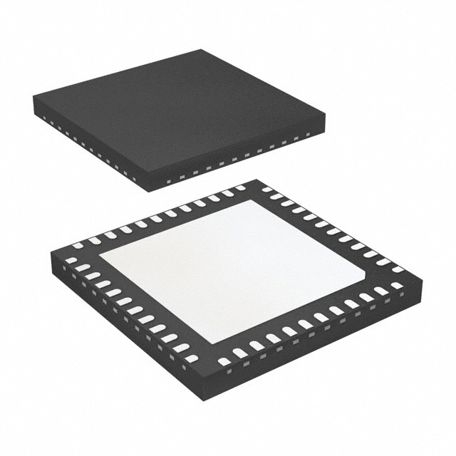


 工商网监
湘ICP备2023018690号
工商网监
湘ICP备2023018690号
