ICS932S421C
Integrated
Circuit
Systems, Inc.
PCIe Gen 2 and QPI Clock for Intel-based Servers
Recommended Application:
PCIe Gen 2 & QPI compliant CK410B+ clock for Intel-based
servers
Key Specifications:
•
PCIe Gen 2 compliant SRC outputs
•
QPI & FBD 2 compliant CPU clocks
•
CPU cycle-cycle jitter: < 50ps
•
SRC cycle-cycle jitter: < 125ps
•
PCI cycle-cycle jitter: < 500ps
•
CPU output skew: < 50ps
•
SRC output skew: < 250ps
•
± 100ppm frequency accuracy on all outputs
Output Features:
•
4 - 0.7V current-mode differential CPU pairs
•
5 - 0.7V current-mode differential SRC pair
•
4 - PCI (33MHz)
•
3 - PCICLK_F, (33MHz) free-running
•
1 - 48MHz
•
2 - REF, 14.318MHz
Functionality
1
FS_C
Features/Benefits:
•
Supports spread spectrum modulation, 0 to -0.5%
down spread
•
Uses external 14.318MHz crystal and external load
capacitors for low ppm synthesis error
•
•
•
CPU clocks independent of SRC/PCI clocks
D2/D3 SMBus address
Increased CPU amplitude at higher speeds compared
to 932S421B
0
0
0
0
1
1
1
1
1
2
FS_B
FS_A
0
0
1
1
0
0
1
1
0
1
0
1
0
1
0
1
CPU
SRC
MHz
MHz
266.67
133.33
200.00
166.67
100.00
333.33
100.00
400.00
Reserved
PCI
MHz
REF
MHz
USB
MHz
33.33
14.32
48.00
1. FS_B and FS_C are three-level inputs. Please see VIL_FS and VIH_FS specifications in
the Input/Supply/Common Output Parameters Table for correct values.
Also refer to the Test Clarification Table.
2. FS_A is a low-threshold input. Please see the VIL_FS and VIH_FS
specifications in the Input/Supply/Common Output Parameters Table for correct values.
VDDPCI
GNDPCI
PCICLK0
PCICLK1
PCICLK2
PCICLK3
GNDPCI
VDDPCI
PCICLK_F0
PCICLK_F1
PCICLK_F2
VDD48
48MHz
GND48
VDDSRC
SRCCLKT0
SRCCLKC0
SRCCLKC1
SRCCLKT1
GNDSRC
SRCCLKT2
SRCCLKC2
SRCCLKC3
SRCCLKT3
VDDSRC
SRCCLKT4
SRCCLKC4
VDDSRC
1460E—08/25/09
1
2
3
4
5
6
7
8
9
10
11
12
13
14
15
16
17
18
19
20
21
22
23
24
25
26
27
28
ICS932S421
Pin Configuration
56
55
54
53
52
51
50
49
48
47
46
45
44
43
42
41
40
39
38
37
36
35
34
33
32
31
30
29
FS_C/TEST_SEL
REF0
REF1
VDDREF
X1
X2
GNDREF
FS_B/TEST_MODE
FS_A
VDDCPU
CPUCLKT0
CPUCLKC0
VDDCPU
CPUCLKT1
CPUCLKC1
GNDCPU
CPUCLKT2
CPUCLKC2
VDDCPU
CPUCLKT3
CPUCLKC3
VDDA
GNDA
IREF
NC
Vtt_PwrGd#/PD
SDATA
SCLK
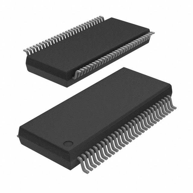
56-pin SSOP & TSSOP
�Integrated
Circuit
Systems, Inc.
ICS932S421C
Pin Description
Pin #
1
2
3
4
5
6
7
8
9
10
11
12
13
14
15
16
17
18
19
20
21
22
23
24
25
26
27
28
PIN NAME
VDDPCI
GNDPCI
PCICLK0
PCICLK1
PCICLK2
PCICLK3
GNDPCI
VDDPCI
PCICLK_F0
PCICLK_F1
PCICLK_F2
VDD48
48MHz
GND48
VDDSRC
SRCCLKT0
SRCCLKC0
SRCCLKC1
SRCCLKT1
GNDSRC
SRCCLKT2
SRCCLKC2
SRCCLKC3
SRCCLKT3
VDDSRC
SRCCLKT4
SRCCLKC4
VDDSRC
PIN TYPE
PWR
PWR
OUT
OUT
OUT
OUT
PWR
PWR
OUT
OUT
OUT
PWR
OUT
PWR
PWR
OUT
OUT
OUT
OUT
PWR
OUT
OUT
OUT
OUT
PWR
OUT
OUT
PWR
DESCRIPTION
Power supply for PCI clocks, nominal 3.3V
Ground pin for the PCI outputs
PCI clock output.
PCI clock output.
PCI clock output.
PCI clock output.
Ground pin for the PCI outputs
Power supply for PCI clocks, nominal 3.3V
Free running PCI clock not affected by PCI_STOP# .
Free running PCI clock not affected by PCI_STOP# .
Free running PCI clock not affected by PCI_STOP# .
Power pin for the 48MHz output.3.3V
48MHz clock output.
Ground pin for the 48MHz outputs
Supply for SRC clocks, 3.3V nominal
True clock of differential SRC clock pair.
Complementary clock of differential SRC clock pair.
Complementary clock of differential push-pull SRC clock pair.
True clock of differential SRC clock pair.
Ground pin for the SRC outputs
True clock of differential SRC clock pair.
Complementary clock of differential SRC clock pair.
Complementary clock of differential SRC clock pair.
True clock of differential SRC clock pair.
Supply for SRC clocks, 3.3V nominal
True clock of differential SRC clock pair.
Complementary clock of differential SRC clock pair.
Supply for SRC clocks, 3.3V nominal
1460E—08/25/09
2
�Integrated
Circuit
Systems, Inc.
ICS932S421C
Pin Description (Continued)
Pin #
29
30
PIN NAME
SCLK
SDATA
Type
IN
I/O
31
Vtt_PwrGd#/PD
IN
32
NC
N/A
33
IREF
OUT
34
35
GNDA
VDDA
PWR
PWR
36
CPUCLKC3
OUT
37
CPUCLKT3
OUT
38
VDDCPU
PWR
39
CPUCLKC2
OUT
40
CPUCLKT2
OUT
41
GNDCPU
PWR
42
CPUCLKC1
OUT
43
CPUCLKT1
OUT
44
VDDCPU
PWR
45
CPUCLKC0
OUT
46
CPUCLKT0
OUT
47
VDDCPU
PWR
48
FS_A
IN
49
FS_B/TEST_MODE
IN
50
51
52
53
54
55
GNDREF
X2
X1
VDDREF
REF1
REF0
56
FS_C/TEST_SEL
PWR
OUT
IN
PWR
OUT
OUT
IN
Pin Description
Clock pin of SMBus circuitry, 5V tolerant.
Data pin for SMBus circuitry, 3.3V tolerant.
Vtt_PwrGd# is an active low input used to determine when latched inputs are ready to
be sampled. PD is an asynchronous active high input pin used to put the device into a
low power state. The internal clocks, PLLs and the crystal oscillator are stopped.
No Connection.
This pin establishes the reference current for the differential current-mode output pairs.
This pin requires a fixed precision resistor tied to ground in order to establish the
appropriate current. 475 ohms is the standard value.
Ground pin for the PLL core.
3.3V power for the PLL core.
Complementary clock of differential pair CPU outputs. These are current mode
outputs. External resistors are required for voltage bias.
True clock of differential pair CPU outputs. These are current mode outputs. External
resistors are required for voltage bias.
Supply for CPU clocks, 3.3V nominal
Complementary clock of differential pair CPU outputs. These are current mode
outputs. External resistors are required for voltage bias.
True clock of differential pair CPU outputs. These are current mode outputs. External
resistors are required for voltage bias.
Ground pin for the CPU outputs
Complementary clock of differential pair CPU outputs. These are current mode
outputs. External resistors are required for voltage bias.
True clock of differential pair CPU outputs. These are current mode outputs. External
resistors are required for voltage bias.
Supply for CPU clocks, 3.3V nominal
Complementary clock of differential pair CPU outputs. These are current mode
outputs. External resistors are required for voltage bias.
True clock of differential pair CPU outputs. These are current mode outputs. External
resistors are required for voltage bias.
Supply for CPU clocks, 3.3V nominal
3.3V tolerant input for CPU frequency selection. Refer to input electrical characteristics
for Vil_FS and Vih_FS values.
3.3V tolerant input for CPU frequency selection. Refer to input electrical characteristics
for Vil_FS and Vih_FS values. TEST_MODE is a real time input to select between Hi-Z
and REF/N divider mode while in test mode. Refer to Test Clarification Table.
Ground pin for the REF outputs.
Crystal output, Nominally 14.318MHz
Crystal input, Nominally 14.318MHz.
Ref, XTAL power supply, nominal 3.3V
14.318 MHz reference clock.
14.318 MHz reference clock.
3.3V tolerant input for CPU frequency selection. Low voltage threshold inputs, see
input electrical characteristics for Vil_FS and Vih_FS values.
TEST_Sel: 3-level latched input to enable test mode.
Refer to Test Clarification Table
1460E—08/25/09
3
�Integrated
Circuit
Systems, Inc.
ICS932S421C
General Description
The ICS932S421C is a main clock synthesizer for CK410B+ generation Intel server platforms. The ICS932S421C is driven
with a 14.318MHz crystal. It generates CPU outputs up to 400MHz and PCI-Express clocks at 100 or 200 MHz. The 48 MHz
USB clock is an exact 48.000 MHz clock.
Block Diagram
REF(1:0)
X1
X2
XTAL
OSC.
48MHz
FIXED PLL
DIVIDER
CPU PLL
DIVIDERS
SRC/PCI
PLL
DIVIDERS
CPUCLK(3:0)
SRCCLK(4:0)
PCICLK(3:0), PCICLK_F(2:0)
FS(C:A)
TEST_SEL
CONTROL
LOGIC
VTT_PWRGD#/PD
SDATA
SCLK
IREF
Power Groups
Pin Number
VDD
GND
53
50
1,8
2,7
15,25,28
20
35
34
12
14
47,44,38
41
Description
Xtal, Ref
PCICLK outputs
SRCCLK outputs
Master clock, CPU Analog
48MHz, PLL_48
CPUCLK clocks
1460E—08/25/09
4
�Integrated
Circuit
Systems, Inc.
ICS932S421C
Single-ended Output Terminations
ICS932S421C
Zo
Rs
CL=5pF
Test Load
SEPP Output Buffer
(Single Ended
Push Pull)
Zo
Rs
CL=5pF
Zo
Rs
CL=5pF
SEPP Output Buffer
(Single Ended
Push Pull)
The singled-ended outputs of the ICS 932S421C default to a drive strength of 2
loads. The REF clocks can be turned down to 1-load strength via the SMBus.
Suggested termination resistors are as follows for transmission lines with Zo =
50 ohms:
Single-ended outputs at 2-load strength (Power up default
for all single-ended outputs)
Driving 1 load, Rs = 33 ohms
Driving 2 loads, Rs = 7.5 ohms
Single-ended outputs at 1-load strength (REF clock only)
Driving 1 load, Rs = 22 ohms
1460E—08/25/09
5
�Integrated
Circuit
Systems, Inc.
ICS932S421C
Absolute Maximum Rating
PARAMETER
SYMBOL
3.3V Core Supply Voltage VDD_A
3.3V Logic Input Supply
VDD_In
Voltage
Storage Temperature
Ts
Ambient Operating Temp Tambient
Case Temperature
Tcase
Input ESD protection HBM ESD prot
CONDITIONS
-
MIN
-
TYP
MAX
VDD + 0.5V
UNITS
V
Notes
1
GND - 0.5
VDD + 0.5V
V
1
-65
0
150
70
115
°
C
°C
°C
V
1
1
1
1
UNITS
V
V
uA
Notes
1
1
1
-5
uA
1
-200
uA
1
2000
1
Guaranteed by design and characterization, not 100% tested in production.
Electrical Characteristics - Input/Supply/Common Output Parameters
PARAMETER
Input High Voltage
Input Low Voltage
Input High Current
SYMBOL
VIH
VIL
I IH
CONDITIONS*
3.3 V +/-5%
3.3 V +/-5%
V IN = VDD
VIN = 0 V; Inputs with no pull-up
resistors
VIN = 0 V; Inputs with pull-up
resistors
MIN
2
VSS - 0.3
-5
VIH_FS
3.3 V +/-5%
0.7
VDD + 0.3
V
1
VSS - 0.3
0.35
V
1
350
70
12
7
5
6
5
mA
mA
mA
MHz
nH
pF
pF
pF
1
1
1
2
1
1
1
1
1.8
ms
1
33
kHz
1
300
us
1
5
5
5.5
0.4
ns
ns
V
V
1
1
1
1
mA
1
1000
ns
1
300
ns
1
IIL1
Input Low Current
IIL2
Low Threshold InputHigh Voltage
Low Threshold InputLow Voltage
Operating Supply Current
VIL_FS
3.3 V +/-5%
IDD3.3OP
Powerdown Current
I DD3.3PD
Input Frequency
Pin Inductance
Fi
Lpin
CIN
COUT
CINX
Full Active, CL = Full load;
all diff pairs driven
all differential pairs tri-stated
VDD = 3.3 V
Input Capacitance
Clk Stabilization
TSTAB
Modulation Frequency
Tdrive_PD
Tfall_PD
Trise_PD
SMBus Voltage
Low-level Output Voltage
Current sinking at
VOL = 0.4 V
SCLK/SDATA
Clock/Data Rise Time
SCLK/SDATA
Clock/Data Fall Time
VDD
VOL
Logic Inputs
Output pin capacitance
X1 & X2 pins
From VDD Power-Up or deassertion of PD to 1st clock
Triangular Modulation
CPU output enable after
PD de-assertion
PD fall time of
PD rise time of
TRI2C
TFI2C
MAX
VDD + 0.3
0.8
5
14.31818
30
2.7
@ IPULLUP
IPULLUP
TYP
4
(Max VIL - 0.15) to
(Min VIH + 0.15)
(Min VIH + 0.15) to
(Max VIL - 0.15)
*TA = 0 - 70°C; Supply Voltage VDD = 3.3 V +/-5%
1
2
Guaranteed by design and characterization, not 100% tested in production.
Input frequency should be measured at the REF pin and tuned to ideal 14.31818MHz to meet ppm frequency accuracy on PLL outputs.
1460E—08/25/09
6
�Integrated
Circuit
Systems, Inc.
ICS932S421C
Electrical Characteristics - CPU 0.7V Current Mode Differential Pair
PARAMETER
Current Source Output
Impedance
Voltage High
Voltage Low
Max Voltage
Min Voltage
Crossing Voltage (abs)
SYMBOL
CONDITIONS*
MIN
Zo
VO = Vx
3000
VHigh
VLow
Vovs
Vuds
Vx(abs)
Statistical measurement on
single ended signal
Measurement on single ended
signal using absolute value.
660
-150
Crossing Voltage (var)
d-Vx
Rise Time
Fall Time
Rise Time Variation
Fall Time Variation
tr
tf
d-tr
d-tf
Duty Cycle
dt3
Skew
tsk3
Jitter, Cycle to cycle
tjcyc-cyc
TYP
UNITS NOTES
Ω
1
550
mV
mV
mV
mV
mV
1,3
1,3
1
1
1
140
mV
1
175
175
525
525
125
125
ps
ps
ps
ps
1
1
1
1
45
55
%
1
50
ps
1
50
ps
1
850
150
1150
-300
250
Variation of crossing over all
edges
VOL = 0.175V, VOH = 0.525V
VOL = 0.175V, VOH = 0.525V
VOL = 0.175V, VOH = 0.525V
VOL = 0.175V, VOH = 0.525V
Measurement from differential
waveform
across all CPU outputs,
VT = 50%
Measurement from differential
waveform
MAX
*TA = 0 - 70°C; VDD = 3.3 V +/-5%; CL =2pF, RS=33.2Ω, RP=49.9Ω, ΙREF = 475Ω
1
Guaranteed by design and characterization, not 100% tested in production.
2
All Long Term Accuracy and Clock Period specifications are guaranteed assuming that REF is at 14.31818MHz
3
IREF = VDD/(3xRR). For RR = 475Ω (1%), IREF = 2.32mA. IOH = 6 x IREF and VOH = 0.7V @ ZO=50Ω.
Electrical Characteristics - SRC 0.7V Current Mode Differential Pair
PARAMETER
Current Source Output
Impedance
Voltage High
Voltage Low
Max Voltage
Min Voltage
Crossing Voltage (abs)
SYMBOL
CONDITIONS*
MIN
Zo
VO = Vx
3000
VHigh
VLow
Vovs
Vuds
Vx(abs)
Statistical measurement on
single ended signal
Measurement on single ended
signal using absolute value.
660
-150
Crossing Voltage (var)
d-Vx
Rise Time
Fall Time
Rise Time Variation
Fall Time Variation
tr
tf
d-tr
d-tf
Duty Cycle
dt3
Skew
tsk3
Jitter, Cycle to cycle
tjcyc-cyc
Variation of crossing over all
edges
VOL = 0.175V, VOH = 0.525V
VOH = 0.525V VOL = 0.175V
VOL = 0.175V, VOH = 0.525V
VOH = 0.525V VOL = 0.175V
Measurement from differential
waveform
VT = 50%
Measurement from differential
waveform
-300
250
7
Ω
1
550
mV
mV
mV
mV
mV
1,3
1,3
1
1
1
850
150
1150
mV
1
ps
ps
ps
ps
1
1
1
1
45
55
%
1
250
ps
1
125
ps
1
All Long Term Accuracy and Clock Period specifications are guaranteed assuming that REF is at 14.31818MHz
1460E—08/25/09
Notes
525
525
125
125
Guaranteed by design and characterization, not 100% tested in production.
IREF = VDD/(3xRR). For RR = 475Ω (1%), IREF = 2.32mA. IOH = 6 x IREF and VOH = 0.7V @ ZO=50Ω.
UNITS
140
*TA = 0 - 70°C; VDD = 3.3 V +/-5%; CL =2pF, RS=33.2Ω, RP=49.9Ω, ΙREF = 475Ω
3
MAX
175
175
1
2
TYP
�Integrated
Circuit
Systems, Inc.
ICS932S421C
Electrical Characteristics - PCICLK/PCICLK_F
PARAMETER
Long Accuracy
Clock period
SYMBOL
ppm
Tperiod
CONDITIONS*
see Tperiod min-max values
33.33MHz output nominal
MIN
-100
29.9970
Absolute Clock period
Tpabs
33.33MHz output including jitter
29.4970
Clock period w/spread
Absolute Clock period
w/spread
Clock High Time
Clock Low Time
Output Impedance
Output High Voltage
Output Low Voltage
TperiodSS
33.33MHz output nominal
30.0722
TpabsSS
33.33MHz output including jitter
THIGH
TLOW
RDSP
VOH
VOL
Output High Current
IOH
1.5V
1.5V
VO = VDD*(0.5)
IOH = -1 mA
IOL = 1 mA
V OH @MIN = 1.0 V
VOH@MAX = 3.135 V
VOL @ MIN = 1.95 V
VOL @ MAX = 0.4 V
Rising/Falling edge rate
VOL = 0.4 V, VOH = 2.4 V
VOH = 2.4 V, VOL = 0.4 V
VT = 1.5 V
VT = 1.5 V
VT = 1.5 V
Output Low Current
IOL
Edge Rate
Rise Time
Fall Time
Duty Cycle
Group Skew
Jitter, Cycle to cycle
tslewr/f
tr
tf
dt1
tskew
tjcyc-cyc
TYP
30
ns
2
30.0852
ns
2, 3
29.5722
30.5852
ns
2,3
12
12
12
2.4
N/A
N/A
55
ns
1
1
1
1
1
1
1
1
1
1
1
1
1
1
1
30.07519
0.55
-33
-33
30
1
0.5
0.5
45
1
Guaranteed by design and characterization, not 100% tested in production.
2
All Long Term Accuracy and Clock Period specifications are guaranteed assuming that REF is at 14.31818MHz
3
Does not apply to 932S431A
8
UNITS NOTES
ppm
1,2
ns
2
30.5030
*TA = 0 - 70°C; Supply Voltage VDD = 3.3 V +/-5% (unless otherwise specified)
1460E—08/25/09
MAX
100
30.0030
38
4
2
2
55
250
500
ns
V
V
mA
mA
mA
mA
V/ns
ns
ns
%
ps
ps
�Integrated
Circuit
Systems, Inc.
ICS932S421C
Electrical Characteristics - USB48MHz
PARAMETER
Long Accuracy
Clock period
SYMBOL
ppm
Tperiod
CONDITIONS*
see Tperiod min-max values
48.00MHz output nominal
MIN
0
20.8333
Absolute Clock period
Tpabs
48.00MHz output including jitter
20.4833
21.1833
Output Impedance
Output High Voltage
Clock High Time
Clock Low Time
Output Low Voltage
RDSP
VOH
THIGH
TLOW
VOL
12
2.4
8.094
7.694
55
Output High Current
IOH
VO = VDD*(0.5)
IOH = -1 mA
1.5V
1.5V
IOL = 1 mA
V OH @MIN = 1.0 V
VOH@MAX = 3.135 V
V OL @ MIN = 1.95 V
V OL @ MAX = 0.4 V
Output Low Current
Edge Rate
Rise Time
Fall Time
Duty Cycle
Group Skew
Jitter, Cycle to cycle
IOL
tslewr/f_USB USB48 Rising/Falling edge rate
tr_USB
tf_USB
dt1
tskew
tjcyc-cyc
VOL = 0.4 V, VOH = 2.4 V
VOH = 2.4 V, V OL = 0.4 V
VT = 1.5 V
VT = 1.5 V
VT = 1.5 V
TYP
20.83333
2
2
27
1
2
V/ns
1
1
1
45
2
2
55
250
350
ns
ns
%
ps
ps
1
1
1
1
1
10.036
9.836
0.55
-29
-33
29
All Long Term Accuracy and Clock Period specifications are guaranteed assuming that REF is at 14.31818MHz
9
ns
ns
V
mA
mA
mA
mA
Guaranteed by design and characterization, not 100% tested in production.
1460E—08/25/09
UNITS NOTES
ppm
1,2
ns
2
1
1
1
1
1
1
1
1
1
*TA = 0 - 70°C; Supply Voltage VDD = 3.3 V +/-5%
1
MAX
0
20.8333
V
ns
�Integrated
Circuit
Systems, Inc.
ICS932S421C
Electrical Characteristics - REF
PARAMETER
Long Accuracy
Clock period
SYMBOL
ppm
Tperiod
Absolute Clock period
Tpabs
Clock High Time
Clock Low Time
Output High Voltage
Output Low Voltage
THIGH
TLOW
VOH
VOL
Output High Current
Output Low Current
Edge Rate
Rise Time
Fall Time
Skew
Duty Cycle
Jitter
CONDITIONS
see Tperiod min-max values
14.318MHz output nominal
14.318MHz output including
jitter
1.5V
1.5V
IOH = -1 mA
IOL = 1 mA
V OH @MIN = 1.0 V
VOH@MAX = 3.135 V
V OL @ MIN = 1.95 V
V OL @ MAX = 0.4 V
Rising/Falling edge rate
VOL = 0.4 V, VOH = 2.4 V
VOH = 2.4 V, V OL = 0.4 V
VT = 1.5 V
VT = 1.5 V
VT = 1.5 V
IOH
IOL
t slewr/f
t r1
t f1
tsk1
dt1
tjcyc-cyc
MIN
-100
69.8343
TYP
0
69.84128
MAX
100
69.8483
UNITS
ppm
ns
Notes
1,2
2
68.8343
70.8483
ns
2
27.533718
27.533718
2.4
N/A
N/A
ns
1
1
1
1
1
1
1
1
1
1
1
1
1
1
0.4
-33
-33
30
38
4
2
2
500
55
1000
1
0.5
0.5
45
ns
V
V
mA
mA
mA
mA
V/ns
ns
ns
ps
%
ps
*TA = 0 - 70°C; Supply Voltage VDD = 3.3 V +/-5%
1
2
Guaranteed by design and characterization, not 100% tested in production.
All Long Term Accuracy and Clock Period specifications are guaranteed assuming that REF is at 14.31818MHz
Electrical Characteristics - Differential Jitter Parameters
PARAMETER
Symbol
tjphasePLL
t jphaseLo
tjphaseHigh
Jitter, Phase
tjphFBD1_3.2
G
Conditions
PCIe Gen 1
PCIe Gen 2
10kHz < f < 1.5MHz
PCIe Gen 2
1.5MHz < f < Nyquist (50MHz)
FBD1 3.2/4G
11MHz to 33MHz
tjphFBD1_4.0
G
tjphQPI
FBD1 4.8G
11MHz to 33MHz
QPI 133MHz 6.4GB_12UI
CPU outputs only
*TA = 0 - 70°C; Supply Voltage VDD = 3.3 V +/-5%
1
2
Guaranteed by design and characterization, not 100% tested in production.
See http://www.pcisig.com for complete specs
1460E—08/25/09
10
Min
TYP
40
Max
86
1.7
3
2.2
3.1
2.5
3
2
2.5
0.25
0.5
Units
ps (p-p)
ps
(RMS)
ps
(RMS)
ps
(RMS)
ps
(RMS)
ps
(RMS)
Notes
1,2
1,2
1,2
1,2
1,2
1,2
�Integrated
Circuit
Systems, Inc.
ICS932S421C
Differential Clock AC Tolerances
PPM tolerance
Cycle to Cycle Jitter
Spread
CPU
100
50
-0.50%
SRC
100
125
-0.50%
DOT96
100
250
0
BMC133
100
125
-0.50%
ppm
ps
%
Clock Periods - Differential Outputs with Spread Spectrum Disabled
SSC ON
CPU
SRC
Center
Freq.
MHz
100.00
133.33
166.67
200.00
266.67
333.33
400.00
100.00
Measurement Window
1us
0.1s
0.1s
0.1s
+ ppm
-SSC
- ppm
0 ppm
-c2c jitter
Long-Term
Short-Term Long-Term
Period
AbsPer
Average
Average
Average
Nominal
Min
Max
Min
Min
9.94900
9.99900
10.00000
10.00100
7.44925
7.49925
7.50000
7.50075
5.94940
5.99940
6.00000
6.00060
4.94950
4.99950
5.00000
5.00050
3.69962
3.74962
3.75000
3.75037
2.94970
2.99970
3.00000
3.00030
2.44975
2.49975
2.50000
2.50025
9.87400
9.99900
10.00000
10.00100
1 Clock
1us
+SSC
Short-Term
Average
Max
1 Clock
+c2c jitter Units Notes
AbsPer
Max
10.05100
7.55075
6.05060
5.05050
3.80037
3.05030
2.55025
10.12600
ns
ns
ns
ns
ns
ns
ns
ns
1,2
1,2
1,2
1,2
1,2
1,2
1,2
1,2
Clock Periods - Differential Outputs with Spread Spectrum Enabled
SSC ON
CPU
SRC
1
2
Center
Freq.
MHz
99.75
133.00
166.25
199.50
266.00
332.50
399.00
99.75
Measurement Window
1us
0.1s
0.1s
0.1s
+ ppm
- ppm
-SSC
0 ppm
-c2c jitter
Long-Term
Short-Term Long-Term
Period
AbsPer
Average
Average
Average
Nominal
Min
Max
Min
Min
9.94906
9.99906
10.02406
10.02506
10.02607
7.44930
7.49930
7.51805
7.51880
7.51955
5.94944
5.99944
6.01444
6.01504
6.01564
4.94953
4.99953
5.01203
5.01253
5.01303
3.69965
3.74965
3.75902
3.75940
3.75977
2.94972
2.99972
3.00722
3.00752
3.00782
2.44977
2.49977
2.50602
2.50627
2.50652
9.87406
9.99906
10.02406
10.02506
10.02607
1 Clock
1us
+SSC
Short-Term
Average
Max
10.05107
7.53830
6.03064
5.02553
3.76915
3.01532
2.51277
10.05107
1 Clock
+c2c jitter Units Notes
AbsPer
Max
10.10107
7.58830
6.08064
5.07553
3.81915
3.06532
2.56277
10.17607
ns
ns
ns
ns
ns
ns
ns
ns
1,2
1,2
1,2
1,2
1,2
1,2
1,2
1,2
Guaranteed by design and characterization, not 100% tested in production.
All Long Term Accuracy specifications are guaranteed with the assumption that the crystal input is tuned to exactly 14.31818MHz.
1460E—08/25/09
11
�Integrated
Circuit
Systems, Inc.
ICS932S421C
General SMBus serial interface information for the ICS932S421C
How to Write:
How to Read:
Controller (host) sends a start bit.
Controller (host) sends the write address D2 (H)
ICS clock will acknowledge
Controller (host) sends the beginning byte location = N
ICS clock will acknowledge
Controller (host) sends the data byte count = X
ICS clock will acknowledge
Controller (host) starts sending Byte N through
Byte N + X -1
• ICS clock will acknowledge each byte one at a time
• Controller (host) sends a Stop bit
•
•
•
•
•
•
•
•
•
•
•
•
•
•
•
•
•
•
•
•
•
•
Controller (host) will send start bit.
Controller (host) sends the write address D2 (H)
ICS clock will acknowledge
Controller (host) sends the begining byte
location = N
ICS clock will acknowledge
Controller (host) will send a separate start bit.
Controller (host) sends the read address D3 (H)
ICS clock will acknowledge
ICS clock will send the data byte count = X
ICS clock sends Byte N + X -1
ICS clock sends Byte 0 through byte X (if X(H)
was written to byte 8).
Controller (host) will need to acknowledge each byte
Controller (host) will send a not acknowledge bit
Controller (host) will send a stop bit
Index Block Read Operation
Index Block Write Operation
Controller (Host)
starT bit
T
Slave Address D2(H)
WR
WRite
Controller (Host)
T
starT bit
Slave Address D2(H)
WR
WRite
ICS (Slave/Receiver)
ICS (Slave/Receiver)
ACK
ACK
Beginning Byte = N
Beginning Byte = N
ACK
ACK
RT
Repeat starT
Slave Address D3(H)
RD
ReaD
Data Byte Count = X
ACK
Beginning Byte N
ACK
X Byte
ACK
Data Byte Count = X
ACK
Beginning Byte N
Byte N + X - 1
ACK
X Byte
ACK
P
stoP bit
Byte N + X - 1
N
P
1460E—08/25/09
12
Not acknowledge
stoP bit
�Integrated
Circuit
Systems, Inc.
ICS932S421C
SMBus Table: Output Enable Register
Byte 0
Bit 7
Pin #
NA
Name
SRCCLK7 Enable
Control Function
Output Enable
Type
RW
0
Disable-Hi-Z
1
Enable
PWD
1
Bit 6
NA
SRCCLK6 Enable
Output Enable
RW
Disable-Hi-Z
Enable
1
Bit 5
NA
SRCCLK5 Enable
Output Enable
RW
Disable-Hi-Z
Enable
1
Bit 4
26,27
SRCCLK4 Enable
Output Enable
RW
Disable-Hi-Z
Enable
1
Bit 3
23,24
SRCCLK3 Enable
Output Enable
RW
Disable-Hi-Z
Enable
1
Bit 2
21,22
SRCCLK2 Enable
Output Enable
RW
Disable-Hi-Z
Enable
1
Bit 1
18,19
SRCCLK1 Enable
Output Enable
RW
Disable-Hi-Z
Enable
1
Bit 0
16,17
SRCCLK0 Enable
Output Enable
RW
Disable-Hi-Z
Enable
1
Control Function
Output Enable
Type
RW
0
Disable-Low
1
Enable
PWD
1
REF0 Enable
Output Enable
RW
Disable-Low
Enable
1
Output Enable
RW
Disable-Hi-Z
Enable
1
RW
Disable-Hi-Z
Enable
1
RW
Disable-Hi-Z
Enable
1
SMBus Table: Output Enable Register
Byte 1
Bit 7
Pin #
54
55
Bit 6
Name
REF1 Enable
Bit 5
36,37
CPUCLK3
Bit 4
39,40
CPUCLK2
Output Enable
CPUCLK1
Output Enable
Bit 1
42,43
45,46
CPUCLK0
Output Enable
RW
Disable-Hi-Z
Enable
1
Bit 0
CPU, SRC, PCI
Spread Spectrum Enable
Spread Off/On
RW
Spread Off
Spread On
0
RESERVED
Bit 3
Bit 2
0
SMBus Table: Output Enable Register
Byte 2
Bit 7
Pin #
6
Name
PCICLK3
Control Function
Output Enable
Type
RW
0
Disable-Low
1
Enable
PWD
1
Bit 6
5
PCICLK2
Output Enable
RW
Disable-Low
Enable
1
Bit 5
4
PCICLK1
Output Enable
RW
Disable-Low
Enable
1
Bit 4
3
PCICLK0
Output Enable
RW
Disable-Low
Enable
1
Bit 3
11
PCICLK_F2 Enable
Output Enable
RW
Disable-Low
Enable
1
Bit 2
10
PCICLK_F1 Enable
Output Enable
RW
Disable-Low
Enable
1
Bit 1
9
PCICLK_F0 Enable
Output Enable
RW
Disable-Low
Enable
1
Bit 0
13
48MHz Enable
Output Enable
RW
Disable-Low
Enable
1
Control Function
Type
RW
0
Free-Running
1
Stoppable
PWD
1
SMBus Table: Stop Control Register
Byte 3
Bit 7
Pin #
11
Name
PCICLK_F2 Stop En
Bit 6
10
PCICLK_F1 Stop En
RW
Free-Running
Stoppable
1
Bit 5
9
PCICLK_F0 Stop En
RW
Free-Running
Stoppable
1
Bit 4
26,27
SRCCLK4 Stop En
RW
Free-Running
Stoppable
1
Bit 3
23,24
SRCCLK3 Stop En
RW
Free-Running
Stoppable
1
Bit 2
21,22
SRCCLK2 Stop En
RW
Free-Running
Stoppable
1
Bit 1
18,19
SRCCLK1 Stop En
RW
Free-Running
Stoppable
1
Bit 0
16,17
SRCCLK0 Stop En
RW
Free-Running
Stoppable
1
Free-Running Control,
Default: not affected by
PCI/SRC_STOP
(Byte 6, bit 3)
1460E—08/25/09
13
�Integrated
Circuit
Systems, Inc.
ICS932S421C
SMBus Table: Stop and Power Down Mode Drive Control Register
Byte 4
36,37
Name
CPUCLK3 PD Drive
Control Function
Drive Mode in PD
Type
RW
0
Driven
1
Hi-Z
PWD
0
39,40
CPUCLK2 PD Drive
Drive Mode in PD
RW
Driven
Hi-Z
0
42,43
45,46
CPUCLK1 PD Drive
Drive mode in PD
RW
Driven
Hi-Z
0
Bit 4
CPUCLK0 PD Drive
Drive mode in PD
RW
Driven
Hi-Z
0
Bit 3
36,37
CPUCLK3 Stop En
RW
Free-Running
Stoppable
1
Bit 2
39,40
CPUCLK2 Stop En
RW
Free-Running
Stoppable
1
42,43
45,46
CPUCLK1 Stop En
RW
Free-Running
Stoppable
1
RW
Free-Running
Stoppable
1
Bit 7
Bit 6
Bit 5
Bit 1
Bit 0
Pin #
Free-Running Control,
Default: not affected by
CPU_STOP
CPUCLK0 Stop En
SMBus Table: Stop and Power Down Mode Drive Control Register
Byte 5
Pin #
Name
Control Function
RESERVED
Type
0
1
PWD
0
SRC
SRC Stop Drive Mode
Driven in STOP
RW
Driven
Hi-Z
0
SRC
SRC PD Drive Mode
Driven in PD
RW
Driven
Hi-Z
0
Bit 7
Bit 6
Bit 5
RESERVED
Bit 4
0
Bit 3
36,37
CPUCLK3 Stop Drive
Drive Mode in Stop
RW
Driven
Hi-Z
0
Bit 2
39,40
CPUCLK2 Stop Drive
Drive Mode in Stop
RW
Driven
Hi-Z
0
Bit 1
42,43
45,46
CPUCLK1 Stop Drive
Drive Mode in Stop
RW
Driven
Hi-Z
0
CPUCLK0 Stop Drive
Drive Mode in Stop
RW
Driven
Hi-Z
0
Bit 0
SMBus Table: Test Mode and FS Readback Register
Byte 6
Bit 7
-
Pin #
Name
Test Mode Selection
Control Function
Test Mode Selection
Type
RW
0
Hi-Z
1
REF/N
PWD
0
Bit 6
-
Test Clock Mode Entry
Test Mode
RW
Disable
Enable
0
Bit 5
-
RW
1X
2X
1
RW
Stop
Run
1
RESERVED
0
Bit 4
54,55
REF Drive Strength
Bit 3
PCI, SRC
PCI_STOP Control
Bit 2
-
FS_C
1X or 2X
Stop non-free running PC
and SRC clocks.
FS_C readback
-
FS_B
FS_B readback
R
FS_A
FS_A readback
R
Control Function
Bit 1
Bit 0
R
See 932S421 Functionality
Table
Latch
Latch
Latch
SMBus Table: Vendor & Revision ID Register
Byte 7
Type
0
1
PWD
Bit 7
-
Pin #
Name
RID3
R
-
-
0
Bit 6
-
RID2
R
-
-
0
Bit 5
-
RID1
R
-
-
1
Bit 4
-
RID0
R
-
-
0
Bit 3
-
VID3
R
-
-
0
Bit 2
-
VID2
Bit 1
-
VID1
Bit 0
-
VID0
REVISION ID
VENDOR ID
1460E—08/25/09
14
R
-
-
0
R
-
-
0
R
-
-
1
�Integrated
Circuit
Systems, Inc.
ICS932S421C
SMBus Table: Byte Count Register
Byte 8
Bit 7
-
Pin #
Name
BC7
Control Function
Bit 6
-
BC6
RW
Bit 5
-
BC5
RW
Bit 4
-
BC4
Bit 3
-
BC3
Bit 2
-
BC2
RW
Bit 1
-
BC1
RW
1
Bit 0
-
BC0
RW
1
Byte Count Programming
b(7:0)
Type
RW
RW
RW
0
1
PWD
0
0
Writing to this register will
configure how many bytes will
be read back, default is 8
bytes.
(0 to 7)
0
0
0
1
SMBus Table: Device ID Register
Byte 9
Bit 7
Pin #
Name
DID7
Bit 6
Bit 5
Bit 4
DID4
Bit 3
DID3
Control Function
Type
R
0
-
1
-
PWD
0
DID6
R
-
-
0
DID5
R
-
-
1
R
-
-
0
R
-
-
1
Bit 2
DID2
R
-
-
0
Bit 1
DID1
R
-
-
1
Bit 0
DID0
R
-
-
1
0
1
PWD
Disable
Enable
0
Stop
Run
1
Device ID
(2B hex)
SMBus Table: M/N Programming & Control Register
Byte 10
Pin #
Name
Bit 7
-
M/N_EN
Bit 6
CPU
CPU_STOP Control
Bit 5
-
Bit 4
-
Bit 3
SRC, PCI
SRC Alternate Frequency (96% of
Nominal)
Bit 2
CPU
Bit 1
54
CPU Alternate Frequency (96% of
Nominal) Only active if latched
frequency is 166 MHz or 333
MHz.
REF1 Drive Strength
55
REF0 Drive Strength
Bit 0
Control Function
Type
CPU and SRC
M/N Programming
RW
Enable
Stop non-free running PC
RW
and SRC clocks.
RESERVED
RESERVED
Set SRC = 96 MHz and
PCI = 32 MHz
Only active if
Byte 10, bit 2 = 1
Set alternate CPU
frequency:
166 MHz to 160 MHz
333 MHz to 320 MHz
1X or 2X
1X or 2X
RW
1460E—08/25/09
15
0
0
RW
Normal
Alternate
Frequency
0
RW
Normal
Alternate
Frequency
0
RW
See REF Drive Strength
Functionality Table
1
1
�Integrated
Circuit
Systems, Inc.
ICS932S421C
SMBus Table: CPU Frequency Control Register
Byte 11
Bit 7
-
Pin #
Name
CPU N Div8
Control Function
N Divider Prog bit 8
Type
RW
Bit 6
-
CPU N Div9
N Divider Prog bit 9
RW
Bit 5
-
CPU M Div5
RW
Bit 4
-
CPU M Div4
RW
Bit 3
-
CPU M Div3
Bit 2
-
CPU M Div2
Bit 1
-
CPU M Div1
RW
Bit 0
-
CPU M Div0
RW
M Divider Programming
bit (5:0)
RW
RW
0
1
The decimal representation of
M and N Divider in Byte 11 and
12 will configure the CPU VCO
frequency. Default at power up
= latch-in or Byte 0 Rom table.
VCO Frequency = 14.318 x
[NDiv(9:0)+8] / [MDiv(5:0)+2]
PWD
X
X
X
X
X
X
X
X
SMBus Table: CPU Frequency Control Register
Byte 12
Bit 7
-
Pin #
Name
CPU N Div7
Control Function
Bit 6
-
CPU N Div6
RW
Bit 5
-
CPU N Div5
RW
Bit 4
-
CPU N Div4
Bit 3
-
CPU N Div3
Bit 2
-
CPU N Div2
RW
Bit 1
-
CPU N Div1
RW
Bit 0
-
CPU N Div0
RW
N Divider Programming
Byte12 bit(7:0) and
Byte11 bit(7:6)
Type
RW
RW
RW
0
1
The decimal representation of
M and N Divider in Byte 11 and
12 will configure the CPU VCO
frequency. Default at power up
= latch-in or Byte 0 Rom table.
VCO Frequency = 14.318 x
[NDiv(9:0)+8] / [MDiv(5:0)+2]
PWD
X
X
X
X
X
X
X
X
SMBus Table: CPU Spread Spectrum Control Register
Byte 13
Pin #
Name
Control Function
Type
0
1
PWD
Bit 7
-
CPU SSP7
RW
X
Bit 6
-
CPU SSP6
RW
X
Bit 5
-
CPU SSP5
RW
Bit 4
-
CPU SSP4
Bit 3
-
CPU SSP3
Bit 2
-
CPU SSP2
RW
X
Bit 1
-
CPU SSP1
RW
X
Bit 0
-
CPU SSP0
RW
X
Spread Spectrum
Programming bit(7:0)
RW
RW
X
These Spread Spectrum bits in
Byte 13 and 14 will program the
spread pecentage of CPU
X
X
SMBus Table: CPU Spread Spectrum Control Register
Byte 14
Pin #
Name
Control Function
Reserved
Type
0
1
PWD
0
Bit 7
-
Bit 6
-
CPU SSP14
RW
Bit 5
-
CPU SSP13
RW
Bit 4
-
CPU SSP12
RW
Bit 3
-
CPU SSP11
Bit 2
-
CPU SSP10
Bit 1
-
CPU SSP9
RW
X
Bit 0
-
CPU SSP8
RW
X
Spread Spectrum
Programming bit(14:8)
1460E—08/25/09
16
RW
RW
X
X
These Spread Spectrum bits in
Byte 13 and 14 will program the
spread pecentage of CPU
X
X
X
�Integrated
Circuit
Systems, Inc.
ICS932S421C
SMBus Table: SRC/PCI Frequency Control Register
Byte 15
Bit 7
-
Pin #
Name
SRC N Div8
Control Function
N Divider Prog bit 8
Type
RW
Bit 6
-
SRC N Div9
N Divider Prog bit 9
RW
Bit 5
-
SRC M Div5
RW
Bit 4
-
SRC M Div4
RW
Bit 3
-
SRC M Div3
Bit 2
-
SRC M Div2
Bit 1
-
SRC M Div1
RW
Bit 0
-
SRC M Div0
RW
M Divider Programming
bits
RW
RW
0
1
The decimal representation of
M and N Divider in Byte 15 and
16 will configure the SRC VCO
frequency. Default at power up
= latch-in or Byte 0 Rom table.
VCO Frequency = 14.318 x
[NDiv(9:0)+8] / [MDiv(5:0)+2]
PWD
X
X
X
X
X
X
X
X
SMBus Table: SRC/PCI Frequency Control Register
Byte 16
Bit 7
-
Pin #
Name
SRC N Div7
Control Function
Bit 6
-
SRC N Div6
RW
Bit 5
-
SRC N Div5
RW
Bit 4
-
SRC N Div4
RW
Bit 3
-
SRC N Div3
Bit 2
-
SRC N Div2
RW
Bit 1
-
SRC N Div1
RW
Bit 0
-
SRC N Div0
RW
N Divider Programming
b(7:0)
Type
RW
RW
0
1
The decimal representation of
M and N Divider in Byte 15 and
16 will configure the SRC VCO
frequency. Default at power up
= latch-in or Byte 0 Rom table.
VCO Frequency = 14.318 x
[NDiv(9:0)+8] / [MDiv(5:0)+2]
PWD
X
X
X
X
X
X
X
X
SMBus Table: SRC/PCI Spread Spectrum Control Register
Byte 17
Bit 7
-
Pin #
Name
SRC SSP7
Control Function
Bit 6
-
SRC SSP6
RW
Bit 5
-
SRC SSP5
RW
Bit 4
-
SRC SSP4
Bit 3
-
SRC SSP3
Bit 2
-
SRC SSP2
RW
X
Bit 1
-
SRC SSP1
RW
X
Bit 0
-
SRC SSP0
RW
X
Spread Spectrum
Programming b(7:0)
Type
RW
RW
RW
0
1
PWD
X
X
X
These Spread Spectrum bits in
Byte 17 and 18 will program the
spread pecentage of SRC
X
X
SMBus Table: SRC/PCI Spread Spectrum Control Register
Byte 18
-
Name
Reserved
Bit 6
-
SRC SSP14
RW
X
Bit 5
-
SRC SSP13
RW
X
Bit 4
-
SRC SSP12
Bit 3
-
SRC SSP11
Bit 2
-
SRC SSP10
Bit 1
-
SRC SSP9
RW
X
Bit 0
-
SRC SSP8
RW
X
Bit 7
Pin #
Control Function
Reserved
Spread Spectrum
Programming b(14:8)
1460E—08/25/09
17
Type
R
RW
RW
RW
0
-
1
-
These Spread Spectrum bits in
Byte 17 and 18 will program the
spread pecentage of SRC
PWD
0
X
X
X
�Integrated
Circuit
Systems, Inc.
ICS932S421C
SMBus Table: CPU Programmable Output Divider Register
Byte 19
Pin #
Name
Control Function
Bit 7
-
CPUDiv3
Bit 6
-
CPUDiv2
Bit 5
-
CPUDiv1
Bit 4
-
CPUDiv0
Type
0
1
RW
CPU Divider Ratio
Programming Bits
RW
RW
PWD
X
See CPU, SRC and PCI
Divider Ratios Table
RW
X
X
X
Bit 3
RESERVED
X
Bit 2
RESERVED
X
Bit 1
RESERVED
X
Bit 0
RESERVED
X
SMBus Table: SRC and PCI Programmable Output Divider Register
Byte 20
-
Name
PCIDiv3
Control Function
Bit 7
Pin #
Type
RW
Bit 6
-
PCIDiv2
RW
Bit 5
-
PCIDiv1
PCI Divider Ratio
Programming Bits
Bit 4
-
PCIDiv0
RW
X
Bit 3
-
SRC_Div3
RW
X
Bit 2
-
SRC_Div2
RW
Bit 1
-
SRC_Div1
Bit 0
-
SRC_Div0
SRC_ Divider Ratio
Programming Bits
RW
RW
0
1
See CPU, SRC and PCI
Divider Ratios Table
See CPU, SRC and PCI
Divider Ratios Table
RW
PWD
X
X
X
X
X
X
SMBusTable: Test Byte Register
Byte 21
Type
RW
Test Result
ICS ONLY TEST
Reserved
PWD
0
Bit 6
ICS ONLY TEST
RW
Reserved
0
Bit 5
ICS ONLY TEST
RW
Reserved
0
Bit 4
ICS ONLY TEST
RW
Reserved
0
Bit 3
ICS ONLY TEST
RW
Reserved
0
Bit 2
ICS ONLY TEST
RW
Reserved
0
Bit 1
ICS ONLY TEST
RW
Reserved
0
Bit 0
ICS ONLY TEST
RW
Reserved
0
Bit 7
Test
`
Test Function
Note: Do NOT write to Byte 21. Erratic device operation will result!
1460E—08/25/09
18
�Integrated
Circuit
Systems, Inc.
ICS932S421C
PD, Power Down
PD is an asynchronous active high input used to shut off all clocks cleanly prior to system power down.
When PD is asserted, all clocks will be driven low before turning off the VCO. All clocks will start without glitches when PD is
de-asserted.
PD
CPU
CPU #
SRC
SRC#
PCIF/PCI
USB
REF
Note
0
Normal
Normal
Normal
Normal
33MHz
48MHz
14.318MHz
1
1
Iref * 2 or
Float
Float
Iref * 2
or Float
Float
Low
Low
Low
1
Notes:
1. Refer to SMBus Byte 4 for additional information.
PD Assertion
PD should be sampled high by 2 consecutive CPU# rising edges before stopping clocks. All single ended clocks will be held
low on their next high to low transition.
All differential clocks will be held high on the next high to low transition of the complimentary clock. If the control register
determining to drive mode is set to 'tri-state', the differential pair will be stopped in tri-state mode, undriven.
When the drive mode corresponding to the CPU or SRC clock of interest is set to '0' the true clock will be driven high at 2 x
Iref and the complementary clock will be tristated. If the control register is programmed to '1' both clocks will be tristated.
See SMBus Bytes 4 and 5 for additional information.
PD
CPU, 133MHz
CPU#, 133MHz
SRC, 100MHz
SRC#, 100MHz
USB, 48MHz
PCI, 33MHz
REF, 14.31818
CPU, SRC and PCI Divider Ratios
Div(3:0)
Divider
0
0000
2
1
0001
3
2
0010
5
3
0011
15
4
0100
4
5
0101
6
6
0110
10
7
0111
30
8
1000
8
9
1001
12
10
1010
20
11
1011
60
12
1100
16
13
1101
24
14
1110
40
15
1111
120
REF Drive Strength Functionality
Byte6,
Byte Byte 10,
bit 4 10, bit 1 bit 0
0
X
X
1
0
0
1
0
1
1
1
0
1
1
1
1460E—08/25/09
19
REF1
1x
1x
1x
2x
2x
REF0
1x
1x
2x
1x
2x
�Integrated
Circuit
Systems, Inc.
ICS932S421C
PD De-assertion
The time from the de-assertion of PD or until power supply ramps to get stable clocks will be less than 1.8ms. If the drive
mode control bit for PD tristate is programmed to '1' the stopped differential pair must first be driven high to a minimum of
200mV in less than 300µs of PD deassertion.
Tstable
3-level latched input
If power-up w/ V>2.0V (-0.3V) then use TEST_SEL
If power-up w/ Vlow Vth input
TEST_MODE is a real time input
SW
TEST
FS_C/TEST FS_B/TEST ENTRY
BIT
_SEL
_MODE
B6b6
HW PIN HW PIN
0
X
0
1
0
X
1
0
X
1
1
X
If TEST_SEL HW pin is 0 during power-up,
test mode can be invoked through B6b6.
If test mode is invoked by B6b6, only B6b7
is used to select HI-Z or REF/N
FS_B/TEST_Mode pin is not used.
Cycle power to disable test mode, one shot control
1
1
X
1
REF/N
0
X
1
0
HI-Z
0
X
1
1
REF/N
B6b6: 1= ENTER TEST MODE, Default = 0 (NORMAL OPERATION)
B6b7: 1= REF/N, Default = 0 (HI-Z)
1460E—08/25/09
20
REF/N or
HI-Z
B6b7
OUTPUT
X
NORMAL
0
HI-Z
1
REF/N
0
REF/N
�Integrated
Circuit
Systems, Inc.
ICS932S421C
c
N
SYMBOL
A
A1
b
c
D
E
E1
e
h
L
N
a
L
E1
INDEX
AREA
E
1 2
α
h x 45°
D
In Millimeters
COMMON DIMENSIONS
MIN
MAX
2.41
2.80
0.20
0.40
0.20
0.34
0.13
0.25
SEE VARIATIONS
10.03
10.68
7.40
7.60
0.635 BASIC
0.38
0.64
0.50
1.02
SEE VARIATIONS
0°
8°
In Inches
COMMON DIMENSIONS
MIN
MAX
.095
.110
.008
.016
.008
.0135
.005
.010
SEE VARIATIONS
.395
.420
.291
.299
0.025 BASIC
.015
.025
.020
.040
SEE VARIATIONS
0°
8°
VARIATIONS
N
A
56
-Cb
D (inch)
MAX
18.55
Reference Doc.: JEDEC Publication 95, MO-118
A1
e
D mm.
MIN
18.31
10-0034
SEATING
PLANE
.10 (.004) C
1460E—08/25/09
21
MIN
.720
MAX
.730
�Integrated
Circuit
Systems, Inc.
ICS932S421C
c
N
L
E1
INDEX
AREA
E
1 2
a
D
A
A2
6.10 mm. Body, 0.50 mm. Pitch TSSOP
(240 mil)
(20 mil)
In Millimeters
In Inches
SYMBOL COMMON DIMENSIONS COMMON DIMENSIONS
MIN
MAX
MIN
MAX
A
-1.20
-.047
A1
0.05
0.15
.002
.006
A2
0.80
1.05
.032
.041
b
0.17
0.27
.007
.011
c
0.09
0.20
.0035
.008
SEE VARIATIONS
SEE VARIATIONS
D
8.10 BASIC
0.319 BASIC
E
E1
6.00
6.20
.236
.244
0.50 BASIC
0.020 BASIC
e
L
0.45
0.75
.018
.030
SEE VARIATIONS
SEE VARIATIONS
N
α
0°
8°
0°
8°
aaa
-0.10
-.004
VARIATIONS
N
A1
56
-C-
D mm.
MIN
13.90
D (inch)
MAX
14.10
Reference Doc.: JEDEC Publication 95, MO-153
e
SEATING
PLANE
b
10-0039
aaa C
Ordering Information
Part / Order Number
932S421CFLF
932S421CFLFT
932S421CGLF
932S421CGLFT
Shipping Packaging
Tubes
Tape and Reel
Tubes
Tape and Reel
Package
56-pin SSOP
56-pin SSOP
56-pin TSSOP
56-pin TSSOP
Temperature
0 to +70° C
0 to +70° C
0 to +70° C
0 to +70° C
“LF” after the package code denotes Pb-Free configuration, RoHS compliant.
1460E—08/25/09
22
MIN
.547
MAX
.555
�Integrated
Circuit
Systems, Inc.
ICS932S421C
Revision History
Rev.
A
B
C
D
E
Issue Date
4/15/2008
9/17/2008
11/20/2008
Description
Initial Release
Updated electrical characteristics, PPM and clock period data
Added 48MHz electrical char table.
Corrected Byte 10 bits 4 and 5 to reserved. For non-spread PCIe
6/9/2009 applications see the 932S431.
1. Updated Byte 3 table.
8/25/2009
2. Added new ordering info table.
1460E—08/25/09
23
Page #
Various
9
15
Various
�


 工商网监
湘ICP备2023018690号
工商网监
湘ICP备2023018690号
