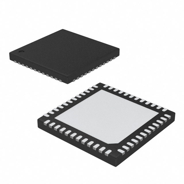
9-Output 3.3V PCIe Fanout Buffer
9DBL09x1
DATASHEET
Description
Features/Benefits
The 9DBL09x1 devices are 3.3V members of IDT's
Full-Featured PCIe clock family. The 9DBL09x1 devices
support PCIe Gen1–4 Common Clocked (CC) and PCIe
Separate Reference Independent Spread (SRIS) systems.
They offer a choice of integrated output terminations
providing direct connection to 85Ω or 100Ω transmission
lines. The 9DBL09P1 can be factory programmed with a
user-defined power up default SMBus configuration.
• Direct connection to 100 (xx41) or 85 (xx51)
•
•
•
Recommended Application
PCIe Gen1–4 clock distribution for Riser Cards, Storage,
Networking, JBOD, Communications, Access Points
Output Features
• 9 – 1-200 MHz Low-Power (LP) HCSL DIF pairs
•
•
• 9DBL0941 default Zout = 100Ω
• 9DBL0951 default Zout = 85Ω
• 9DBL09P1 factory programmable defaults
Easy AC-coupling to other logic families, see IDT
application note AN-891.
•
•
Key Specifications
•
•
• DIF additive cycle-to-cycle jitter < 5ps
• DIF output-to-output skew < 50ps
• Additive phase jitter is 0ps (typical rms) for PCIe Gen1–4
•
•
CC, SRIS
Additive phase jitter 111fs rms typical at 156.25M (1.5M to
10M)
•
transmission lines; saves 36 resistors compared to
standard PCIe devices
165mW typical power consumption (at 3.3V); eliminates
thermal concerns
VDDIO allows 50% power savings at optional 1.05V;
maximum power savings
SMBus-selectable features allows optimization to customer
requirements:
– control input polarity
– control input pull up/downs
– slew rate for each output
– differential output amplitude
– output impedance for each output
Customer defined SMBus power up default can be
programmed into P1 device; allows exact optimization to
customer requirements
OE# pins; support DIF power management
HCSL differential input; can be driven by common clock
sources
Spread spectrum tolerant; allows reduction of EMI
Device contains default configuration; SMBus interface not
required for device operation
Three selectable SMBus addresses; multiple devices can
easily share an SMBus segment
Space saving 48-pin 6 x 6mm VFQFPN; minimal board
space
Block Diagram
vOE(8 :0)#
9
DIF8
DIF7
DIF6
DIF5
CLK_IN#
DIF4
vSADR
DIF3
^CKPW RGD_P D#
SDA TA_ 3. 3
Control
Logic
CLK_IN
DIF2
DIF1
SCLK_3.3
DIF0
Note: Resistors default to internal on 41/51 devices. P1 devices have programmable default impedances on an output-by-output basis.
9DBL09x1 AUGUST 1, 2017
1
©2017 Integrated Device Technology, Inc.
�9DBL09x1 DATASHEET
vOE5#
VDD3.3
VDDIO
GND
DIF6
DIF6#
vOE6#
DIF7
DIF7#
vOE7#
VDDIO
^CKPWRGD_PD#
Pin Configuration
48 47 46 45 44 43 42 41 40 39 38 37
vSADR_tri 1
36 DIF5#
vOE8# 2
35 DIF5
DIF8 3
34 vOE4#
DIF8# 4
33 DIF4#
VDDR3.3 5
32 DIF4
CLK_IN 6
9DBL09x1
CLK_IN# 7
epad is GND
31 VDDIO
30 VDD3.3
GNDR 8
29 GNDA
GNDDIG 9
28 vOE3#
SCLK_3.3 10
27 DIF3#
SDATA_3.3 11
26 DIF3
VDDDIG3.3 12
25 vOE2#
DIF2#
DIF2
GND
VDDIO
VDD3.3
DIF1#
DIF1
vOE1#
DIF0#
DIF0
vOE0#
VDDIO
13 14 15 16 17 18 19 20 21 22 23 24
48-pin VFQFPN, 6x6 mm, 0.4mm pitch
^v prefix indicates internal 120KOhm pull up AND pull down resistor
(biased to VDD/2)
v prefix indicates internal 120KOhm pull down resistor
^ prefix indicates internal 120KOhm pull up resistor
SMBus Address Selection Table
SADR
0
M
1
State of SADR on first
application of
CKPWRGD_PD#
Address
1101011
1101100
1101101
+
Read/Write bit
x
x
x
Note: If not using CKPWRGD (i.e., CKPWRGD tied to VDD3.3), all 3.3V
VDD need to transition from 2.1V to 3.135V in
很抱歉,暂时无法提供与“9DBL0951BKILF”相匹配的价格&库存,您可以联系我们找货
免费人工找货