4:4 Clock MUX for PCI Express
Gen1–5
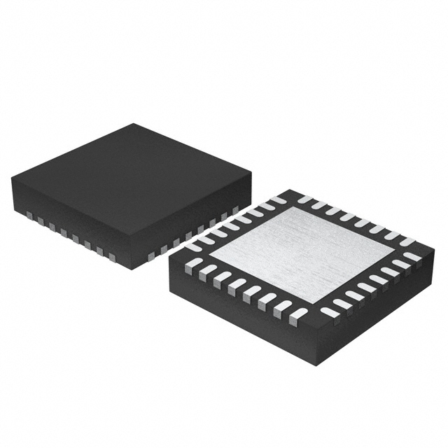
9DML4493A
Datasheet
Description
Features
The 9DML4493A is a 4-input, 4-output clock multiplexer. It can
also operate as a dual 2-input, 2-output clock multiplexer. It has
very low additive phase jitter and is suitable for all PCIe data
rates. Pin straps configure the device, making it ideal for
applications where a serial configuration bus is not available.
▪ Four differential inputs support LVPECL, LVDS, HCSL or
The device supports today's complex system power sequencing
requirements with Power Down Tolerant and Flexible Power
Sequencing features.
▪ Power-Down Tolerant (PDT) inputs: CLK_SEL_tri, OE pins,
LVCMOS reference clocks
▪ Flexible Power Sequencing (FPS) ensures good behavior
when powered up without input clock, or when the input clock
is present without power
IOA_tri, IOB_tri, ZOUTSEL may be driven when the 9DML4493
is not powered up
▪ Accepts input frequencies ranging from 1PPS (1Hz) to 350MHz
▪ Strapping pin selects differential output impedances of 100Ω or
Typical Applications
▪
▪
▪
▪
▪
85Ω, saving up to 16 resistors
Servers
Storage
Networking
High-Performance computing
Accelerators
▪
▪
▪
▪
▪
▪
▪
Key Specifications
▪ Additive phase jitter:
Three pin-selectable output amplitudes per bank
Pin selectable 4:4 mode or dual 2:2 MUX mode
Glitch-free output enable pins for each output
Spread spectrum tolerant
Voltage supply of 1.8V, 2.5V, or 3.3V
-40°C to +85°C ambient operating temperature
5 × 5 mm 32-VFQFPN package
• 12fs RMS typical (PCIe Gen5 CC at 100MHz)
• 66fs RMS typical (12kHz–20MHz at 156.25M)
▪ Supports PCIe Gen1–5 PCIe Refclk requirements
▪ Supports PCIe CC and IR (SRIS, SRNS) timing architectures
▪ Propagation delay < 1.2ns typical
Block Diagram
VDDCLK x4
vOEA[1:0]
^vCLK_SEL_tri[1:0]
VDDCORE
VDDOA
VDDOB
2
2
CLKA0
CLKA0#
CLKIN0
CLKIN0#
CLKIN3
CLKIN3#
CLKA1
CLKA1#
CLKIN1
CLKIN1#
CLKB0
CLKB0#
CLKIN2
CLKIN2#
CLKB1
CLKB1#
vOEB[1:0]
^vIOA_tri
^vIOB_tri
^ZOUTSEL
2
Logic
EPAD is GND
©2021 Renesas Electronics Corporation
1
February 19, 2021
�9DML4493A Datasheet
Contents
Description . . . . . . . . . . . . . . . . . . . . . . . . . . . . . . . . . . . . . . . . . . . . . . . . . . . . . . . . . . . . . . . . . . . . . . . . . . . . . . . . . . . . . . . . . . . . . . . . . . . . . . 1
Typical Applications . . . . . . . . . . . . . . . . . . . . . . . . . . . . . . . . . . . . . . . . . . . . . . . . . . . . . . . . . . . . . . . . . . . . . . . . . . . . . . . . . . . . . . . . . . . . . . . 1
Key Specifications . . . . . . . . . . . . . . . . . . . . . . . . . . . . . . . . . . . . . . . . . . . . . . . . . . . . . . . . . . . . . . . . . . . . . . . . . . . . . . . . . . . . . . . . . . . . . . . . 1
Features . . . . . . . . . . . . . . . . . . . . . . . . . . . . . . . . . . . . . . . . . . . . . . . . . . . . . . . . . . . . . . . . . . . . . . . . . . . . . . . . . . . . . . . . . . . . . . . . . . . . . . . . 1
Block Diagram . . . . . . . . . . . . . . . . . . . . . . . . . . . . . . . . . . . . . . . . . . . . . . . . . . . . . . . . . . . . . . . . . . . . . . . . . . . . . . . . . . . . . . . . . . . . . . . . . . . 1
Pin Assignments. . . . . . . . . . . . . . . . . . . . . . . . . . . . . . . . . . . . . . . . . . . . . . . . . . . . . . . . . . . . . . . . . . . . . . . . . . . . . . . . . . . . . . . . . . . . . . . . . . 3
Clock Input Bias Network . . . . . . . . . . . . . . . . . . . . . . . . . . . . . . . . . . . . . . . . . . . . . . . . . . . . . . . . . . . . . . . . . . . . . . . . . . . . . . . . . . . . . . 3
Pin Descriptions . . . . . . . . . . . . . . . . . . . . . . . . . . . . . . . . . . . . . . . . . . . . . . . . . . . . . . . . . . . . . . . . . . . . . . . . . . . . . . . . . . . . . . . . . . . . . . . . . . 4
Absolute Maximum Ratings . . . . . . . . . . . . . . . . . . . . . . . . . . . . . . . . . . . . . . . . . . . . . . . . . . . . . . . . . . . . . . . . . . . . . . . . . . . . . . . . . . . . . . . . . 6
Electrical Characteristics . . . . . . . . . . . . . . . . . . . . . . . . . . . . . . . . . . . . . . . . . . . . . . . . . . . . . . . . . . . . . . . . . . . . . . . . . . . . . . . . . . . . . . . . . . . 7
Test Loads . . . . . . . . . . . . . . . . . . . . . . . . . . . . . . . . . . . . . . . . . . . . . . . . . . . . . . . . . . . . . . . . . . . . . . . . . . . . . . . . . . . . . . . . . . . . . . . . . . . . . 19
Alternate Terminations . . . . . . . . . . . . . . . . . . . . . . . . . . . . . . . . . . . . . . . . . . . . . . . . . . . . . . . . . . . . . . . . . . . . . . . . . . . . . . . . . . . . . . . . . . . . 19
Phase Jitter Test Loads . . . . . . . . . . . . . . . . . . . . . . . . . . . . . . . . . . . . . . . . . . . . . . . . . . . . . . . . . . . . . . . . . . . . . . . . . . . . . . . . . . . . . . . . . . . 20
Package Outline Drawings . . . . . . . . . . . . . . . . . . . . . . . . . . . . . . . . . . . . . . . . . . . . . . . . . . . . . . . . . . . . . . . . . . . . . . . . . . . . . . . . . . . . . . . . . 21
Thermal Characteristics . . . . . . . . . . . . . . . . . . . . . . . . . . . . . . . . . . . . . . . . . . . . . . . . . . . . . . . . . . . . . . . . . . . . . . . . . . . . . . . . . . . . . . . . . . . 21
Marking Diagram . . . . . . . . . . . . . . . . . . . . . . . . . . . . . . . . . . . . . . . . . . . . . . . . . . . . . . . . . . . . . . . . . . . . . . . . . . . . . . . . . . . . . . . . . . . . . . . . 21
Ordering Information . . . . . . . . . . . . . . . . . . . . . . . . . . . . . . . . . . . . . . . . . . . . . . . . . . . . . . . . . . . . . . . . . . . . . . . . . . . . . . . . . . . . . . . . . . . . . 21
Revision History . . . . . . . . . . . . . . . . . . . . . . . . . . . . . . . . . . . . . . . . . . . . . . . . . . . . . . . . . . . . . . . . . . . . . . . . . . . . . . . . . . . . . . . . . . . . . . . . . 22
©2021 Renesas Electronics Corporation
2
February 19, 2021
�9DML4493A Datasheet
Pin Assignments
CLKIN1#
CLKIN1
vOEB0
VDDCLK1
CLKIN0#
VDDCLK0
vOEA0
CLKIN0
Figure 1. Pin Assignments for 5 × 5 mm 32-VFQFPN Package – Top View
32 31 30 29 28 27 26 25
vOEA1
^vIOA_tri
CLKA0
CLKA0#
VDDO_A
CLKA1
1
2
3
4
5
6
9DML4493
Connect EPAD to
GND
CLKA1# 7
^vCLK_SEL0_tri 8
24 vOEB1
23 ^vIOB_tri
22 CLKB0
21 CLKB0#
20 VDDO_B
19 CLKB1
18 CLKB1#
17 ^vCLK_SEL1_tri
CLKIN2#
CLKIN2
^ZOUTSEL
VDDCLK2
CLKIN3#
VDDCLK3
VDDCORE
CLKIN3
9 10 11 12 13 14 15 16
32-pin VFQFPN, 5 x 5 mm, 0.5mm pitch
^ prefix indicates internal pull-up resistor
v prefix indicates internal pull-down resistor
^v prefix indicates internal pull-up and pull-down resistor biasing to VDD/2
Clock Input Bias Network
VDD
50kΩ
CLK_IN#
CLK_IN
50kΩ
©2021 Renesas Electronics Corporation
50kΩ
3
February 19, 2021
�9DML4493A Datasheet
Pin Descriptions
Table 1. Pin Descriptions
Number
Name
Type
Description
1
vOEA1
Input
Active high input for enabling output 1 of bank A. This pin has internal pull-down.
0 =disable output low, 1 = enable output.
2
^vIOA_tri
Input
Sets nominal amplitude of Bank A outputs. This is a tri-level input with internal pull-up and
pull down resistors. See Output Amplitude Select, High Impedance Loads table for details.
3
CLKA0
Output
True output of bank A clock 0.
4
CLKA0#
Output
Complementary output of bank A clock 0.
5
VDDO_A
Power
Power supply for output group A.
6
CLKA1
Output
True output of bank A clock 1.
7
CLKA1#
Output
Complementary output of bank A clock 1.
8
^vCLK_SEL0_tri
Input
Input clock selection pin. This is a tri-level input with internal pull-up and pull-down resistors
that bias the pin to VDD/2 when left open. See the Input Select table for details.
9
CLKIN3
Input
True side of differential input clock 3.
10
CLKIN3#
Input
Complementary side of differential input clock 3.
11
VDDCLK3
Power
Power supply for clock input 3.
12
VDDCORE
Power
Power supply for core logic.
13
^ZOUTSEL
Input
Input to select differential output impedance. This input has an internal pull-up resistor. See
the Output Impedance Select table for details.
14
VDDCLK2
Power
Power supply for clock input 2.
15
CLKIN2#
Input
Complementary side of differential input clock 2.
16
CLKIN2
Input
True side of differential input clock 2.
17
^vCLK_SEL1_tri
Input
Input clock selection pin. This is a tri-level input with internal pull-up and pull-down resistors
that bias the pin to VDD/2 when left open. See the Input Select table for details.
18
CLKB1#
Output
Complementary output of bank B clock 1.
19
CLKB1
Output
True output of bank B clock 1.
20
VDDO_B
Power
Power supply for output group B.
21
CLKB0#
Output
Complementary output of bank B clock 0.
22
CLKB0
Output
True output of bank B clock 0.
23
^vIOB_tri
Input
Sets nominal amplitude of Bank B outputs. This is a tri-level input with internal pull-up and
pull-down resistors. See Output Amplitude Select, High Impedance Loads table for details.
24
vOEB1
Input
Active high input for enabling output 1 of bank B. This pin has internal pull-down.
0 = disable output low, 1 = enable output.
25
CLKIN1
Input
True side of differential input clock 1.
26
CLKIN1#
Input
Complementary side of differential input clock 1.
27
VDDCLK1
Power
Power supply for clock input 1.
28
vOEB0
Input
Active high input for enabling output 0 of bank B. This pin has internal pull-down.
0 = disable output low, 1 = enable output.
©2021 Renesas Electronics Corporation
4
February 19, 2021
�9DML4493A Datasheet
Table 1. Pin Descriptions (Cont.)
Number
Name
Type
Description
29
vOEA0
Input
Active high input for enabling output 0 of bank A. This pin has internal pull-down.
0 =disable output low, 1 = enable output.
30
VDDCLK0
Power
Power supply for clock input 0.
31
CLKIN0#
Input
Complementary side of differential input clock 0.
32
CLKIN0
Input
True side of differential input clock 0.
33
EPAD
GND
Connect to ground.
Table 2. Power Management
OExx Pin
CLKINx
1
0
CLKA[1:0], CLKB[1:0]
True Output
Complementary Output
Running
Running
Running
Running
Low
Low
Table 3. Power Connections
Pin Number
Description
VDD
GND
5
33 (EPAD)
Output Bank A
11
33 (EPAD)
Input CLK3
12
33 (EPAD)
Core Logic
14
33 (EPAD)
Input CLK2
20
33 (EPAD)
Output Bank B
27
33 (EPAD)
Input CLK1
30
33 (EPAD)
Input CLK0
CLK_SEL0_tri
CLK_SEL1_tri
Description
0
0
CLK0 drives Bank A and B.
0
1
CLK1 drives Bank A and B.
1
0
CLK2 drives Bank A and B.
1
1
CLK3 drives Bank A and B.
M
M
Reserved.
M
0
CLK0 drives Bank A and CLK1 drives Bank B.
Table 4. Input Select
©2021 Renesas Electronics Corporation
5
February 19, 2021
�9DML4493A Datasheet
Table 4. Input Select
CLK_SEL0_tri
CLK_SEL1_tri
Description
M
1
CLK0 drives Bank A and CLK2 drives Bank B.
0
M
CLK3 drives Bank A and CLK1 drives Bank B.
1
M
CLK3 drives Bank A and CLK2 drives Bank B.
Table 5. Output Impedance Select
ZOUTSEL
Differential Output Impedance (Ω)
0
85 (42.5 single-ended)
1
100 (50 single-ended)
Table 6. Output Amplitude Select, High Impedance Loads
IOA_tri, IOB_tri
2.5V or 3.3V Operation
1.8V Operation
M
750mV nominal Vhigh
700mV nominal Vhigh
0
825mV nominal Vhigh
750mV nominal Vhigh
1
925mV nominal Vhigh
825mV nominal Vhigh
Absolute Maximum Ratings
The absolute maximum ratings are stress ratings only. Stresses greater than those listed below can cause permanent damage to the
device. Functional operation of the 9DML4493A at absolute maximum ratings is not implied. Exposure to absolute maximum rating
conditions may affect device reliability.
Table 7. Absolute Maximum Ratings
Parameter
Symbol
Supply Voltage
VDDx
Input Voltage
VIN
Continuous Current
IO
Surge Current
IO
Storage Temperature
Minimum
Typical
Maximum
Units
Notes
-
-
3.63
V
1,2
-0.5
-
VDD + 0.5
V
1
CLK output pins.
-
-
40
mA
1
CLK output pins.
-
-
60
mA
1
TS
-65
-
150
°C
1
Junction Temperature
TJ
-
-
125
°C
1
Soldering Temperature
TLD
-
-
260
°C
1
Input ESD Protection
ESD Prot
2000
-
-
V
1
1 Guaranteed
2
Conditions
With respect to ground.
10 seconds maximum.
Human Body Model.
by design and characterization, not 100% tested in production.
Operation under these conditions is neither implied nor guaranteed.
©2021 Renesas Electronics Corporation
6
February 19, 2021
�9DML4493A Datasheet
Electrical Characteristics
TA = TAMB, supply voltages per normal operation conditions. See Test Loads for loading conditions.
Table 8. PCIe Refclk Jitter
Parameter
Additive PCIe Refclk Jitter
(Common Clocked
Architecture)
VDD = 1.8V
Additive PCIe Refclk Jitter
(Common Clocked
Architecture)
VDD = 2.5V or 3.3V
Additive PCIe Refclk Jitter
(SRIS Architecture)
VDD = 1.8V
Additive PCIe Refclk Jitter
(SRIS Architecture)
VDD = 2.5V or 3.3V
1
2
3
4
5
Symbol
Conditions
Units
Notes
tjphPCIeG1-CC
PCIe Gen 1 (2.5 GT/s)
—
1.1
2.08
86
ps (p-p)
1,2
PCIe Gen 2 Lo Band (5.0 GT/s)
—
0.020
0.033
3.1
ps (RMS)
1,2
PCIe Gen 2 Hi Band (5.0 GT/s)
—
0.080
0.140
3
ps (RMS)
1,2
tjphPCIeG3-CC
PCIe Gen 3 (8.0 GT/s)
—
0.043
0.071
1
ps (RMS)
1,2,3
tjphPCIeG4-CC
PCIe Gen 4 (16.0 GT/s)
—
0.043
0.071
0.4
ps (RMS) 1,2,3,4
tjphPCIeG5-CC
PCIe Gen 5 (32.0 GT/s)
—
0.017
0.028
0.08
ps (RMS) 1,2,3,5
tjphPCIeG1-CC
PCIe Gen 1 (2.5 GT/s)
—
0.750
1.100
86
ps (p-p)
1,2
PCIe Gen 2 Lo Band (5.0 GT/s)
—
0.016
0.021
3.1
ps (RMS)
1,2
PCIe Gen 2 Hi Band (5.0 GT/s)
—
0.060
0.100
3
ps (RMS)
1,2
tjphPCIeG3-CC
PCIe Gen 3 (8.0 GT/s)
—
0.031
0.041
1
ps (RMS)
1,2,3
tjphPCIeG4-CC
PCIe Gen 4 (16.0 GT/s)
—
0.031
0.041
0.4
ps (RMS) 1,2,3,4
tjphPCIeG5-CC
PCIe Gen 5 (32.0 GT/s)
—
0.012
0.016
0.08
ps (RMS) 1,2,3,5
tjphPCIeG1-SRIS
PCIe Gen 1 (2.5 GT/s)
—
0.120
0.200
N/A
ps (RMS)
1,2,6
tjphPCIeG2-SRIS
PCIe Gen 2 (5.0 GT/s)
—
0.100
0.200
N/A
ps (RMS)
1,2,6
tjphPCIeG3-SRIS
PCIe Gen 3 (8.0 GT/s)
—
0.027
0.044
N/A
ps (RMS)
1,2,6
tjphPCIeG4-SRIS
PCIe Gen 4 (16.0 GT/s)
—
0.028
0.046
N/A
ps (RMS)
1,2,6
tjphPCIeG5-SRIS
PCIe Gen 5 (32.0 GT/s)
—
0.021
0.027
N/A
ps (RMS)
1,2,6
tjphPCIeG1-SRIS
PCIe Gen 1 (2.5 GT/s)
—
0.090
0.120
N/A
ps (RMS)
1,2,6
tjphPCIeG2-SRIS
PCIe Gen 2 (5.0 GT/s)
—
0.080
0.100
N/A
ps (RMS)
1,2,6
tjphPCIeG3-SRIS
PCIe Gen 3 (8.0 GT/s)
—
0.020
0.026
N/A
ps (RMS)
1,2,6
tjphPCIeG4-SRIS
PCIe Gen 4 (16.0 GT/s)
—
0.025
0.041
N/A
ps (RMS)
1,2,6
tjphPCIeG5-SRIS
PCIe Gen 5 (32.0 GT/s)
—
0.018
0.024
N/A
ps (RMS)
1,2,6
tjphPCIeG2-CC
tjphPCIeG2-CC
Minimum Typical Maximum Limit
The Refclk jitter is measured after applying the filter functions found in PCI Express Base Specification 5.0, Revision 1.0. See the Test Loads section
of the data sheet for the exact measurement setup. Values for the Common Clock architecture are calculated with spread off and spread on at
-0.5%. SRIS values are calculated for spread off and spread on at ≤-0.3%. The worst case results for each data rate are summarized in this table.
If oscilloscope data is used, equipment noise is removed from all results. See Test Load for PCIe Phase Jitter Measurements.
Jitter measurements shall be made with a capture of at least 100,000 clock cycles captured by a real-time oscilloscope (RTO) with a sample rate
of 20GS/s or greater. Broadband oscilloscope noise must be minimized in the measurement. The measured PP jitter is used (no extrapolation) for
RTO measurements. Alternately, Jitter measurements may be made with a Phase Noise Analyzer (PNA) extending (flat) and integrating and folding
the frequency content up to an offset from the carrier frequency of at least 200MHz (at 300MHz absolute frequency) below the Nyquist frequency.
For PNA measurements for the 2.5 GT/s data rate, the RMS jitter is converted to peak to peak jitter using a multiplication factor of 8.83. In the case
where real-time oscilloscope and PNA measurements have both been done and produce different results, the RTO result must be used.
SSC spurs from the fundamental and harmonics are removed up to a cutoff frequency of 2MHz taking care to minimize removal of any non-SSC
content.
Note that 0.7ps RMS is to be used in channel simulations to account for additional noise in a real system.
Note that 0.25ps RMS is to be used in channel simulations to account for additional noise in a real system.
©2021 Renesas Electronics Corporation
7
February 19, 2021
�9DML4493A Datasheet
6
The PCI Express Base Specification 5.0, Revision 1.0 provides the filters necessary to calculate SRIS jitter values, however, it does not provide
specification limits, hence the n/a in the Limit column. SRIS values are informative only. In general, a clock operating in an SRIS system must be
twice as good as a clock operating in a Common Clock system. For RMS values, twice as good is equivalent to dividing the CC value by √2. And
additional consideration is the value for which to divide by √2. The conservative approach is to divide the ref clock jitter limit, and the case can be
made for dividing the channel simulation values by √2, if the ref clock is close to the Tx clock input. An example for Gen4 is as follows. A
“rule-of-thumb” SRIS limit would be either 0.5ps RMS/√2 = 0.35ps RMS if the clock chip is far from the clock input, or 0.7ps RMS/√2 = 0.5ps RMS
if the clock chip is near the clock input.
Table 9. Random Phase Jitter
Parameter
Symbol
tjph100M
Additive Phase Jitter
tjph156M
1
2
3
Conditions
Minimum Typical
Maximum
Units
Notes
100MHz, 12kHz to 20MHz, VDD = 1.8V
—
97
158
fs (rms) 1,2,3
100MHz, 12kHz to 20MHz, VDD = 2.5V or 3.3V
—
78
111
fs (rms) 1,2,3
156.25MHz, 12kHz to 20MHz, VDD = 1.8V
—
66
91
fs (rms) 1,2,3
156.25MHz, 12kHz to 20MHz, VDD = 2.5V or 3.3V
—
58
71
fs (rms) 1,2,3
Guaranteed by design and characterization, not 100% tested in production.
Driven by Rhode & Schwartz SMA100.
For RMS figures, additive jitter is calculated by solving the following equation: Additive jitter = SQRT[(total jitter)^2 - (input jitter)^2].
Table 10. Channel to Channel Isolation
Parameter
Symbol
Channel to Channel Isolation
tISO
1
2
Conditions
Minimum
Typical
Maximum
Units
Notes
1.8V operation.
-58
—
—
dBc
1, 2
2.5V or 3.3Voperation.
-66
—
—
dBc
1, 2
Guaranteed by design and characterization, not 100% tested in production.
Measured with 3 channels at 100MHz non-spreading and one channel at 100MHz, -0.5% spread. Value represents worst case combination of inputs
and outputs.
Table 11. Input/Supply/Common Parameters
Parameter
Supply Voltage
Symbol
VDDx
Conditions
Minimum
Typical
Maximum
Units Notes
Supply voltage for core and outputs, 3.3V operation.
3.135
3.3
3.465
V
Supply voltage for core and outputs, 2.5V operation.
2.375
2.5
2.625
V
Supply voltage for core and outputs, 1.8V operation.
1.71
1.8
1.89
V
Industrial range.
-40
25
85
°C
Ambient Operating
Temperature
TAMB
Input High Voltage
VIH
Single-ended inputs, except SMBus.
0.75 VDD
—
VDD + 0.3
V
Input Low Voltage
VIL
Single-ended inputs, except SMBus.
-0.3
—
0.25 VDD
V
IIN
Single-ended inputs, VIN = GND, VIN = VDD.
-5
—
5
μA
IINP
Single-ended inputs.
VIN = 0 V; inputs with internal pull-up resistors.
VIN = VDD; inputs with internal pull-down resistors.
-150
—
150
μA
Input Current
©2021 Renesas Electronics Corporation
8
February 19, 2021
�9DML4493A Datasheet
Table 11. Input/Supply/Common Parameters (Cont.)
Parameter
Symbol
Input Frequency
FIN
PPM Error
fERROR
DC Output
Impedance
ZO-DC
Pin Inductance
Lpin
Conditions
Minimum
Typical
Maximum
1 PPS
—
350
Input to output ppm error.
Units Notes
0
MHz
4
ppm
5
85Ω setting (single-ended value).
34
42.5
51
Ω
1
100Ω setting (single-ended value).
40
50
60
Ω
1
—
—
7
nH
1
Logic inputs, including CLK.
2.2
2.8
3.2
pF
1
COUT
Output pin capacitance.
—
—
6
pF
1
Clk Stabilization
TSTAB
From VDD reaching 90% of target, input clock
present.
—
—
3
ms
1,2
Input SS Modulation
Frequency PCIe
fMODINPCIe
Allowable frequency for PCIe applications
(Triangular modulation)
30
31.5
33
kHz
OE Latency
tLATOE
Q start after OE assertion.
Q stop after OE deassertion.
2
—
10
clocks
1,3
Tfall
tF
Fall time of single-ended control inputs.
—
—
5
ns
2
Trise
tR
Rise time of single-ended control inputs.
—
—
5
ns
2
CIN
Capacitance
1
2
3
4
5
Guaranteed by design and characterization, not 100% tested in production.
Control input must be monotonic from 20% to 80% of input swing.
Time from deassertion until outputs are > 200mV.
“PPS” means Pulse Per Second or Hertz.
This device does not alter the ppm accuracy of the input clock.
Table 12. Source-Terminated LP-HCSL Driver with High-Impedance Receiver
TAMB = over the specified operating range. Supply voltages per normal operation conditions. See Test Loads for loading conditions.
Parameter
Symbol
Conditions
Minimum Typical Maximum
Limit
Units
Notes
Rising/Falling Slew Rate
dV/dt
1.4
2.3
3.2
1 to 4
V/ns
2, 3,10
Rising Edge (REFCLK+) to Falling Edge
(REFCLK-) Matching
tR/tF
—
3.2
12
20
%
1,10,12
Absolute Max Output Voltage
VMAX
—
—
900
1150
mV
1, 7, 10
Absolute Min Output Voltage
VMIN
-142
—
—
-300
mV
1, 8, 10
Output High Voltage
VOH
564
708
881
N/A
mV
1,7
Output Low Voltage
VOL
-104
-6
99
N/A
mV
1,8
255
355
446
250 to 550
mV
1, 4,
5,10
—
28
124
140
mV
1, 4, 9,
10
Absolute Crossing Point Voltage
100MHz,
IOA_tri,
IOB_tri = M
VDD = 1.8V
VCROSS
VCROSS Variation over all Rising Clock Edges VCROSS
©2021 Renesas Electronics Corporation
9
February 19, 2021
�9DML4493A Datasheet
Table 12. Source-Terminated LP-HCSL Driver with High-Impedance Receiver (Cont.)
TAMB = over the specified operating range. Supply voltages per normal operation conditions. See Test Loads for loading conditions.
Parameter
Symbol
Conditions
Minimum Typical Maximum
Limit
Units
Notes
Rising/Falling Slew Rate
dV/dt
1.7
2.5
3.5
1 to 4
V/ns
2, 3,10
Rising Edge (REFCLK+) to Falling Edge
(REFCLK-) Matching
tR/tF
—
3.1
12
20
%
1,10,12
Absolute Max Output Voltage
VMAX
—
—
990
1150
mV
1, 7,10
-157
—
—
-300
mV
1, 8,10
614
766
969
N/A
mV
1, 7
-121
-10
96
N/A
mV
1, 8
285
380
490
250 to 550
mV
1, 4,
5,10
VCROSS Variation over all Rising Clock Edges VCROSS
—
29
107
140
mV
1, 4, 9,
10
Rising/Falling Slew Rate
dV/dt
1.6
2.6
3.9
1 to 4
V/ns
2, 3, 10
Rising Edge (REFCLK+) to Falling Edge
(REFCLK-) Matching
tR/tF
—
3.3
12
20
%
1,10,12
Absolute Max Output Voltage
VMAX
—
—
1093
1150
mV
1, 7,10
Absolute Min Output Voltage
VMIN
-175
—
—
-300
mV
1, 8,10
Output High Voltage
VOH
650
825
1069
N/A
mV
1, 7
Output Low Voltage
VOL
-130
-14
101
N/A
mV
1, 8
303
403
512
250 to 550
mV
1, 4, 5,
10
VCROSS Variation over all Rising Clock Edges VCROSS
—
31
119
140
mV
1, 4, 9,
10
Rising/Falling Slew Rate
dV/dt
2.0
2.5
3.3
1 to 4
V/ns
2, 3,10
Rising Edge (REFCLK+) to Falling Edge
(REFCLK-) Matching
tR/tF
—
3.3
10
20
%
1,10,12
Absolute Max Output Voltage
VMAX
—
—
932
1150
mV
1, 7,10
Absolute Min Output Voltage
VMIN
-162
—
—
-300
mV
1, 8,10
Output High Voltage
VOH
616
749
906
N/A
mV
1, 7
Output Low Voltage
VOL
-119
-22
79
N/A
mV
1, 8
279
372
463
250 to 550
mV
1, 4,
5,10
—
32
125
140
mV
1, 4, 9,
10
Absolute Min Output Voltage
VMIN
Output High Voltage
VOH
Output Low Voltage
VOL
Absolute Crossing Point Voltage
Absolute Crossing Point Voltage
Absolute Crossing Point Voltage
100MHz,
IOA_tri,
IOB_tri = 0
VDD = 1.8V
VCROSS
100MHz,
IOA_tri,
IOB_tri = 1
VDD = 1.8V
VCROSS
100MHz,
IOA_tri,
IOB_tri = M
VDD = 2.5V or
3.3V
VCROSS
VCROSS Variation over all Rising Clock Edges VCROSS
©2021 Renesas Electronics Corporation
10
February 19, 2021
�9DML4493A Datasheet
Table 12. Source-Terminated LP-HCSL Driver with High-Impedance Receiver (Cont.)
TAMB = over the specified operating range. Supply voltages per normal operation conditions. See Test Loads for loading conditions.
Parameter
Symbol
Conditions
Minimum Typical Maximum
Limit
Units
Notes
Rising/Falling Slew Rate
dV/dt
2.1
2.8
3.6
1 to 4
V/ns
2, 3, 10
Rising Edge (REFCLK+) to Falling Edge
(REFCLK-) Matching
tR/tF
—
3.4
10
20
%
1,10,12
Absolute Max Output Voltage
VMAX
—
—
1007
1150
mV
1, 7, 10
Absolute Min Output Voltage
VMIN
-175
—
—
-300
mV
1, 8, 10
Output High Voltage
VOH
700
827
979
N/A
mV
1, 7
Output Low Voltage
VOL
-136
-27
93
N/A
mV
1, 8
311
405
464
250 to 550
mV
1, 4, 5,
10
VCROSS Variation over all Rising Clock Edges VCROSS
—
36
128
140
mV
1, 4, 9,
10
Rising/Falling Slew Rate
dV/dt
2.3
3.0
3.9
1 to 4
V/ns
2, 3, 10
Rising Edge (REFCLK+) to Falling Edge
(REFCLK-) Matching
tR/tF
—
3.5
10
20
%
1, 10,
12
Absolute Max Output Voltage
VMAX
—
—
1097
1150
mV
1, 7, 10
Absolute Min Output Voltage
VMIN
-191
—
—
-300
mV
1, 8, 10
Output High Voltage
VOH
807
917
1075
N/A
mV
1, 7
Output Low Voltage
VOL
-149
-30
98
N/A
mV
1, 8
347
439
503
250 to 550
mV
1, 4, 5,
10
—
39
137
140
mV
1, 4, 9,
10
Absolute Crossing Point Voltage
Absolute Crossing Point Voltage
100MHz,
IOA_tri,
IOB_tri = 0
VDD = 2.5V or
3.3V
VCROSS
100MHz,
IOA_tri,
IOB_tri = 1
VDD = 2.5V or
3.3V
VCROSS
VCROSS Variation over all Rising Clock Edges VCROSS
1
2
3
Measurement taken from single-ended waveform.
Measurement taken from differential waveform.
Measured from -75mV to +75mV on the differential waveform (derived from REFCLK+ minus REFCLK-). The signal must be monotonic through
the measurement region for rise and fall time. The 150 mV measurement window is centered on the differential zero crossing. See Figure 6
“Rise/Fall Measurement Points (Differential Waveform)”.
4 Measured at crossing point where the instantaneous voltage value of the rising edge of REFCLK+ equals the falling edge of REFCLK-. See Figure
5
“Absolute Cross Point and Swing Measurement Points (Single-ended Waveform)”.
2
Refers to the total variation from the lowest crossing point to the highest, regardless of which edge is crossing. Refers to all crossing points for this
measurement. See Figure 2 “Absolute Cross Point and Swing Measurement Points (Single-ended Waveform)”.
6 Defines as the absolute minimum or maximum instantaneous period. This includes cycle to cycle jitter, relative PPM tolerance, and spread spectrum
7
8
9
modulation. See Figure 5 “Duty Cycle and Clock Period Measurement Points (Differential Waveform)”.
Defined as the maximum instantaneous voltage including overshoot. See Figure 2 “Absolute Cross Point and Swing Measurement Points
(Single-ended Waveform)”.
Defined as the minimum instantaneous voltage including undershoot. See Figure 2 “Absolute Cross Point and Swing Measurement Points
(Single-ended Waveform)”.
Defined as the total variation of all crossing voltages of Rising REFCLK+ and Falling REFCLK-. This is the maximum allowed variance in VCROSS
for any particular system. See Figure 3 “VCROSSDELTA Measurement Points (Single-ended Waveform)”.
10
System board compliance measurements must use the test load card. REFCLK+ and REFCLK- are to be measured at the load capacitors CL.
Single ended probes must be used for measurements requiring single ended measurements. Either single ended probes with math or differential
probe can be used for differential measurements. Test load CL = 2pF.
©2021 Renesas Electronics Corporation
11
February 19, 2021
�9DML4493A Datasheet
11
12
PPM refers to parts per million and is a DC absolute period accuracy specification. 1PPM is 1/1,000,000th of 100.000000MHz exactly or 100Hz.
For example for 300PPM, then we have an error budget of 100Hz/PPM × 300PPM = 30kHz. The period is to be measured with a frequency counter
with measurement window set to 100ms or greater.
Matching applies to rising edge rate for REFCLK+ and falling edge rate for REFCLK-. It is measured using a ±75mV window centered on the
median cross point where REFCLK+ rising meets REFCLK- falling. The median cross point is used to calculate the voltage thresholds the
oscilloscope is to use for the edge rate calculations. The Rise Edge Rate of REFCLK+ should be compared to the Fall Edge Rate of REFCLK-;
the maximum allowed difference should not exceed 20% of the slowest edge rate. See Figure 4 “Rise/Fall Matching Measurement Points
(Single-ended Waveform)”.
Figure 2. Absolute Cross Point and Swing Measurement Points (Single-ended Waveform)
VMAX = 1.15V
REFCLK-
VHIGH
VCROSSMAX
VCROSSMIN
REFCLK+
VMIN = -0.30V
Figure 3. VCROSSDELTA Measurement Points (Single-ended Waveform)
REFCLKVCROSSDELTA
REFCLK+
Figure 4. Rise/Fall Matching Measurement Points (Single-ended Waveform)
REFCLK-
REFCLK-
VCROSSMEDIAN
VCROSSMEDIAN +75mV
VCROSSMEDIAN
VCROSSMEDIAN -75mV
REFCLK+
REFCLK+
TFALL
TRISE
Figure 5. Duty Cycle and Clock Period Measurement Points (Differential Waveform)
Clock Period (differential)
Positive Duty Cycle
(differential)
0.0V
REFCLK+
Minus
REFCLK-
©2021 Renesas Electronics Corporation
12
February 19, 2021
�9DML4493A Datasheet
Figure 6. Rise/Fall Measurement Points (Differential Waveform)
Rising Edge Rate
Falling Edge Rate
VIH = +150mV
0.0V
VIL = -150mV
REFCLK+
Minus
REFCLKTable 13. Source-Terminated LP-HCSL Driver with Receiver Terminated Load (Double-Terminated)
TAMB = over the specified operating range. Supply voltages per normal operation conditions. See Test Loads for loading conditions.
Parameter
Symbol
Conditions
Minimum
Typical
Maximum
Limit
Units
Notes
Rising/Falling Slew Rate
dV/dt
1.7
2.6
3.6
1 to 4
V/ns
2, 3,10
Rising Edge (REFCLK+) to Falling Edge
(REFCLK-) Matching
tR/tF
—
3
14
20
%
1, 11,
12
Absolute Max Output Voltage
VMAX
—
—
453
575
mV
1, 7,10
Absolute Min Output Voltage
VMIN
-27
—
—
-150
mV
1, 8,10
Output High Voltage
VOH
289
367
441
N/A
mV
1, 7
Output Low Voltage
VOL
-17
10
38
N/A
mV
1, 8
VCROSS
138
188
246
125 to 275
mV
1, 4, 5,
10
VCROSS
—
11
48
70
mV
1, 4, 9,
10
Rising/Falling Slew Rate
dV/dt
1.8
2.8
4.1
1.5 to 4.5
V/ns
2, 3,10
Rising Edge (REFCLK+) to Falling Edge
(REFCLK-) Matching
tR/tF
—
3
13
20
%
1, 11,
12
Absolute Max Output Voltage
VMAX
—
—
492
575
mV
1, 7, 10
Absolute Min Output Voltage
VMIN
-27
—
—
-150
mV
1, 8, 10
Output High Voltage
VOH
309
396
478
N/A
mV
1, 7
Output Low Voltage
VOL
-13
10
36
N/A
mV
1, 8
VCROSS
146
201
264
125 to 275
mV
1, 4, 5,
10
VCROSS
—
11
51
70
mV
1, 4, 9,
10
Absolute Crossing Point Voltage
VCROSS Variation over all Rising Clock
Edges
Absolute Crossing Point Voltage
VCROSS Variation over all Rising Clock
Edges
©2021 Renesas Electronics Corporation
100MHz,
IOA_tri,
IOB_tri = M
VDD = 1.8V
100MHz,
IOA_tri,
IOB_tri = 0
VDD = 1.8V
13
February 19, 2021
�9DML4493A Datasheet
Table 13. Source-Terminated LP-HCSL Driver with Receiver Terminated Load (Double-Terminated)
(Cont.)
Parameter
Symbol
Conditions
Minimum
Typical
Maximum
Limit
Units
Notes
Rising/Falling Slew Rate
dV/dt
1.9
3.0
4.3
1.5 to 4.5
V/ns
2, 3, 10
Rising Edge (REFCLK+) to Falling Edge
(REFCLK-) Matching
tR/tF
—
3
15
20
%
1, 11,
12
Absolute Max Output Voltage
VMAX
—
—
535
575
mV
1, 7, 10
Absolute Min Output Voltage
VMIN
-30
—
—
-150
mV
1, 8, 10
Output High Voltage
VOH
317
423
517
N/A
mV
1, 7
Output Low Voltage
VOL
-14
11
37
N/A
mV
1, 8
VCROSS
150
215
286
140 to 290
mV
1, 4, 5,
10
VCROSS
—
12
54
70
mV
1, 4, 9,
10
Rising/Falling Slew Rate
dV/dt
1.9
2.7
3.8
1 to 4
V/ns
2, 3, 10
Rising Edge (REFCLK+) to Falling Edge
(REFCLK-) Matching
tR/tF
—
3
13
20
%
1, 11,
12
Absolute Max Output Voltage
VMAX
—
—
463
575
mV
1, 7, 10
Absolute Min Output Voltage
VMIN
-27
—
—
-150
mV
1, 8, 10
Output High Voltage
VOH
336
391
451
N/A
mV
1, 7
Output Low Voltage
VOL
-14
9
35
N/A
mV
1,8
VCROSS
163
203
254
125 to 275
mV
1, 4, 5,
10
VCROSS
—
11
48
70
mV
1, 4, 9,
10
Rising/Falling Slew Rate
dV/dt
2.2
3.0
4.0
1 to 4
V/ns
2, 3, 10
Rising Edge (REFCLK+) to Falling Edge
(REFCLK-) Matching
tR/tF
—
3
13
20
%
1, 11,
12
Absolute Max Output Voltage
VMAX
—
—
493
575
mV
1, 7, 10
Absolute Min Output Voltage
VMIN
-26
—
—
-150
mV
1, 8, 10
Output High Voltage
VOH
379
429
482
N/A
mV
1, 7
Output Low Voltage
VOL
-13
10
34
N/A
mV
1, 8
VCROSS
182
221
271
125 to 275
mV
1, 4, 5,
10
VCROSS
—
12
50
70
mV
1, 4, 9,
10
Absolute Crossing Point Voltage
VCROSS Variation over all Rising Clock
Edges
Absolute Crossing Point Voltage
VCROSS Variation over all Rising Clock
Edges
Absolute Crossing Point Voltage
VCROSS Variation over all Rising Clock
Edges
©2021 Renesas Electronics Corporation
100MHz,
IOA_tri,
IOB_tri = 1
VDD = 1.8V
100MHz,
IOA_tri,
IOB_tri = M
VDD = 2.5V or
3.3V
100MHz,
IOA_tri,
IOB_tri = 0
VDD = 2.5V or
3.3V
14
February 19, 2021
�9DML4493A Datasheet
Table 13. Source-Terminated LP-HCSL Driver with Receiver Terminated Load (Double-Terminated)
(Cont.)
Parameter
Symbol
Conditions
Minimum
Typical
Maximum
Limit
Units
Notes
Rising/Falling Slew Rate
dV/dt
1.9
3.0
4.5
1.5 to 4.5
V/ns
2, 3, 10
Rising Edge (REFCLK+) to Falling Edge
(REFCLK-) Matching
tR/tF
—
3
13
20
%
1, 11,
12
Absolute Max Output Voltage
VMAX
—
—
529
575
mV
1, 7, 10
Absolute Min Output Voltage
VMIN
-30
—
—
-150
mV
1, 8, 10
Output High Voltage
VOH 1
427
469
511
N/A
mV
1, 7
Output Low Voltage
VOL 1
-11
11
36
N/A
mV
1, 8
VCROSS
200
242
293
150 to 300
mV
1, 4, 5,
10
VCROSS
—
14
57
70
mV
1, 4, 9,
10
Absolute Crossing Point Voltage
VCROSS Variation over all Rising Clock
Edges
1
2
3
100MHz,
IOA_tri,
IOB_tri = 1
VDD = 2.5V or
3.3V
Measurement taken from single-ended waveform.
Measurement taken from differential waveform.
Measured from -75 mV to +75 mV on the differential waveform (derived from REFCLK+ minus REFCLK-). The signal must be monotonic through
the measurement region for rise and fall time. The 150mV measurement window is centered on the differential zero crossing. See Figure 11
“Rise/Fall Measurement Points (Differential Waveform)”.
4 Measured at crossing point where the instantaneous voltage value of the rising edge of REFCLK+ equals the falling edge of REFCLK-. See Figure
5
“Absolute Cross Point and Swing Measurement Points (Single-Ended Waveform)”.
7
Refers to the total variation from the lowest crossing point to the highest, regardless of which edge is crossing. Refers to all crossing points for this
measurement. See Figure 7 “Absolute Cross Point and Swing Measurement Points (Single-Ended Waveform)”.
6 Defines as the absolute minimum or maximum instantaneous period. This includes cycle to cycle jitter, relative PPM tolerance, and spread spectrum
7
8
9
modulation. See Figure 10 “Duty Cycle and Clock Period Measurement Points (Differential Waveform)”.
Defined as the maximum instantaneous voltage including overshoot. See Figure 7 “Absolute Cross Point and Swing Measurement Points
(Single-Ended Waveform)”.
Defined as the minimum instantaneous voltage including undershoot. See Figure 7 “Absolute Cross Point and Swing Measurement Points
(Single-Ended Waveform)”.
Defined as the total variation of all crossing voltages of Rising REFCLK+ and Falling REFCLK-. This is the maximum allowed variance in VCROSS
for any particular system. See Figure 8 “VCROSSDELTA Measurement Points (Single-Ended Waveform)”.
10
11
12
System board compliance measurements must use the test load card. REFCLK+ and REFCLK- are to be measured at the load capacitors CL.
Single ended probes must be used for measurements requiring single ended measurements. Either single ended probes with math or differential
probe can be used for differential measurements. Test load CL = 2pF.
PPM refers to parts per million and is a DC absolute period accuracy specification. 1PPM is 1/1,000,000th of 100.000000MHz exactly or 100Hz.
For example for 300PPM, then we have an error budget of 100Hz/PPM × 300PPM = 30kHz. The period is to be measured with a frequency counter
with measurement window set to 100ms or greater.
Matching applies to rising edge rate for REFCLK+ and falling edge rate for REFCLK-. It is measured using a ±75mV window centered on the
median cross point where REFCLK+ rising meets REFCLK- falling. The median cross point is used to calculate the voltage thresholds the
oscilloscope is to use for the edge rate calculations. The Rise Edge Rate of REFCLK+ should be compared to the Fall Edge Rate of REFCLK-;
the maximum allowed difference should not exceed 20% of the slowest edge rate. See Figure 9 “Rise/Fall Matching Measurement Points
(Single-Ended Waveform)”.
©2021 Renesas Electronics Corporation
15
February 19, 2021
�9DML4493A Datasheet
Figure 7. Absolute Cross Point and Swing Measurement Points (Single-ended Waveform)
VMAX = 0.575V
REFCLK-
VHIGH
VCROSSMAX
VCROSSMIN
REFCLK+
VMIN = -0.15V
Figure 8. VCROSSDELTA Measurement Points (Single-ended Waveform)
REFCLKVCROSSDELTA
REFCLK+
Figure 9. Rise/Fall Matching Measurement Points (Single-ended Waveform)
REFCLK-
REFCLK-
VCROSSMEDIAN
VCROSSMEDIAN +37.5mV
VCROSSMEDIAN
VCROSSMEDIAN -37.5mV
REFCLK+
REFCLK+
TFALL
TRISE
Figure 10. Duty Cycle and Clock Period Measurement Points (Differential Waveform)
Clock Period (differential)
Positive Duty Cycle
(differential)
0.0V
REFCLK+
Minus
REFCLK-
©2021 Renesas Electronics Corporation
16
February 19, 2021
�9DML4493A Datasheet
Figure 11. Rise/Fall Measurement Points (Differential Waveform)
Rising Edge Rate
Falling Edge Rate
VIH = +75mV
0.0V
VIL = -75mV
REFCLK+
Minus
REFCLKTable 14. Differential Clock Input Parameters
Parameter
Symbol
Conditions
Input High Current–CLKINx,
CLKINx#
IIH
VDDCLKx = 3.465V, 2.625V or 1.89V = VIN.
—
—
150
μA
1
VDD = 3.465V, 2.625V or 1.89V, VIN = 0V.
-5
—
—
μA
1
VDD = 3.465V, 2.625V or 1.89V, VIN = 0V.
-150
—
—
μA
1
Single-ended input swing.
0.15
—
1.3
V
2
0.075
—
VDDCLKx – 1.2
V
2,3
Input Low Current–CLKINx
IIL
Input Low Current–CLKINx#
Peak-to-peak Voltage
VP2P
Common Mode Input Voltage
VCMR
1
2
3
Minimum Typical
Maximum
Units Notes
CLKINx denotes input clocks where x = 0 to 3.
VIL should not be less than –0.3V. VIH should not be higher than VDDCLKx.
Common mode voltage is defined as the cross-point.
Table 15. Output Duty Cycle, Jitter, and Skew Characteristics
Parameter
Symbol
Duty Cycle Distortion
tDCD
Skew, Input to Output
Skew, Output to Output
1
Minimum
Typical
Maximum
Units
Notes
Measured differentially at 100MHz.
-0.9
-0.4
0.2
%
1,3
tPD
VT = 50%.
0.73
1.2
1.6
ns
1
tSK3
VT = 50%.
—
4.9
22
ps
1
Guaranteed by design and characterization, not 100% tested in production.
2 Measured
3
Conditions
from differential waveform.
Duty cycle distortion is the difference in duty cycle between the output and the input clock.
Table 16. Current Consumption
Parameter
Operating Supply Current,
VDD = 1.8V
Symbol
IDDCORE
IDDOx
IDDCLKx
Conditions
Minimum
Typical
Maximum
Units
VDDCORE, All outputs active at 100MHz.
—
13
16
mA
Total VDDO, All outputs active at 100MHz.
—
46
60
mA
Total VDDCLK, All CLK inputs active at 100MHz.
—
10
12
mA
©2021 Renesas Electronics Corporation
17
Notes
February 19, 2021
�9DML4493A Datasheet
Table 16. Current Consumption (Cont.)
Parameter
Operating Supply Current,
VDD = 2.5V or 3.3V
Standby Current,
VDD = 1.8V
Standby Current,
VDD = 2.5V or 3.3V
1
Symbol
Minimum
Typical
Maximum
Units
VDDCORE, All outputs active at 100MHz.
—
16
21
mA
Total VDDO, All outputs active at 100MHz.
—
66
82
mA
IDDCLKx
Total VDDCLK, All CLK inputs active at 100MHz.
—
12
16
mA
IDDCORE
VDDCORE, all outputs disabled.
—
13
16
mA
1
Total VDDO, all outputs disabled.
—
24
34
mA
1
IDDCLKx
Total VDDCLKx, all outputs disabled.
—
6
8
mA
1
IDDCORE
VDDCORE, all outputs disabled.
—
16
21
mA
1
Total VDDO, all outputs disabled.
—
35
42
mA
1
Total VDDCLKx, all outputs disabled.
—
7
9
mA
1
IDDCORE
IDDOx
IDDOx
IDDOx
IDDCLKx
Conditions
Notes
CLKINx/CLKINx# set low/low.
©2021 Renesas Electronics Corporation
18
February 19, 2021
�9DML4493A Datasheet
Test Loads
Figure 12. Source-Terminated Driver with High-Impedance Receiver
Rs
CL
L
Diff
Device Zo
Test
Points
Differential Load Zo
CL
Rs
Table 17. Parameters for Source-Terminated Driver with High-Impedance Receiver[a]
ZOUTSEL
Differential Device Zo (Ω)
Rs (Ω)
Differential Load Zo (Ω)
L (Inches)
CL (pF)
0
85
Internal
85
10
2
0
85
External 7.5
100
10
2
1
100
Internal
100
10
2
[a] This load is only used for signal integrity measurements at 100MHz into a 10 inch load (PCIe). Higher frequencies use the Double-Terminated
test load for signal integrity measurements.
Figure 13. Source-Terminated Driver with Receiver Termination (Double-Terminated)
Rs
L
Diff
Device Zo
CL
Rp
Differential Load Zo
Test
Points
Rp
CL
Rs
Table 18. Parameters for Source-Terminated Driver with Receiver Termination (Double Terminated)[a]
ZOUTSEL
Differential Device Zo (Ω)
Rs (Ω)
Differential Load Zo (Ω)
L (Inches)
CL (pF)
RP (pF)
0
85
Internal
85
10
2
42.5
0
85
External 7.5
100
10
2
50
1
100
Internal
100
10
2
50
[a] This load is used for signal integrity measurements at frequencies higher than 100MHz. It may also be used at 100MHz.
Alternate Terminations
The LP-HCSL output can easily drive other logic families. See “AN-891 Driving LVPECL, LVDS, and CML Logic with IDT's “Universal”
Low-Power HCSL Outputs” for termination schemes for LVPECL, LVDS, CML and SSTL.
©2021 Renesas Electronics Corporation
19
February 19, 2021
�9DML4493A Datasheet
Phase Jitter Test Loads
Figure 14. Test Setup for Additive Phase Jitter Measurements
PNA
Coax
Cables
L
CKIN+
CK+
CK+
Zo (differential)
DUT
Clock Source
CKIN-
CK-
Balun
0.1uF
CK-
50
SMA
Connectors
Table 19. Parameters for Phase Jitter Measurements
Clock Source
ZOUTSEL
Differential Device Zo (Ω)
Rs (Ω)
Differential Load Zo (Ω)
L (Inches)
SMA100B
0
85
Internal
85
10
SMA100B
1
100
Internal
100
10
©2021 Renesas Electronics Corporation
20
February 19, 2021
�9DML4493A Datasheet
Package Outline Drawings
The package outline drawings are located at the end of this document. The package information is the most current data available and is
subject to change without revision of this document.
Thermal Characteristics
Table 20. Thermal Characteristics1
Parameter
Thermal Resistance
1
Symbol
Parameter
Package
Value
Units
θJB
Junction to base.
1.9
°C/W
θJC
Junction to case.
34.6
°C/W
θJA0
Junction to Air, still air.
43.5
°C/W
θJA1
Junction to Air, 1 m/s air flow.
36.7
°C/W
θJA3
Junction to Air, 3 m/s air flow.
32.9
°C/W
θJA5
Junction to Air, 5 m/s air flow.
31.4
°C/W
NLG32
EPAD soldered to ground.
Marking Diagram
▪ Lines 2 and 3 indicate the part number.
▪ Line 4 indicates the following:
• “#” denotes the stepping.
• “YY” is the last two digits of the year; “WW” is the work week number when the part
was assembled.
• “$” denotes the mark code.
Ordering Information
Orderable Part Number
Package
Carrier Type
Temperature
9DML4493ANLGI
5 × 5 mm 32-VFQFPN
Tray
-40° to +85°C
9DML4493ANLGI8
5 × 5 mm 32-VFQFPN
Tape and Reel
-40° to +85°C
“G” suffix denotes Pb-free configuration, RoHS compliant.
©2021 Renesas Electronics Corporation
21
February 19, 2021
�9DML4493A Datasheet
Revision History
Revision Date
February 19, 2021
June 17, 2020
Description of Change
▪ Updated 1st page description.
▪ Updated 1st page Features list.
▪ Added Clock Input Bias Network diagram.
▪
▪
▪
▪
▪
Updated footnote 2 on table 10.
Updated Output High Voltage values for 100MHz, IOA_tri, IOB_tri = 0, VDD = 1.8V.
Updated Absolute Max Output Voltage values for 100MHz, IOA_tri, IOB_tri = 1, VDD = 1.8V.
Updated values in tables 8, 12, 13, and 16.
Changed ZOUTSEL from an internal pull-down to an internal pull-up resistor in Block Diagram, Pin
Assignments, and Pin Descriptions.
▪ Corrected pull-up typo in pin descriptions for pin 1, 24, 28, and 29; changed to pull-down.
▪ Updated maximum values for standby and supply current specifications.
June 1, 2020
Re-arranged and updated electrical tables and moved to final.
May 19, 2020
Updated typical values in electrical tables.
May 15, 2020
Updated electrical tables, added typical values and moved to preliminary
April 6, 2020
Initial release.
©2021 Renesas Electronics Corporation
22
February 19, 2021
�32-VFQFPN, Package Outline Drawing
5.0 x 5.0 x 0.90 mm Body, Epad 3.15 x 3.15 mm.
NLG32P1, PSC-4171-01, Rev 02, Page 1
�32-VFQFPN, Package Outline Drawing
5.0 x 5.0 x 0.90 mm Body, Epad 3.15 x 3.15 mm.
NLG32P1, PSC-4171-01, Rev 02, Page 2
Package Revision History
Description
Date Created
Rev No.
April 12, 2018
Rev 02
New Format
Feb 8, 2016
Rev 01
Added "k: Value
�IMPORTANT NOTICE AND DISCLAIMER
RENESAS ELECTRONICS CORPORATION AND ITS SUBSIDIARIES (“RENESAS”) PROVIDES TECHNICAL
SPECIFICATIONS AND RELIABILITY DATA (INCLUDING DATASHEETS), DESIGN RESOURCES (INCLUDING
REFERENCE DESIGNS), APPLICATION OR OTHER DESIGN ADVICE, WEB TOOLS, SAFETY INFORMATION, AND
OTHER RESOURCES “AS IS” AND WITH ALL FAULTS, AND DISCLAIMS ALL WARRANTIES, EXPRESS OR IMPLIED,
INCLUDING, WITHOUT LIMITATION, ANY IMPLIED WARRANTIES OF MERCHANTABILITY, FITNESS FOR A
PARTICULAR PURPOSE, OR NON-INFRINGEMENT OF THIRD PARTY INTELLECTUAL PROPERTY RIGHTS.
These resources are intended for developers skilled in the art designing with Renesas products. You are solely responsible
for (1) selecting the appropriate products for your application, (2) designing, validating, and testing your application, and (3)
ensuring your application meets applicable standards, and any other safety, security, or other requirements. These
resources are subject to change without notice. Renesas grants you permission to use these resources only for
development of an application that uses Renesas products. Other reproduction or use of these resources is strictly
prohibited. No license is granted to any other Renesas intellectual property or to any third party intellectual property.
Renesas disclaims responsibility for, and you will fully indemnify Renesas and its representatives against, any claims,
damages, costs, losses, or liabilities arising out of your use of these resources. Renesas' products are provided only subject
to Renesas' Terms and Conditions of Sale or other applicable terms agreed to in writing. No use of any Renesas resources
expands or otherwise alters any applicable warranties or warranty disclaimers for these products.
(Rev.1.0 Mar 2020)
Corporate Headquarters
Contact Information
TOYOSU FORESIA, 3-2-24 Toyosu,
Koto-ku, Tokyo 135-0061, Japan
www.renesas.com
For further information on a product, technology, the most
up-to-date version of a document, or your nearest sales
office, please visit:
www.renesas.com/contact/
Trademarks
Renesas and the Renesas logo are trademarks of Renesas
Electronics Corporation. All trademarks and registered
trademarks are the property of their respective owners.
© 2020 Renesas Electronics Corporation. All rights reserved.
�