DATASHEET
Embedded 56-pin Industrial Temperature
Range CK505 Compatible Clock
Features/Benefits:
•
Fully integrated Vreg
•
Differential outputs have integrated series resistors to give
ZO = 50 Ohms
•
Supports spread spectrum modulation, 0 to -0.5% down
spread
•
Supports CPU clks up to 400MHz
•
Uses external 14.318MHz crystal, external crystal load
caps are required for frequency tuning
Recommended Application:
Industrial temperature CK505-compatible clock
Output Features:
•
2 - CPU differential push-pull pairs
•
4 - SRC differential push-pull pairs
•
1 - CPU/SRC selectable differential push-pull pair
•
1 - DOT96/SRC selectable differential push-pull pair
•
1 - 27M/SRC/SE selectable pair
•
1 - SRC/SATA selectable differential push-pull pair
•
5 - PCI, 33MHz
•
1 - PCI_F 33MHz free running
•
1 - USB, 48MHz
•
1 - REF, 14.31818MHz
Table 1: CPU Frequency Select Table
2
FSLC
B0b7
0
0
0
0
1
1
1
Key Specifications:
•
CPU outputs cycle-cycle jitter < 85ps
•
SRC output cycle-cycle jitter < 125ps
•
PCI outputs cycle-cycle jitter < 250ps
•
+/- 100ppm frequency accuracy on all outputs
1
FSLB
B0b6
0
0
1
1
0
0
1
1
FSLA
B0b5
0
1
0
1
0
1
0
CPU
MHz
SRC
MHz
PCI
MHz
REF
MHz
USB
MHz
DOT
MHz
266.66
133.33
200.00
166.66
333.33
100.00
400.00
100.00
33.33
14.318
48.00
96.00
Reserved
1
1
1
1. FSLA and FSLB are low-threshold inputs.Please see VIL_FS and VIH_FS specifications in
the Input/Supply/Common Output Parameters Table for correct values.
Also refer to the Test Clarification Table.
2. FSLC is a three-level input. Please see the VIL_FS and VIH_FS
specifications in the Input/Supply/Common Output Parameters Table for correct values.
SRCT7/CR#_F
SRCT7/CR#_F
CPUC2_ITP/SRCC8
CPUT2_ITP/SRCT8
VDDCPUI/O
CPUC1
CPUT1
GNDCPU
CPUC0
CPUT0
VDDCPU
CK_PWRGD/PD#
FSLB/TEST_MODE
GNDREF
Pin Configuration
56 55 54 53 52 51 50 49 48 47 46 45 44 43
X2
X1
VDDREF
REF0/FSLC/TEST_SEL
SDATA
SCLK
PCI0/CR#_A
VDDPCI
PCI1/CR#_B
PCI2/TME
PCI3
PCI4/27_SEL
PCI_F5/ITP_EN
GNDPCI
ICS9ERS3125
1
2
3
4
5
6
7
8
9
10
11
12
13
14
42
41
40
39
38
37
36
35
34
33
32
31
30
29
9ERS3125
GNDSRC
VDDSRC
PCI_STOP#
CPU_STOP#
VDDSRC_IO
SRCT11/CR#_H
SRCC11/CR#_G
GNDSRC
SRCC4
SRCT4
VDDSRCI/O
SRCC3/CR#_D
SRCT3/CR#_C
GNDSRC
SRCC2/SATAC
SRCT2/SATAT
VDDPLL3I/O
GND
27SS/LCDC/SRCC1/SE2
27FIX/LCDT/SRCT1/SE1
VDD
GND
DOTC_96/SRCC0
DOTT_96/SRCT0
VDDI/O96Mhz
GND48
VDD48
USB_48MHz/FSLA
15 16 17 18 19 20 21 22 23 24 25 26 27 28
27_SEL
0 (B1b7=1)
1 (B1b7=0)
pin19
DOT96T
SRCT0
pin20
DOT96C
SRCC0
27_SEL
0
1
pin23
LCDT_SS
27FIX
pin24
LCDC_SS
27SS
NOTE: Pin 23/24 defaults to a different spread domain than
SRC without BIOS intervention.
CR_# Control Table PCIEX pair control
CR_#A
SRC0 or SRC2
CR_#B
SRC1 or SRC4
CR_#C
SRC0 or SRC2
CR_#D
SRC1 or SRC4
CR_#E
SRC6
CR_#F
SRC8
CR_#G
N/A
CR_#H
N/A
CR_# SEL
0
1
SRC0
SRC2
SRC1
SRC4
SRC0
SRC2
SRC1
SRC4
-
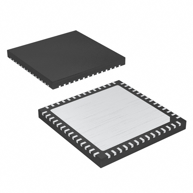
56-pin MLF
8x8mm body
IDTTM/ICSTM Embedded 56-Pin Industrial Temperature Range CK505 Compatible Clock
1
1612—08/19/09
�ICS9ERS3125
Embedded 56-Pin Industrial Temperature Range CK505 Compatible Clock
Datasheet
Pin Description
PIN #
1
X2
2
X1
3
VDDREF
PIN NAME
TYPE
OUT
IN
PWR
4
REF0/FSLC/TEST_SEL
I/O
5
6
SDATA
SCLK
I/O
IN
7
PCI0/CR#_A
I/O
8
VDDPCI
9
PCI1/CR#_B
I/O
10
PCI2/TME
I/O
11
PCI3
12
PCI4/27_SEL
I/O
13
PCI_F5/ITP_EN
I/O
14
15
GNDPCI
VDD48
PWR
OUT
PWR
PWR
16
USB_48MHz/FSLA
17
18
GND48
VDD96_IO
PWR
PWR
19
DOTT_96/SRCT0
OUT
20
DOTC_96/SRCC0
I/O
OUT
DESCRIPTION
Crystal output, nominally 14.318MHz.
Crystal input, Nominally 14.318MHz.
Power pin for the REF outputs, 3.3V nominal.
3.3V 14.318MHz reference clock/3.3V tolerant low threshold input for CPU frequency
selection. Refer to input electrical characteristics for Vil_FS and Vih_FS values/ TEST_SEL: 3level latched input to enable test mode. Refer to Test Clarification Table.
Data pin for SMBus circuitry, 5V tolerant.
Clock pin of SMBus circuitry, 5V tolerant.
3.3V PCI clock output or Clock Request control A for either SRC0 or SRC2 pair
The power-up default is PCI0 output, but this pin may also be used as a Clock Request
control of SRC pair 0 or SRC pair 2 via SMBus. Before configuring this pin as a Clock
Request Pin, the PCI output must first be disabled in byte 2, bit 0 of SMBus address space .
After the PCI output is disabled (high-Z), the pin can then be set to serve as a Clock Request
pin for either SRC pair 2 or pair 0 using the CR#_A_EN bit located in byte 5 of SMBUs
address space.
Byte 5, bit 7
0 = PCI0 enabled (default)
1= CR#_A enabled.
Byte 5, bit 6 controls whether CR#_A controls SRC0 or SRC2 pair
Byte 5, bit 6
0 = CR#_A controls SRC0 pair (default),
1= CR# A controls SRC2 pair
Power supply pin for the PCI outputs, 3.3V nominal
3.3V PCI clock output/Clock Request control B for either SRC1 or SRC4 pair
The power-up default is PCI1 output, but this pin may also be used as a Clock Request
control of SRC pair 1 or SRC pair 4 via SMBus. Before configuring this pin as a Clock
Request Pin, the PCI output must first be disabled in byte 2, bit 1 of SMBus address space .
After the PCI output is disabled (high-Z), the pin can then be set to serve as a Clock Request
pin for either SRC pair 1 or pair 4 using the CR#_B_EN bit located in byte 5 of SMBUs
address space.
Byte 5, bit 5
0 = PCI1 enabled (default)
1= CR#_B enabled.
Byte 5, bit 4 controls whether CR#_B controls SRC1 or SRC4 pair
Byte 5, bit 4
0 = CR#_B controls SRC1 pair (default)
1= CR# B controls SRC4 pair
3.3V PCI clock output / Trusted Mode Enable (TME) Latched Input. This pin is sampled on
power-up as follows
0 = Overclocking of CPU and SRC Allowed
1 = Overclocking of CPU and SRC NOT allowed
After being sampled on power-up, this pin becomes a 3.3V PCI Output
3.3V PCI clock output.
3.3V PCI clock output / 27MHz mode select for pin23, 24 strap. On powerup, the logic value
on this pin determines the power-up default of DOT_96/SRC0 and 27MHz/LCD/SRC1 output
and the function table for the pin23 and pin24.
Free running PCI clock output and ITP/SRC8 enable strap. This output is not affected by the
state of the PCI_STOP# pin. On powerup, the state of this pin determines whether pins 45
and 46 are an ITP or SRC pair.
0 =SRC8/SRC8#
1 = ITP/ITP#
Ground for PCI clocks.
Power supply for USB clock, nominal 3.3V.
Fixed 48MHz USB clock output. 3.3V./ 3.3V tolerant input for CPU frequency selection. Refer
to input electrical characteristics for Vil_FS and Vih_FS values.
Ground pin for the 48MHz outputs.
Power supply for DOT96 output. 1.05 to 3.3V +/-5%.
True clock of SRC or DOT96. The power-up default function is SRC0. After powerup, this pin
function may be changed to DOT96 via SMBus Byte 1, bit 7 as follows:
0= SRC0
1=DOT96
Complement clock of SRC or DOT96. The power-up default function is SRC0#. After
powerup, this pin function may be changed to DOT96# via SMBus Byte 1, bit 7 as follows
0= SRC0#
1=DOT96#
IDTTM/ICSTM Embedded 56-Pin Industrial Temperature Range CK505 Compatible Clock
2
1612—08/19/09
�ICS9ERS3125
Embedded 56-Pin Industrial Temperature Range CK505 Compatible Clock
Datasheet
Pin Description (continued)
21
22
GND
VDD
PWR
PWR
23
27FIX/LCDT/SRCT_LR1/SE1
OUT
24
27SS/LCDC/SRCC_LR1/SE2
OUT
25
26
27
28
29
GND
VDDPLL3_IO
SRCT2/SATAT
SRCC2/SATAC
GNDSRC
PWR
PWR
OUT
OUT
PWR
30
SRCT3/CR#_C
I/O
31
SRCC3/CR#_D
I/O
32
33
34
35
VDDSRC_IO
SRCT4
SRCC4
GNDSRC
36
SRCC11/CR#_G
PWR
I/O
I/O
PWR
I/O
Ground pin for the DOT96 clocks.
Power supply for SRC / SE1 and SE2 clocks, 3.3V nominal.
Single-ended 3.3V 27MHz fix clock output / True clock of differential SRC1 or LCD clock pair /
Single ended 3.3V peripheral clock output. The default output selection is determined by the
SEL_27 default latch value. See below:
27_SEL=0: LCD100 with -0.5% down spread is selected as default. LCD100 spread
percentage can be adjusted OR output can be changed to SRC or 3.3V single-ended
peripheral clock output via SMBUs B1b[4:1].
27_SEL=1: Single-ended 27FIX output is selected.
Single-ended 3.3V 27MHz fix clock output / Complementary clock of differential SRC1 or LCD
clock pair / Single ended 3.3V peripheral clock output. The default output selection is
determined by the SEL_27 default latch value. See below:
27_SEL=0: LCD100 with -0.5% down spread is selected as default. LCD100 spread
percentage can be adjusted OR output can be changed to SRC or 3.3V single-ended
peripheral clock output via SMBUs B1b[4:1].
27_SEL=1: Single-ended 27SS output is selected with -0.5% down spread as default.
Spread percentage can be adjusted via SMBus B1b[4:1].
Ground pin for SRC / SE1 and SE2 clocks, PLL3.
Power supply for PLL3 output. 1.05 to 3.3V +/-5%.
True clock of differential SRC/SATA clock pair.
Complement clock of differential SRC/SATA clock pair.
Ground pin for SRC clocks.
True clock of differential SRC clock pair/ Clock Request control C for either SRC0 or SRC2
pair
The power-up default is SRCCLK3 output, but this pin may also be used as a Clock Request
control of SRC pair 0 or SRC pair 2 via SMBus. Before configuring this pin as a Clock
Request Pin, the SRC3 output must first be disabled in byte 4, bit 7 of SMBus address space .
After the SRC3 output is disabled, the pin can then be set to serve as a Clock Request pin for
either SRC pair 2 or pair 0 using the CR#_C_EN bit located in byte 5 of SMBUs address
space.
Byte 5, bit 3
0 = SRC3 enabled (default)
1= CR#_C enabled.
Byte 5, bit 2 controls whether CR#_C controls SRC0 or SRC2 pair
Byte 5, bit 2
0 = CR#_C controls SRC0 pair (default),
1= CR# C controls SRC2 pair
Complementary clock of differential SRC clock pair/ Clock Request control D for either SRC1
or SRC4 pair
The power-up default is SRCCLK3 output, but this pin may also be used as a Clock Request
control of SRC pair 1 or SRC pair 4 via SMBus. Before configuring this pin as a Clock
Request Pin, the SRC3 output must first be disabled in byte 4, bit 7 of SMBus address space .
After the SRC3 output is disabled, the pin can then be set to serve as a Clock Request pin for
either SRC pair 1 or pair 4 using the CR#_D_EN bit located in byte 5 of SMBUs address
space.
Byte 5, bit 1
0 = SRC3 enabled (default)
1= CR#_D enabled.
Byte 5, bit 0 controls whether CR#_D controls SRC1 or SRC4 pair
Byte 5, bit 0
0 = CR#_D controls SRC1 pair (default),
1= CR# D controls SRC4 pair
Power supply for SRC clocks. 1.05 to 3.3V +/-5%.
True clock of differential SRC clock pair 4
Complement clock of differential SRC clock pair 4
Ground for SRC clocks
SRC11 complement /Clock Request control for SRC10 pair
The power-up default is SRC11#, but this pin may also be used as a Clock Request control of
SRC10 via SMBus. Before configuring this pin as a Clock Request Pin, the SRC11 output pair
must first be disabled in byte 3, bit 7 of SMBus configuration space After the SRC11 output is
disabled (high-Z), the pin can then be set to serve as a Clock Request for SRC10 pair using
byte 6, bit 5 of SMBus configuration space
Byte 6, bit 5
0 = SRC11# enabled (default)
1= CR#_G controls SRC10
NOTE: SRC10 NOT AVAILABLE ON 9LRS3125
IDTTM/ICSTM Embedded 56-Pin Industrial Temperature Range CK505 Compatible Clock
3
1612—08/19/09
�ICS9ERS3125
Embedded 56-Pin Industrial Temperature Range CK505 Compatible Clock
Datasheet
Pin Description (continued)
37
SRCT11/CR#_H
I/O
38
VDDSRC_IO
PWR
39
CPU_STOP#
IN
40
PCI_STOP#
IN
41
42
VDDSRC
GNDSRC
43
SRCC7CR#_E
I/O
44
SRCT7/CR#_F
I/O
45
CPUC2_ITP/SRCC8
OUT
46
CPUT2_ITP/SRCT8
OUT
47
VDDCPUI/O
PWR
48
CPUC1_F
OUT
PWR
PWR
49
CPUT1_F
OUT
50
51
52
53
54
GNDCPU
CPUC0
CPUT0
VDDCPU
CK_PWRGD/PD#
PWR
OUT
OUT
PWR
IN
55
FSLB/TEST_MODE
56
GNDREF
IN
PWR
SRC11 true or Clock Request control H for SRC11 pair
The power-up default is SRC11, but this pin may also be used as a Clock Request control of
SRC3 via SMBus. Before configuring this pin as a Clock Request Pin, the SRC11 output pair
must first be disabled in byte 3, bit 7 of SMBus configuration space After the SRC11 output is
disabled (high-Z), the pin can then be set to serve as a Clock Request for SRC3 pair using
byte 6, bit 4 of SMBus configuration space
Byte 6, bit 4
0 = SRC11 enabled (default)
1= CR#_H controls SRC3.
NOTE: SRC10 NOT AVAILABLE ON 9LRS3125
Power supply for SRC outputs. 1.05 to 3.3V +/-5%.
Stops all CPU Clocks, except those set to be free running clocks.
In AMT mode 3 bits are shifted in from the ICH to set the FSC, FSB, FSA values
Stops all PCI/SRC Clocks, except those set to be free running clocks.
In AMT mode, this pin is a clock input which times the FSC, FSB, FSA bits shifted in on
CPU_STOP#..
3.3V Power supply for SRC PLL and Logic
Ground for SRC clocks
SRC7 complement or Clock Request control E for SRC6 pair
The power-up default is SRC7#, but this pin may also be used as a Clock Request control of
SRC6 via SMBus. Before configuring this pin as a Clock Request Pin, the SRC7 output pair
must first be disabled in byte 3, bit 3 of SMBus configuration space . After the SRC output is
disabled (high-Z), the pin can then be set to serve as a Clock Request for SRC6 pair using
byte 6, bit 7 of SMBus configuration space
Byte 6, bit 7
0 = SRC7# enabled (default)
1= CR# E controls SRC6.
SRC7 true or Clock Request control 8 for SRC8 pair
The power-up default is SRC7, but this pin may also be used as a Clock Request control of
SRC8 via SMBus. Before configuring this pin as a Clock Request Pin, the SRC7 output pair
must first be disabled in byte 3, bit 3 of SMBus configuration space After the SRC output is
disabled (high-Z), the pin can then be set to serve as a Clock Request for SRC8 pair using
byte 6, bit 6 of SMBus configuration space
Byte 6, bit 6
0 = SRC7# enabled (default)
1 = CR# F controls SRC8.
Complement clock of low power differential CPU2/Complement clock of differential SRC pair.
The function of this pin is determined by the latched input value on pin 14, PCIF5/ITP_EN on
powerup. The function is as follows:
Pin 14 latched input Value
0 = SRC8#
1 = ITP#
True clock of low power differential CPU2/True clock of differential SRC pair. The function of
this pin is determined by the latched input value on pin 14, PCIF5/ITP_EN on powerup. The
function is as follows:
Pin 14 latched input Value
0 = SRC8
1 = ITP
Power supply for CPU outputs. 1.05 to 3.3V +/-5%.
Complement clock of low power differential CPU clock pair. This clock will be free-running
during iAMT.
True clock of low power differential CPU clock pair. This clock will be free-running during
iAMT.
Ground Pin for CPU Outputs
Complement clock of low power differential CPU clock pair.
True clock of low power differential CPU clock pair.
3.3V Power Supply for CPU.
Notifies CK505 to sample latched inputs, or iAMT entry/exit, or PWRDWN# mode
3.3V tolerant input for CPU frequency selection. Refer to input electrical characteristics for
Vil_FS and Vih_FS values. TEST_MODE is a real time input to select between Hi-Z and
REF/N divider mode while in test mode. Refer to Test Clarification Table.
Ground pin for crystal oscillator circuit
IDTTM/ICSTM Embedded 56-Pin Industrial Temperature Range CK505 Compatible Clock
4
1612—08/19/09
�ICS9ERS3125
Embedded 56-Pin Industrial Temperature Range CK505 Compatible Clock
Datasheet
General Description
ICS9ERS3125 is electrically compliant to the Intel CK505 Yellow Cover specification. This clock synthesizer provides a single chip
solution for Intel chipsets. ICS9ERS3125 is driven with a 14.318MHz crystal.
Block Diagram
Xtal
REFCLK
SS
PLL1
SE1
1
27SS - SE2
LCD
SRC1
27SS, SE1, SE2, LCD/SRC1
0
COUT_DIV
27_SEL
SS
PLL2
PCI
1
PCICLK
0
SS
PLL5
COUT_DIV
1
B1bit0
SRC_M ain
SRC(11),(7:6),(4:3)
0
P CICLK
B0bit2
CP UCLK
CPUCLK(1:0)
0
COUT_DIV
SRC8
Fix
PLL3
SATA
ITP_EN
SRC
SA TA
COUT_DIV
SRC8/CPU2_ITP
1
0
SRC2/SATA
1
B0
48MHz
48MHz
SRC0
DOT_96
0
SRC0/ DOT96M
1
B1b7
27FIX
Power Groups
Pin Number
VDD
GND
47
50
53
50
26, 32, 38
29, 35, 42
41
42
26
25
22
25
18
21
15
17
3
56
8
14
Description
CPUCLK
Low power outputs
Master Clock, Analog
Low power outputs
SRCCLK
PLL2
Low power outputs
PLL1/SE
PLL1
DOT 96Mhz
Low power outputs
USB 48 output and PLL
Xtal, REF
PCICLK
IDTTM/ICSTM Embedded 56-Pin Industrial Temperature Range CK505 Compatible Clock
5
1612—08/19/09
�ICS9ERS3125
Embedded 56-Pin Industrial Temperature Range CK505 Compatible Clock
Datasheet
Absolute Maximum Ratings
PARAMETER
SYMBOL
CONDITIONS
Maximum Supply Voltage
VDDxxx
Supply Voltage
Maximum Supply Voltage
VDDxxx_IO
Low-Voltage Differential I/O Supply
3.8
V
1,7
Maximum Input Voltage
VIH
3.3V LVCMOS Inputs
4.6
V
1,7,8
Minimum Input Voltage
VIL
Any Input
GND - 0.5
V
1,7
Storage Temperature
Ts
-
-65
150
°
1,7
115
°C
1
Human Body Model
2000
V
1,7
Case Temperature
Tcase
Input ESD protection
ESD prot
MIN
MAX
UNITS
Notes
4.6
V
1,7
C
Electrical Characteristics - Input/Supply/Common Output Parameters
PARAMETER
SYMBOL
CONDITIONS
MIN
MAX
UNITS
Ambient Operating Temp
Tambient
-
-40
85
°C
1
Supply Voltage
VDDxxx
Supply Voltage
3.135
3.465
V
1
Supply Voltage
VDDxxx_IO
Low-Voltage Differential I/O Supply
1
3.465
V
1
Input High Voltage
VIHSE
Single-ended inputs
2
VDD + 0.3
V
1
Input Low Voltage
VILSE
Single-ended inputs
VSS - 0.3
0.8
V
1
Input Leakage Current
IIN
-5
5
uA
1
Input Leakage Current
IINRES
VIN = VDD , VIN = GND
Inputs with pull or pull down
resistors
VIN = VDD , VIN = GND
-200
200
uA
1
Output High Voltage
VOHSE
Single-ended outputs, IOH = -1mA
V
1
Output Low Voltage
VOLSE
Single-ended outputs, IOL = 1 mA
Output High Voltage
VOHDIF
Differential Outputs
Output Low Voltage
Low Threshold InputHigh Voltage (Test Mode)
Low Threshold InputHigh Voltage
Low Threshold InputLow Voltage
VOLDIF
Differential Outputs
VIH_FS_TEST
3.3 V +/-5%
VIH_FS
V
1
0.9
V
1
0.4
V
1
2
VDD + 0.3
V
1
3.3 V +/-5%
0.7
1.5
V
1
VIL_FS
3.3 V +/-5%
VSS - 0.3
0.35
V
1
IDD_DEFAULT
95
125
mA
1
106
125
mA
1
101
125
mA
1
32
50
mA
1
IDD_PD3.3
3.3V supply, PLL1,2 off
3.3V supply, PLL1,2 Differential
Out
3.3V supply, PLL1,2 Single-ended
Out
0.8V supply, Differential IO current,
all outputs enabled
3.3V supply, Power Down Mode
26
30
mA
1
IDD_PDIO
0.8V IO supply, Power Down Mode
0.23
0.5
mA
1
IDD_PLL3SE
IDD_IO
Power Down Current
2.4
Notes
0.4
IDD_PLL3DIF
Operating Supply Current
TYPICAL
0.7
25
IDD_iAMT3.3
3.3V supply, iAMT Mode
47
60
mA
1
IDD_iAMT0.8
0.8V IO supply, iAMTMode
5
10
mA
1
Input Frequency
Fi
VDD = 3.3 V
14.318
MHz
2
Pin Inductance
Lpin
1
iAMT Mode Current
Input Capacitance
Spread Spectrum Modulation
Frequency
7
nH
5
pF
1
Output pin capacitance
6
pF
1
CINX
X1 & X2 pins
5
pF
1
fSSMOD
Triangular Modulation
33
kHz
1
CIN
Logic Inputs
COUT
1.5
IDTTM/ICSTM Embedded 56-Pin Industrial Temperature Range CK505 Compatible Clock
6
30
1612—08/19/09
�ICS9ERS3125
Embedded 56-Pin Industrial Temperature Range CK505 Compatible Clock
Datasheet
Electrical Characteristics - SMBus Interface
PARAMETER
SYMBOL
SMBus Voltage
VDD
CONDITIONS
Low-level Output Voltage
Current sinking at
VOLSMB = 0.4 V
SCLK/SDATA
Clock/Data Rise Time
SCLK/SDATA
Clock/Data Fall Time
Maximum SMBus Operating
Frequency
VOLSMB
@ IPULLUP
IPULLUP
SMB Data Pin
TFI2C
(Max VIL - 0.15) to
(Min VIH + 0.15)
(Min VIH + 0.15) to
(Max VIL - 0.15)
FSMBUS
Block Mode
TRI2C
MIN
MAX
UNITS
Notes
2.7
5.5
V
1
0.4
V
1
mA
1
1000
ns
1
300
ns
1
100
kHz
1
MAX
UNITS
Notes
1.8
ms
1
15
ns
1
300
us
1
10
ns
1
5
ns
1
5
ns
1
4
AC Electrical Characteristics - Input/Common Parameters
PARAMETER
SYMBOL
Clk Stabilization
TSTAB
Tdrive_SRC
TDRSRC
Tdrive_PD#
TDRPD
Tdrive_CPU
TDRSRC
Tfall_PD#
TFALL
Trise_PD#
TRISE
CONDITIONS
From VDD Power-Up or deassertion of PD# to 1st clock
SRC output enable after
PCI_STOP# de-assertion
Differential output enable after
PD# de-assertion
CPU output enable after
CPU_STOP# de-assertion
MIN
Fall/rise time of PD#, PCI_STOP#
and CPU_STOP# inputs
AC Electrical Characteristics - Low Power Differential Outputs
PARAMETER
SYMBOL
CONDITIONS
MIN
MAX
UNITS
NOTES
Rising Edge Slew Rate
tSLR
Differential Measurement
2.5
8
V/ns
1,2
Falling Edge Slew Rate
tFLR
Differential Measurement
2.5
8
V/ns
1,2
Slew Rate Variation
tSLVAR
Single-ended Measurement
20
%
1
Maximum Output Voltage
VHIGH
Includes overshoot
1150
mV
1
Minimum Output Voltage
VLOW
Includes undershoot
-300
mV
1
Differential Voltage Swing
VSWING
Differential Measurement
300
mV
1
Crossing Point Voltage
VXABS
Single-ended Measurement
300
550
mV
1,3,4
Crossing Point Variation
VXABSVAR
Single-ended Measurement
140
mV
1,3,5
Duty Cycle
DCYC
Differential Measurement
55
%
1
CPU Jitter - Cycle to Cycle
CPUJ C2C
Differential Measurement
85
ps
1
SRC Jitter - Cycle to Cycle
SRCJ C2C
Differential Measurement
125
ps
1
SATA Jitter - Cycle to Cycle
SATAJ C2C
Differential Measurement
125
ps
1
DOT Jitter - Cycle to Cycle
DOTJ C2C
Differential Measurement
250
ps
1
CPU[1:0] Skew
CPUSKEW10
Differential Measurement
100
ps
1
CPU[2_ITP:0] Skew
CPUSKEW20
Differential Measurement
150
ps
1
SRC[11,7,4,2,0] Skew
SRCSKEW
Differential Measurement
SRC[11:0] Skew
SRCSKEW
Differential Measurement
45
0 nominal
3
ps
1
ns
1
*TA = -40 - 85°C; Supply Voltage VDD = 3.3 V +/-5%, Rs= 0Ω, CL = 2pF
IDTTM/ICSTM Embedded 56-Pin Industrial Temperature Range CK505 Compatible Clock
7
1612—08/19/09
�ICS9ERS3125
Embedded 56-Pin Industrial Temperature Range CK505 Compatible Clock
Datasheet
Electrical Characteristics - PCICLK/PCICLK_F
PARAMETER
SYMBOL
CONDITIONS
MIN
MAX
UNITS
NOTES
Long Accuracy
ppm
see Tperiod min-max values
-100
100
ppm
1,6
Clock period
Tperiod
30.50300
ns
6
30.15320
ns
6
Absolute min/max period
Tabs
33.33MHz output nominal/spread
29.49718
30.65320
ns
6
Output High Voltage
VOH
IOH = -1 mA
2.4
V
1
Output Low Voltage
VOL
IOL = 1 mA
0.4
V
1
Output High Current
IOH
mA
1
Output Low Current
IOL
33.33MHz output nominal
33.33MHz output spread
29.99718
V OH @MIN = 1.0 V
-33
VOH@MAX = 3.135 V
-33
VOL @ MIN = 1.95 V
mA
1
mA
1
38
mA
1
30
VOL @ MAX = 0.4 V
Rising Edge Slew Rate
tSLR
Measured from 0.8 to 2.0 V
1
4
V/ns
1
Falling Edge Slew Rate
tFLR
Measured from 2.0 to 0.8 V
1
4
V/ns
1
Duty Cycle
dt1
VT = 1.5 V
45
55
%
1
Skew
tskew
VT = 1.5 V
250
ps
1
Intentional PCI-PCI delay
tdelay
VT = 1.5 V
ps
1,9
Jitter, Cycle to cycle
tjcyc-cyc
VT = 1.5 V
ps
1
200 nominal
500
*TA = -40 - 85°C; Supply Voltage VDD = 3.3 V +/-5%, Rs = 39Ω, CL = 5pF
Electrical Characteristics - USB48MHz
PARAMETER
Long Accuracy
SYMBOL
ppm
CONDITIONS
see Tperiod min-max values
MIN
-100
MAX
100
UNITS
ppm
NOTES
Clock period
Tperiod
48.00MHz output nominal
20.83125
20.83542
ns
6
Absolute min/max period
Tabs
48.00MHz output nominal
20.13125
21.53542
ns
6
Output High Voltage
VOH
IOH = -1 mA
2.4
V
1
Output Low Voltage
VOL
Output High Current
IOH
IOL = 1 mA
0.4
V OH @MIN = 1.0 V
-29
VOH@MAX = 3.135 V
-23
VOL @ MIN = 1.95 V
29
1,6
V
1
mA
1
mA
1
mA
1
27
mA
1
2
V/ns
1
Output Low Current
IOL
Rising Edge Slew Rate
tSLR
Measured from 0.8 to 2.0 V
Falling Edge Slew Rate
tFLR
Measured from 2.0 to 0.8 V
1
2
V/ns
1
Duty Cycle
dt1
VT = 1.5 V
45
55
%
1
Jitter, Cycle to cycle
tjcyc-cyc
VT = 1.5 V
350
ps
1
VOL @ MAX = 0.4 V
1
*TA = -40 - 85°C; Supply Voltage VDD = 3.3 V +/-5%, Rs = 39Ω, CL = 5pF
Electrical Characteristics - REF-14.318MHz
PARAMETER
SYMBOL
CONDITIONS
MIN
MAX
UNITS
Notes
Long Accuracy
ppm
see Tperiod min-max values
-100
100
ppm
1,6
Clock period
Tperiod
14.318MHz output nominal
69.8343
69.8483
ns
6
Absolute min/max period
Tabs
14.318MHz output nominal
68.8343
70.84825
ns
6
Output High Voltage
VOH
IOH = -1 mA
2.4
Output Low Voltage
VOL
IOL = 1 mA
Output High Current
IOH
Output Low Current
IOL
Rising Edge Slew Rate
tSLR
Measured from 0.8 to 2.0 V
Falling Edge Slew Rate
tFLR
Measured from 2.0 to 0.8 V
Duty Cycle
dt1
VT = 1.5 V
Jitter
tjcyc-cyc
VT = 1.5 V
VOH @MIN = 1.0 V,
VOH@MAX = 3.135 V
VOL @MIN = 1.95 V,
VOL @MAX = 0.4 V
V
1
0.4
V
1
-33
-33
mA
1
30
38
mA
1
1
4
V/ns
1
1
4
V/ns
1
45
55
%
1
1000
ps
1
*TA = -40 - 85°C; Supply Voltage VDD = 3.3 V +/-5%, Rs = 39Ω, CL = 5pF
IDTTM/ICSTM Embedded 56-Pin Industrial Temperature Range CK505 Compatible Clock
8
1612—08/19/09
�ICS9ERS3125
Embedded 56-Pin Industrial Temperature Range CK505 Compatible Clock
Datasheet
Electrical Characteristics - 27MHz_Spread / 27MHz_NonSpread
PARAMETER
SYMBOL
CONDITIONS
MIN
MAX
UNITS
Notes
Long Accuracy
ppm
see Tperiod min-max values
-50
50
ppm
1,6
Clock period
T period
27.000MHz output nominal
37.0352
37.0389
ns
6
Output High Voltage
VOH
IOH = -1 mA
2.4
V
1
Output Low Voltage
VOL
V
1
mA
1
Output High Current
IOH
IOL = 1 mA
0.55
V OH @MIN = 1.0 V
-29
VOH@MAX = 3.135 V
-23
VOL @ MIN = 1.95 V
29
mA
1
mA
1
Output Low Current
IOL
27
mA
1
Edge Rate
tslewr/f
Rising/Falling edge rate
1
4
V/ns
1
Rise Time
tr1
VOL = 0.4 V, VOH = 2.4 V
0.5
2
ns
1
Fall Time
tf1
VOH = 2.4 V, VOL = 0.4 V
0.5
2
ns
1
Duty Cycle
dt1
VT = 1.5 V
45
55
%
1
tltj
Long Term (10us), VT = 1.5 V
800
ps
1
tjpk-pk
VT = 1.5 V
tjcyc-cyc
VT = 1.5 V
Jitter
VOL @ MAX = 0.4 V
-200
200
ps
1
200
ps
1
Max
Units
Notes
86
ps (p-p)
ps
(RMS)
ps
(RMS)
1,11
*TA = -40 - 85°C; Supply Voltage VDD = 3.3 V +/-5%, Rs = 39Ω, CL = 5pF
Electrical Characteristics - Differential Jitter Parameters
PARAMETER
Symbol
Conditions
Min
tjphasePLL
PCIe Gen 1
PCIe Gen 2
tjphaseLo
Jitter, Phase
10kHz < f < 1.5MHz
PCIe Gen 2
tjphaseHigh
1.5MHz < f < Nyquist (50MHz)
*TA = -40 - 85°C; Supply Voltage VDD = 3.3 V +/-5%, Rs= 0Ω, CL = 2pF
TYP
3
3.1
1,11
1,11
Notes on Electrical Characteristics:
1
Guaranteed by design and characterization, not 100% tested in production.
2
Slew rate measured through Vswing centered around differential zero
3
Vxabs is defined as the voltage where CLK = CLK#
4
Only applies to the differential rising edge (CLK rising and CLK# falling)
Defined as the total variation of all crossing voltages of CLK rising and CLK# falling. Matching applies to rising edge rate of CLK
and falling edge of CLK#. It is measured using a +/-75mV window centered on the average cross point where CLK meets CLK#.
The average cross point is used to calculate the voltage thresholds the oscilloscope is to use for the edge rate calculations.
6
All Long Term Accuracy and Clock Period specifications are guaranteed assuming that REFOUT is at 14.31818MHz
5
7
Operation under these conditions is neither implied, nor guaranteed.
8
Maximum input voltage is not to exceed maximum VDD
9
See PCI Clock-to-Clock Delay Figure
10
At nominal voltage and temperature
11
See http://www.pcisig.com for complete specs
IDTTM/ICSTM Embedded 56-Pin Industrial Temperature Range CK505 Compatible Clock
9
1612—08/19/09
�ICS9ERS3125
Embedded 56-Pin Industrial Temperature Range CK505 Compatible Clock
Datasheet
Table 1: CPU Frequency Select Table
2
FSLC
B0b7
0
0
0
0
1
1
1
1
1
FSLB
B0b6
0
0
1
1
0
0
1
1
1
FSLA
B0b5
0
1
0
1
0
1
0
1
CPU
MHz
SRC
MHz
PCI
MHz
REF
MHz
USB
MHz
DOT
MHz
266.66
133.33
200.00
166.66
333.33
100.00
400.00
100.00
33.33
14.318
48.00
96.00
Reserved
1. FSLA and FSLB are low-threshold inputs.Please see VIL_FS and VIH_FS specifications in
the Input/Supply/Common Output Parameters Table for correct values.
Also refer to the Test Clarification Table.
2. FSLC is a three-level input. Please see the VIL_FS and VIH_FS
specifications in the Input/Supply/Common Output Parameters Table for correct values.
Table 2: 27FIX/LCDT/SRCT_LR1/SE1, 27SS/LCDC/SRCC_LR1/SE2 Configuration
27FIX/LCDT/SRCT_LR1/SE1 27SS/LCDC/SRCC_LR1/SE2
B1b3
B1b2
B1b1
27_SEL B1b4
Spread
MHz
%
PLL1 & PLL2 disabled
100.00
100.00
-0.50%
100.00
-1%
100.00
-1.50%
100.00
+/-0.25%
100.00
+/-0.5%
N/A
N/A
24.576
None
98.304
None
98.304
None
27.000
None
25.000
None
MHz
0
0
0
0
0
0
0
0
1
100.00
0
0
0
1
0
100.00
0
0
0
1
1
100.00
0
0
1
0
0
100.00
0
0
1
0
1
100.00
0
0
1
1
0
100.00
0
0
1
1
1
N/A
0
1
0
0
0
24.576
0
1
0
0
1
24.576
0
1
0
1
0
98.304
0
1
0
1
1
27.000
0
1
1
0
0
25.000
0
1
1
0
1
0
1
1
1
0
N/A
N/A
0
1
1
1
1
N/A
N/A
0
0
0
0
0
N/A
N/A
1
0
0
0
1
N/A
N/A
1
27MHz_nonSS
0
0
1
0
27MHz_SS
1
27MHz_nonSS
0
0
1
1
1
27MHz_SS
27MHz_nonSS
0
1
0
0
27MHz_SS
1
27MHz_nonSS
0
1
0
1
27MHz_SS
1
27MHz_nonSS
0
1
1
0
27MHz_SS
1
27MHz_nonSS
0
1
1
1
27MHz_SS
1
27MHz_nonSS
1
0
0
0
27MHz_SS
1
27MHz_nonSS
1
0
0
1
1
27MHz_SS
27MHz_nonSS
1
0
1
0
27MHz_SS
1
1
0
1
1
N/A
N/A
1
1
1
0
0
N/A
N/A
1
1
1
0
1
N/A
N/A
1
1
1
1
0
N/A
N/A
1
1
1
1
1
1
N/A
N/A
Note: Mode 00000 ~ 00110 on Table 2 only applies when SRC_MAIN source is from PLL5.
IDTTM/ICSTM Embedded 56-Pin Industrial Temperature Range CK505 Compatible Clock
10
N/A
N/A
N/A
N/A
Comment
SRCCLK1 from SRC_MAIN
LCDCLK from PLL1
LCDCLK from PLL1
LCDCLK from PLL1
LCDCLK from PLL1
LCDCLK from PLL1
N/A
24.576Mhz on SE1 and SE2
24.576Mhz on SE1, 98.304Mhz on SE2
98.304Mhz on SE1 and SE2
27Mhz on SE1 and SE2
25Mhz on SE1 and SE2
N/A
N/A
N/A
-0.5%
-1%
-1.5%
-2%
-0.75%
-1.25%
-1.75%
+-0.5%
+-0.75%
1612—08/19/09
�ICS9ERS3125
Embedded 56-Pin Industrial Temperature Range CK505 Compatible Clock
Datasheet
Table 3: IO_Vout select table
B9b2
0
0
0
0
1
1
1
1
B9b1
0
0
1
1
0
0
1
1
B9b0
0
1
0
1
0
1
0
1
IO_Vout
0.3V
0.4V
0.5V
0.6V
0.7V
0.8V
0.9V
1.0V
Table 4: Device ID table
B8b7
B8b6
B8b5
B8b4
Comment
0
0
0
0
0
0
0
0
1
1
1
1
1
1
1
0
0
0
0
1
1
1
1
1
1
1
1
1
1
1
0
0
1
1
0
0
1
1
0
0
1
1
0
0
1
0
1
0
1
0
1
0
1
0
1
0
1
0
1
0
9LRS3125BIK
1
1
1
1
Reserved
Reserved
Reserved
Reserved
Reserved
Reserved
Reserved
Reserved
Reserved
Reserved
Reserved
Reserved
Reserved
Reserved
Reserved
IDTTM/ICSTM Embedded 56-Pin Industrial Temperature Range CK505 Compatible Clock
11
1612—08/19/09
�ICS9ERS3125
Embedded 56-Pin Industrial Temperature Range CK505 Compatible Clock
Datasheet
CPU Power Management Table
PD#
CPU_STOP# PCI_STOP# PEREQ#
1
0
1
1
1
X
0
X
1
X
X
X
M1
X
X
X
X
SMBus
Register
OE
Enable
Enable
Enable
Disable
CPU0
CPU0#
Running
Low/20K
High
Low/20K
Low/20K
Running
Low
Low
Low
Low
CPU1
CPU1#
CPU2
CPU2#
Running Running Running Running
Low/20K Low Low/20K
Low
High
Low
High
Low
Low/20K Low Low/20K
Low
Running Running Low/20K
Low
PCIEX, LCD Power Management Table
PD#
1
0
1
1
1
CPU_STOP# PCI_STOP# PEREQ#
X
X
X
X
X
1
X
0
X
X
M1
0
X
0
1
X
SMBus
Register
OE
Enable
Enable
Enable
Enable
Disable
PCIeT
PCIeC
Free-Run
Running
Running
Low/20K
Low
Running
Running
Running
Running
Low/20K
Low
Low/20K
Low
PCIeT
PCIeC
Stoppable
Running Running
Low/20K
Low
High
Low
Low/20K
Low
Low/20K
Low
Low/20K
Low
LCD
LCD #
Free-Run
Running Running
Low/20K
Low
Running Running
Running Running
Low/20K
Low
Low/20K
Low
LCD
LCD #
Stoppable
Running Running
Low/20K
Low
High
Low
Running Running
Low/20K
Low
Low/20K
Low
SATA
SATA#
Free-Run
Running Running
Low/20K
Low
Running Running
Running Running
Low/20K
Low
Low/20K
Low
SATA
SATA#
Stoppable
Running Running
Low/20K
Low
High
Low
Running Running
Low/20K
Low
Low/20K
Low
DOT Power Management Table
PD#
1
0
1
1
1
CPU_STOP# PCI_STOP# PEREQ#
X
X
X
X
X
1
X
0
X
X
M1
X
X
X
X
X
SMBus
Register
OE
Enable
Enable
Enable
Enable
Disable
DOT
DOT#
Running
Low/20K
Running
Running
Low/20K
Low/20K
Running
Low
Running
Running
Low
Low
Singled-Ended Power Management Table
PD#
1
0
1
1
CPU_STOP# PCI_STOP# PEREQ#
X
X
X
X
1
X
0
X
M1
X
X
X
X
SMBus
Register
OE
Enable
Enable
Enable
Disable
PCIF/PCI PCIF/PCI
Free-Run Stoppable
Running
Low
Running
Low
Low
IDTTM/ICSTM Embedded 56-Pin Industrial Temperature Range CK505 Compatible Clock
12
Running
Low
Low
Low
Low
USB48
REF
27M
SE
Running Running Running Running
Low
Low
Low
Low
Running Running Running Running
Low
Low
Low
Low
Low
Low
Low
Low
1612—08/19/09
�ICS9ERS3125
Embedded 56-Pin Industrial Temperature Range CK505 Compatible Clock
Datasheet
Differential Clock Tolerances
PPM tolerance
Cycle to Cycle Jitter
Spread
CPU
100
50
-0.50%
SRC
100
125
-0.50%
DOT96
100
250
0
BMC133
100
125
-0.50%
ppm
ps
%
Clock Periods - Differential Outputs with Spread Spectrum Disabled
SSC OFF
CPU
SRC
DOT96
Center
Freq.
MHz
100.00
133.33
166.67
200.00
266.67
333.33
400.00
100.00
96.00
Measurement Window
1us
0.1s
0.1s
0.1s
+ ppm
-SSC
- ppm
0 ppm
-c2c jitter
Long-Term
Short-Term Long-Term
Period
AbsPer
Average
Average
Average
Nominal
Min
Max
Min
Min
9.94900
9.99900
10.00000
10.00100
7.44925
7.49925
7.50000
7.50075
5.94940
5.99940
6.00000
6.00060
4.94950
4.99950
5.00000
5.00050
3.69962
3.74962
3.75000
3.75037
2.94970
2.99970
3.00000
3.00030
2.44975
2.49975
2.50000
2.50025
9.87400
9.99900
10.00000
10.00100
10.16563
10.41563
10.41667
10.41771
1 Clock
1us
+SSC
Short-Term
Average
Max
1 Clock
Units Notes
+c2c jitter
10.05100
7.55075
6.05060
5.05050
3.80037
3.05030
2.55025
10.12600
10.66771
ns
ns
ns
ns
ns
ns
ns
ns
ns
1,2
1,2
1,2
1,2
1,2
1,2
1,2
1,2
1,2
Clock Periods - Differential Outputs with Spread Spectrum Enabled
SSC ON
CPU
SRC
1
2
Center
Freq.
MHz
99.75
133.00
166.25
199.50
266.00
332.50
399.00
99.75
Measurement Window
1us
0.1s
0.1s
0.1s
-SSC
- ppm
+ ppm
-c2c jitter
0 ppm
Short-Term Long-Term
Long-Term
AbsPer
Period
Average
Average
Average
Min
Nominal
Min
Min
Max
9.94906
9.99906
10.02406
10.02506
10.02607
7.44930
7.49930
7.51805
7.51880
7.51955
5.94944
5.99944
6.01444
6.01504
6.01564
4.94953
4.99953
5.01203
5.01253
5.01303
3.69965
3.74965
3.75902
3.75940
3.75977
2.94972
2.99972
3.00722
3.00752
3.00782
2.44977
2.49977
2.50602
2.50627
2.50652
9.87406
9.99906
10.02406
10.02506
10.02607
1 Clock
1us
+SSC
Short-Term
Average
Max
10.05107
7.53830
6.03064
5.02553
3.76915
3.01532
2.51277
10.05107
1 Clock
Units Notes
+c2c jitter
10.10107
7.58830
6.08064
5.07553
3.81915
3.06532
2.56277
10.17607
ns
ns
ns
ns
ns
ns
ns
ns
1,2
1,2
1,2
1,2
1,2
1,2
1,2
1,2
Guaranteed by design and characterization, not 100% tested in production.
All Long Term Accuracy specifications are guaranteed with the assumption that the crystal input is tuned to exactly 14.31818MHz.
IDTTM/ICSTM Embedded 56-Pin Industrial Temperature Range CK505 Compatible Clock
13
1612—08/19/09
�ICS9ERS3125
Embedded 56-Pin Industrial Temperature Range CK505 Compatible Clock
Datasheet
General SMBus serial interface information for the ICS9ERS3125
How to Write:
How to Read:
Controller (host) sends a start bit.
Controller (host) sends the write address D2 (H)
ICS clock will acknowledge
Controller (host) sends the beginning byte location = N
ICS clock will acknowledge
Controller (host) sends the data byte count = X
ICS clock will acknowledge
Controller (host) starts sending Byte N through
Byte N + X -1
• ICS clock will acknowledge each byte one at a time
• Controller (host) sends a Stop bit
•
•
•
•
•
•
•
•
•
•
•
•
•
•
•
•
•
•
•
•
•
•
Controller (host) will send start bit.
Controller (host) sends the write address D2 (H)
ICS clock will acknowledge
Controller (host) sends the begining byte
location = N
ICS clock will acknowledge
Controller (host) will send a separate start bit.
Controller (host) sends the read address D3 (H)
ICS clock will acknowledge
ICS clock will send the data byte count = X
ICS clock sends Byte N + X -1
ICS clock sends Byte 0 through byte X (if X(H)
was written to byte 8).
Controller (host) will need to acknowledge each byte
Controller (host) will send a not acknowledge bit
Controller (host) will send a stop bit
Index Block Write Operation
Controller (Host)
starT bit
T
Slave Address D2(H)
WR
WRite
Index Block Read Operation
Controller (Host)
T
starT bit
Slave Address D2(H)
WR
WRite
ICS (Slave/Receiver)
ICS (Slave/Receiver)
ACK
ACK
Beginning Byte = N
Beginning Byte = N
ACK
ACK
RT
Repeat starT
Slave Address D3(H)
RD
ReaD
Data Byte Count = X
ACK
Beginning Byte N
ACK
X Byte
ACK
Data Byte Count = X
ACK
Beginning Byte N
Byte N + X - 1
ACK
X Byte
ACK
P
stoP bit
Byte N + X - 1
N
P
IDTTM/ICSTM Embedded 56-Pin Industrial Temperature Range CK505 Compatible Clock
14
Not acknowledge
stoP bit
1612—08/19/09
�ICS9ERS3125
Embedded 56-Pin Industrial Temperature Range CK505 Compatible Clock
Datasheet
Byte 0 FS Readback & PLL Selection Register
Bit
7
6
5
Name
FSLC
FSLB
FSLA
Description
CPU Freq. Sel. Bit (Most Significant)
CPU Freq. Sel. Bit
CPU Freq. Sel. Bit (Least Significant)
Type
R
R
R
4
iAMT_EN
Set via SMBus or dynamically by CK505 if detects dynamic M1
R
3
2
1
SRC_Main_SEL
SATA_SEL
0
PD_Restore
Reserved
Select source for SRC Main
RW
Select source for SATA clock
RW
1 = on Power Down de-assert return to last known state
0 = clear all SMBus configurations as if cold power-on and go to
RW
latches open state
This bit is ignored and treated at '1' if device is in iAMT mode.
0
1
Legacy Mode
iAMT Enabled
SRC Main = PLL5
SATA = SRC_Main
SRC Main = PLL2
SATA = PLL3
Default
Latch
Latch
Latch
iAMT power
on status
1
0
0
Configuration Not
Saved
Configuration Saved
1
See Table 1 : CPU Frequency Select Table
Byte 1 DOT96 Select & PLL3 Quick Config Register,
Note 1 : When 27_Select pin = 0, B1b7 Default = 1; When 27_Select pin = 1, Default = 0
Bit
7
6
5
4
3
2
1
0
Name
SRC0_SEL
PLL5_SSC_SEL
PLL2_SSC SEL
PLL1_CF3
PLL1_CF2
PLL1_CF1
PLL1_CF0
PCI_SEL
Description
Select SRC0 or DOT96
Select 0.5% down or center SSC
Select 0.5% center or down SSC
PLL1 Quick Config Bit 3
PLL1 Quick Config Bit 2
PLL1 Quick Config Bit 1
PLL1 Quick Config Bit 0
PCI_SEL
Type
0
1
RW
SRC0
DOT96
RW
Down spread
Center spread
RW
Down
Center
RW
See Table 2: pin 27FIX/LCDT/SRCT_LR1/SE1,
RW
27SS/LCDC/SRCC_LR1/SE2 Configuration
RW
Only applies if Byte 0, bit 2 = 0.
RW
RW
PCI from PLL5
PCI from SRC_MAIN
Default
Note 1
0
0
0
0
1
0
1
Description
Output enable for USB
Output enable for USB
Output enable for PCI5
Output enable for PCI4
Output enable for PCI3
Output enable for PCI2
Output enable for PCI1
Output enable for PCI0
Type
RW
RW
RW
RW
RW
RW
RW
RW
Output
Output
Output
Output
Output
Output
Output
Output
1
Enabled
Enabled
Enabled
Enabled
Enabled
Enabled
Enabled
Enabled
Default
1
1
1
1
1
1
1
1
Description
Output enable for SRC11
Reserved
Reserved
Output enable for SRC8 or ITP
Output enable for SRC7
Output enable for SRC6
Reserved
Output enable for SRC4
Type
RW
0
Output Disabled
1
Output Enabled
RW
RW
RW
Output Disabled
Output Disabled
Output Disabled
Output Enabled
Output Enabled
Output Enabled
RW
Output Disabled
Output Enabled
Default
1
1
1
1
1
1
1
1
Type
RW
RW
RW
RW
RW
RW
RW
RW
0
Output Disabled
Output Disabled
Output Disabled
Output Disabled
Output Disabled
Output Disabled
Spread Disabled
Spread Disabled
1
Output Enabled
Output Enabled
Output Enabled
Output Enabled
Output Enabled
Output Enabled
Spread Enabled
Spread Enabled
Default
1
1
1
1
1
1
1
1
Byte 2 Single Ended Output Enable Register
Bit
7
6
5
4
3
2
1
0
Name
REF_OE
USB_OE
PCIF5_OE
PCI4_OE
PCI3_OE
PCI2_OE
PCI1_OE
PCI0_OE
0
Disabled
Disabled
Disabled
Disabled
Disabled
Disabled
Disabled
Disabled
Output
Output
Output
Output
Output
Output
Output
Output
Byte 3 SRC Output Enable Register
Bit
7
6
5
4
3
2
1
0
Name
SRC11_OE
SRC8/ITP_OE
SRC7_OE
SRC6_OE
SRC4_OE
Byte 4 SRC/CPU/DOT Output Enable & Spread Spectrum Disable Register
Bit
7
6
5
4
3
2
1
0
Name
SRC3_OE
SATA/SRC2_OE
SRC1_OE
SRC0/DOT96_OE
CPU1_OE
CPU0_OE
PLL5_SSC_ON
PLL2_SSC_ON
Description
Output enable for SRC3
Output enable for SATA/SRC2
Output enable for SRC1
Output enable for SRC0/DOT96
Output enable for CPU1
Output enable for CPU0
Enable PLL5's spread modulation
Enable PLL2's spread modulation
IDTTM/ICSTM Embedded 56-Pin Industrial Temperature Range CK505 Compatible Clock
15
1612—08/19/09
�ICS9ERS3125
Embedded 56-Pin Industrial Temperature Range CK505 Compatible Clock
Datasheet
Byte 5 Clock Request Enable/Configuration Register
Bit
7
6
5
4
3
2
1
0
Name
CR#_A_EN
CR#_A_SEL
CR#_B_EN
CR#_B_SEL
CR#_C_EN
CR#_C_SEL
CR#_D_EN
CR#_D_SEL
Description
Enable CR#_A (clk req) for SRC0 or SRC2
Sets CR#_A to control either SRC0 or SRC2
Enable CR#_B (clk req) for SRC1 or SRC4
Sets CR#_B to control either SRC1 or SRC4
Enable CR#_C (clk req) for SRC0 or SRC2
Sets CR#_C to control either SRC0 or SRC2
Enable CR#_D (clk req) for SRC1 or SRC4
Sets CR#_D to control either SRC1 or SRC4
Type
RW
RW
RW
RW
RW
RW
RW
RW
0
Disable CR#_A
CR#_A -> SRC0
Disable CR#_B
CR#_B -> SRC1
Disable CR#_C
CR#_C -> SRC0
Disable CR#_D
CR#_D -> SRC1
1
Enable CR#_A
CR#_A -> SRC2
Enable CR#_B
CR#_B -> SRC4
Enable CR#_C
CR#_C -> SRC2
Enable CR#_D
CR#_D -> SRC4
Default
0
0
0
0
0
0
0
0
1
Enable CR#_E
Enable CR#_F
Default
0
0
0
0
0
0
Byte 6 Clock Request Enable/Configuration Register
Bit
7
6
5
4
3
2
Name
CR#_E_EN
CR#_F_EN
Description
Enable CR#_E (clk req) for SRC6
Enable CR#_F (clk req) for SRC8
Reserved
Reserved
Reserved
Reserved
Type
RW
RW
0
Disable CR#_E
Disable CR#_F
1
LCD/SRC1_STP_CRTL•
If set, LCD_SS/SRC1 stops with PCI_STOP#
RW
Free Running
0
SRC0_STP_CRTL
If set, SRC0 stop with PCI_STOP#
RW
Free Running
Description
Type
R
R
R
R
R
R
R
R
0
Type
R
Table of Device identifier codes, used for differentiating between R
CK505 package options, etc.
R
R
Reserved
Reserved
Output enable for SE1
RW
Output enable for SE2
RW
0
Stops with
PCI_STOP# assertion
Stops with
PCI_STOP# assertion
0
0
Byte 7 Vendor ID/ Revision ID Register
Bit
7
6
5
4
3
2
1
0
Name
Rev Code Bit 3
Rev Code Bit 2
Rev Code Bit 1
Rev Code Bit 0
Vendor ID bit 3
Vendor ID bit 2
Vendor ID bit 1
Vendor ID bit 0
Revision ID
Vendor ID
ICS is 0001, binary
1
Default
0
0
0
1
0
0
0
1
1
Default (MLF)
0
0
0
0
0
0
1
1
Vendor specific
Byte 8 Device ID & Output Enable Register
Bit
7
6
5
4
3
2
1
0
Name
Device_ID3
Device_ID2
Device_ID1
Device_ID0
27MHz_nonSS/SE1_OE
27MHz_SS/SE2_OE
Description
See Device ID Table 4
Disabled
Disabled
Enabled
Enabled
0
Byte 9 Test and Output Control Register
Bit
Name
Description
Type
7
PCIF5 STOP EN
Allows control of PCIF5 with assertion of PCI_STOP#
RW
Free running
6
5
4
3
2
1
0
TME_Readback
Truested Mode Enable (TME) strap status
Reserved
Allows test select, ignores REF/FSC/TestSel
Allows entry into test mode, ignores FSB/TestMode
CPU IO Output Voltage Select (Most Significant Bit)
CPU IO Output Voltage Select
CPU IO Output Voltage Select (Least Significant Bit)
R
normal operation
1
Stops with
PCI_STOP# assertion
no overclocking
RW
RW
RW
RW
RW
Outputs HI-Z
Normal operation
Outputs = REF/N
Test mode
Test Mode Select
Test Mode Entry
CPU IO_VOUT2
CPU IO_VOUT1
CPU IO_VOUT0
IDTTM/ICSTM Embedded 56-Pin Industrial Temperature Range CK505 Compatible Clock
16
See Table 3: V_IO Selection
(Default is 0.8V)
Default
0
TME latch
1
0
0
1
0
1
1612—08/19/09
�ICS9ERS3125
Embedded 56-Pin Industrial Temperature Range CK505 Compatible Clock
Datasheet
Byte 10 Output Control Register
Bit
7
Name
27_SEL Latch Readback
Description
Readback of 27_Select latch
Type
R
0
Dot96/ LCD_SS /SE
1
Default
SRC0/ 27MHz
27_SEL latch
Stops with
1
PCI_STOP# assertion
Stops with
1
PCI_STOP# assertion
Stops with
1
PCI_STOP# assertion
Stops with
1
PCI_STOP# assertion
Stops with
1
PCI_STOP# assertion
Stoppable
1
Stoppable
1
6
PCI4 STOP EN
Allows control of PCI4 with assertion of PCI_STOP#
RW
Free running
5
PCI3 STOP EN
Allows control of PCI3 with assertion of PCI_STOP#
RW
Free running
4
PCI2 STOP EN
Allows control of PCI2 with assertion of PCI_STOP#
RW
Free running
3
PCI1 STOP EN
Allows control of PCI1 with assertion of PCI_STOP#
RW
Free running
2
PCI0 STOP EN
Allows control of PCI0 with assertion of PCI_STOP#
RW
Free running
1
0
CPU1 Stop Enable
CPU0 Stop Enable
Enables control of CPU1 with CPU_STOP#
Enables control of CPU0 with CPU_STOP#
RW
RW
Free Running
Free Running
Description
Reserved
Reserved
Reserved
Reserved
M1 mode clk enable, only if ITP_EN=1
M1 mode clk enable
Reserved
Enables control of CPU2 with CPU_STOP#
Type
0
1
RW
RW
RW
RW
Disable
Disable
Free Running
Enable
Enable
Stoppable
Type
0
1
RW
RW
RW
RW
RW
RW
-
-
Default
0
0
0
0
1
1
0
1
Byte 11 iAMT/CPU2 Control Register
Bit
7
6
5
4
3
2
1
0
Name
CPU2_AMT_EN
CPU1_AMT_EN
Reserved
CPU2 Stop Enable
Default
0
0
0
0
0
1
0
1
Byte 12 Byte Count Register
Bit
7
6
5
4
3
2
1
0
Name
BC5
BC4
BC3
BC2
BC1
BC0
Description
Reserved
Reserved
Read Back byte count register,
max bytes = 32
Byte 13 Single Ended Output Slew Rate Control Register
Bit
7
6
5
4
3
2
1
0
Name
REF
REF
27M_FIX
27M_FIX
27M_SS
27M_SS
Description
Slew Rate Control
Slew Rate Control
Slew Rate Control
RW
0
1
Default
RW
RW
RW
RW
RW
RW
00 = Hi-Z
10 = 2.0 V/ns
00 = Hi-Z
10 = 2.0 V/ns
00 = Hi-Z
10 = 2.0 V/ns
01 = 1.4 V/ns
11 = 2.4 V/ns
01 = 1.4 V/ns
11 = 2.4 V/ns
01 = 1.4 V/ns
11 = 2.4 V/ns
0
1
0
1
0
1
Reserved
Reserved
0
0
Byte 14 Reserved
Bit
7
6
5
4
3
2
1
0
Name
Description
Reserved
Reserved
Reserved
Reserved
Reserved
Reserved
Reserved
Reserved
IDTTM/ICSTM Embedded 56-Pin Industrial Temperature Range CK505 Compatible Clock
17
Type
0
1
Default
X
X
X
X
X
X
X
X
1612—08/19/09
�ICS9ERS3125
Embedded 56-Pin Industrial Temperature Range CK505 Compatible Clock
Datasheet
Byte 15 Reserved
Bit
7
6
5
4
3
2
1
0
Name
Description
Reserved
Reserved
Reserved
Reserved
Reserved
Reserved
Reserved
Reserved
Type
0
1
Default
X
X
X
X
X
X
X
X
Description
Reserved
Reserved
Reserved
Reserved
Reserved
Reserved
Reserved
Reserved
Type
0
1
Default
X
X
X
X
X
X
X
X
1
Stops with
PCI_STOP# assertion
Stops with
PCI_STOP# assertion
Stops with
PCI_STOP# assertion
Stops with
PCI_STOP# assertion
Stops with
PCI_STOP# assertion
Default
Byte 16 Reserved
Bit
7
6
5
4
3
2
1
0
Name
Byte 17 SRC Output Control Register
Bit
7
6
5
4
3
2
1
0
Name
Description
RW
0
SATA/SRC2_STP_CRTL
If set, SATA/SRC2 stops with PCI_STOP#
RW
Free Running
SRC3_STP_CRTL
If set, SRC3 stops with PCI_STOP#
RW
Free Running
SRC4_STP_CRTL
If set, SRC4 stops with PCI_STOP#
RW
Free Running
SRC6_STP_CRTL
If set, SRC6 stops with PCI_STOP#
RW
Free Running
SRC7_STP_CRTL
If set, SRC7 stops with PCI_STOP#
RW
Free Running
SRC8_STP_CRTL
If set, SRC8 stops with PCI_STOP#
RW
Free Running
Reserved
0
0
0
0
0
0
Stops with
PCI_STOP# assertion
Reserved
0
0
Byte 18 Differential Output Control Register
Bit
7
6
5
4
3
2
1
0
Name
SRC11_STP_CRTL
SRC/CPUITP_SRC8 IO_VOUT2
SRC/CPUITP_SRC8 IO_VOUT1
SRC/CPUITP_SRC8 IO_VOUT0
SATA/SRC2 IO_VOUT2
SATA/SRC2 IO_VOUT1
SATA/SRC2 IO_VOUT0
Description
Reserved
If set, SRC11 stops with PCI_STOP#
SRC & CPUITP_SRC8 IO Output Voltage Select (Most
Significant Bit)
SRC IO & CPUITP_SRC8 Output Voltage Select
SRC & CPUITP_SRC8 IO Output Voltage Select (Least
Significant Bit)
SATA_SRC2 IO Output Voltage Select (Most Significant Bit)
SATA_SRC2 IO Output Voltage Select
SATA_SRC2 IO Output Voltage Select (Least Significant Bit)
IDTTM/ICSTM Embedded 56-Pin Industrial Temperature Range CK505 Compatible Clock
18
RW
0
1
RW
Free Running
Stops with
PCI_STOP# assertion
RW
RW
0
1
See Table 3: V_IO Selection
(Default is 0.8V)
RW
RW
RW
RW
Default
0
0
1
See Table 3: V_IO Selection
(Default is 0.8V)
1
0
1
1612—08/19/09
�ICS9ERS3125
Embedded 56-Pin Industrial Temperature Range CK505 Compatible Clock
Datasheet
Byte 19 Differential Output Control Register
Bit
7
6
5
4
3
2
1
0
Name
LCD_SS (SRC1) IO_VOUT2
LCD_SS (SRC1) IO_VOUT1
LCD_SS (SRC1) IO_VOUT0
SRC0/DOT96 IO_VOUT2
SRC0/DOT96 IO_VOUT1
SRC0/DOT96 IO_VOUT0
Description
LCD_SS IO Output Voltage Select (Most Significant Bit)
LCD_SS IO Output Voltage Select
LCD_SS IO Output Voltage Select (Least Significant Bit)
SRC0_DOT96 IO Output Voltage Select (Most Significant Bit)
SRC0_DOT96 IO Output Voltage Select
SRC0_DOT96 IO Output Voltage Select (Least Significant Bit)
Reserved
Reserved
RW
RW
RW
RW
RW
RW
RW
0
1
See Table 3: V_IO Selection
(Default is 0.8V)
See Table 3: V_IO Selection
(Default is 0.8V)
Default
1
0
1
1
0
1
0
0
Byte 20 Single Ended Slew Rate Control Register
Bit
7
6
5
4
3
2
1
0
Name
48MHz
48MHz
PCIF5
PCIF5
PCI4
PCI4
PCI3
PCI3
Description
Slew Rate Control
Slew Rate Control
Type
0
1
Default
RW
RW
RW
RW
01 = 1.4 V/ns
11 = 2.4 V/ns
01 = 1.4 V/ns
11 = 2.4 V/ns
01 = 1.4 V/ns
11 = 2.4 V/ns
01 = 1.4 V/ns
0
1
0
1
0
RW
00 = Hi-Z
10 = 2.0 V/ns
00 = Hi-Z
10 = 2.0 V/ns
00 = Hi-Z
10 = 2.0 V/ns
00 = Hi-Z
RW
10 = 2.0 V/ns
11 = 2.4 V/ns
1
RW
RW
Slew Rate Control
Slew Rate Control
1
0
Byte 21 Single Ended Slew Rate & M/N Enable Control Register
Bit
7
6
5
4
3
2
1
0
Name
PCI2
PCI2
PCI1
PCI1
PCI0
PCI0
Description
Slew Rate Control
Slew Rate Control
Slew Rate Control
Reserved
Reserved
IDTTM/ICSTM Embedded 56-Pin Industrial Temperature Range CK505 Compatible Clock
19
Type
0
1
Default
RW
RW
RW
RW
RW
RW
00 = Hi-Z
10 = 2.0 V/ns
00 = Hi-Z
10 = 2.0 V/ns
00 = Hi-Z
10 = 2.0 V/ns
01 = 1.4 V/ns
11 = 2.4 V/ns
01 = 1.4 V/ns
11 = 2.4 V/ns
01 = 1.4 V/ns
11 = 2.4 V/ns
0
1
0
1
0
1
0
0
1612—08/19/09
�ICS9ERS3125
Embedded 56-Pin Industrial Temperature Range CK505 Compatible Clock
Datasheet
Test Clarification Table
HW
Comments
CK_PWRG=1 w/ TEST_SEL = 1 to enter test mode
Cycle power to disable test mode
FSLC./TEST_SEL -->3-level latched input
If CK_PWRG=1 w/ V>2.0V then use TEST_SEL
If CK_PWRG=1 w/ Vlow Vth input
TEST_MODE is a real time input
If TEST_SEL HW pin is 0 after CK_PWRG=1,
test mode can be invoked through B9b3.
If test mode is invoked by B9b3, only B9b4
is used to select HI-Z or REF/N
FSLB/TEST_Mode pin is not used.
Cycle power to disable test mode, one shot control
SW
FSLC/
TEST_SEL
HW PIN
FSLB/
TEST_MODE
HW PIN
TEST ENTRY
BIT
B9b3
REF/N or
HI-Z
B9b4
OUTPUT
2.0V
>2.0V
>2.0V
X
0
0
1
0
X
X
X
0
0
1
0
NORMAL
HI-Z
REF/N
REF/N
>2.0V
1
X
1
REF/N


 工商网监
湘ICP备2023018690号
工商网监
湘ICP备2023018690号
