Following the acquisition of Adesto Technologies, Dialog Semiconductor offers memory products as part of its
product portfolio. The existing content from datasheets, including part numbers and codes should be used. Terms of
Purchase are provided on the Dialog website
https://www.dialog-semiconductor.com/general-terms-and-conditions-of-purchase
View our Dialog memory products portfolio:
www.dialog-semiconductor.com/products/memory
�PRELIMINARY DATASHEET
AT25SF161B
16-Mbit SPI Serial Flash Memory
with Dual-I/O and Quad-I/O Support
Features
Serial Peripheral Interface (SPI) Compatible
Support Protocol: Single, Dual, Quad I/O operation
108 MHz Maximum Operating Frequency
Single 2.7 V - 3.6 V Single Supply Voltage
Execute-In-Place (XIP) support
Continuous Read mode (with 8/16/32/64 bytes wrap)
Serial Flash Discoverable Parameters (SFDP, JDES216B) support
OTP Memory
- Three Protected Programmable Security Register Pages (Page size: 256 bytes)
- 64-bit factory programmable UID register
Hardware Write Protection (WP pin)
Software Write protection (Programmable non-volatile control registers)
Program and Erase Suspend and Resume
Byte programming size: up to 256 bytes
Erase Size and Duration
- Uniform 4-kbyte Block Erase (60 ms typical)
- Uniform 32-kbyte Block Erase (150 ms typical)
- Uniform 64-kbyte Block Erase (250 ms typical)
- Full Chip Erase (7 seconds typical)
Low Power Dissipation
- Standby Current (30 µA maximum)
- Deep Power Down Current (10 µA maximum)
Endurance: 100,000 Program and Erase Cycles
Data Retention: 20 Years
Industrial Temperature Range (-40 oC to 85 oC)
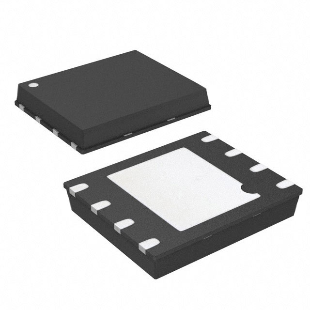
Industry Standard Green (Pb/Halide-free/RoHS Compliant) Package Options
- 8-lead SOIC (0.150” Narrow and 0.208” Wide)
- 8-pad Ultra-Thin DFN (5 x 6 x 0.6 mm)
- 8-ball WLCSP (3 x 2 x 3 grid array)
- Die Wafer Form
- Other Package Options (contact Adesto)
DS-AT25SF161B–188C–01-2021
�Table of Contents
1. Product Overview . . . . . . . . . . . . . . . . . . . . . . . . . . . . . . . . . . . . . . . . . . . . . . . . . . . . . . . . . . . . . . . . . . . . 4
2. Pin Descriptions and Package Pinouts . . . . . . . . . . . . . . . . . . . . . . . . . . . . . . . . . . . . . . . . . . . . . . . . . . . 5
3. Block Diagram . . . . . . . . . . . . . . . . . . . . . . . . . . . . . . . . . . . . . . . . . . . . . . . . . . . . . . . . . . . . . . . . . . . . . . 7
4. Memory Array . . . . . . . . . . . . . . . . . . . . . . . . . . . . . . . . . . . . . . . . . . . . . . . . . . . . . . . . . . . . . . . . . . . . . . . 8
5. Device Operation . . . . . . . . . . . . . . . . . . . . . . . . . . . . . . . . . . . . . . . . . . . . . . . . . . . . . . . . . . . . . . . . . . . 10
5.1 Dual Output Read (1-1-2) . . . . . . . . . . . . . . . . . . . . . . . . . . . . . . . . . . . . . . . . . . . . . . . . . . . . . . . . . 10
5.2 Dual I/O Read (1-2-2) . . . . . . . . . . . . . . . . . . . . . . . . . . . . . . . . . . . . . . . . . . . . . . . . . . . . . . . . . . . . 10
5.3 Quad Output Read (1-1-4) . . . . . . . . . . . . . . . . . . . . . . . . . . . . . . . . . . . . . . . . . . . . . . . . . . . . . . . . 10
5.4 Quad I/O Read (1-4-4) . . . . . . . . . . . . . . . . . . . . . . . . . . . . . . . . . . . . . . . . . . . . . . . . . . . . . . . . . . . 10
6. Commands and Addressing . . . . . . . . . . . . . . . . . . . . . . . . . . . . . . . . . . . . . . . . . . . . . . . . . . . . . . . . . . . 11
7. Read Commands . . . . . . . . . . . . . . . . . . . . . . . . . . . . . . . . . . . . . . . . . . . . . . . . . . . . . . . . . . . . . . . . . . . 13
7.1 Read Array (0Bh and 03h) . . . . . . . . . . . . . . . . . . . . . . . . . . . . . . . . . . . . . . . . . . . . . . . . . . . . . . . . 13
7.2 Dual-Output Read Array (3Bh) . . . . . . . . . . . . . . . . . . . . . . . . . . . . . . . . . . . . . . . . . . . . . . . . . . . . . 14
7.3 Dual-I/O Read Array (BBh) . . . . . . . . . . . . . . . . . . . . . . . . . . . . . . . . . . . . . . . . . . . . . . . . . . . . . . . . 14
7.3.1 Dual-I/O Read Array (BBh) with Continuous Read Mode . . . . . . . . . . . . . . . . . . . . . . . . . . . . 15
7.4 Quad Output Fast Read Array (6Bh). . . . . . . . . . . . . . . . . . . . . . . . . . . . . . . . . . . . . . . . . . . . . . . . . 16
7.5 Quad-I/O Read Array (EBh) . . . . . . . . . . . . . . . . . . . . . . . . . . . . . . . . . . . . . . . . . . . . . . . . . . . . . . . 16
7.5.1 Quad-I/O Read Array (EBh) with Continuous Read Mode . . . . . . . . . . . . . . . . . . . . . . . . . . . 17
7.5.2 Set Burst with Wrap (77h) . . . . . . . . . . . . . . . . . . . . . . . . . . . . . . . . . . . . . . . . . . . . . . . . . . . 18
7.6 Quad-I/O Word Fast Read (E7h). . . . . . . . . . . . . . . . . . . . . . . . . . . . . . . . . . . . . . . . . . . . . . . . . . . . 18
7.6.1 Quad I/O Word Fast Read with “Continuous Read Mode” . . . . . . . . . . . . . . . . . . . . . . . . . . . 19
7.6.2 Quad I/O Word Fast Read with 8-, 16-, 32-, 64-Byte Wrap Around in Standard SPI Mode . . 19
7.7 Read Serial Flash Discoverable Parameter (5Ah) . . . . . . . . . . . . . . . . . . . . . . . . . . . . . . . . . . . . . . 20
8. Program and Erase Commands . . . . . . . . . . . . . . . . . . . . . . . . . . . . . . . . . . . . . . . . . . . . . . . . . . . . . . . . 21
8.1 Byte/Page Program (02h) . . . . . . . . . . . . . . . . . . . . . . . . . . . . . . . . . . . . . . . . . . . . . . . . . . . . . . . . . 21
8.2 Quad Page Program (32h) . . . . . . . . . . . . . . . . . . . . . . . . . . . . . . . . . . . . . . . . . . . . . . . . . . . . . . . . 22
8.3 Block Erase (20h, 52h, or D8h) . . . . . . . . . . . . . . . . . . . . . . . . . . . . . . . . . . . . . . . . . . . . . . . . . . . . . 23
8.4 Chip Erase (60h or C7h) . . . . . . . . . . . . . . . . . . . . . . . . . . . . . . . . . . . . . . . . . . . . . . . . . . . . . . . . . . 23
8.5 Program/Erase Suspend (75h) . . . . . . . . . . . . . . . . . . . . . . . . . . . . . . . . . . . . . . . . . . . . . . . . . . . . . 24
8.6 Program/Erase Resume (7Ah) . . . . . . . . . . . . . . . . . . . . . . . . . . . . . . . . . . . . . . . . . . . . . . . . . . . . . 25
9. Protection Commands and Features . . . . . . . . . . . . . . . . . . . . . . . . . . . . . . . . . . . . . . . . . . . . . . . . . . . . 26
9.1 Write Enable (06h) . . . . . . . . . . . . . . . . . . . . . . . . . . . . . . . . . . . . . . . . . . . . . . . . . . . . . . . . . . . . . . 26
9.2 Write Disable (04h) . . . . . . . . . . . . . . . . . . . . . . . . . . . . . . . . . . . . . . . . . . . . . . . . . . . . . . . . . . . . . . 26
9.3 Non-Volatile Protection . . . . . . . . . . . . . . . . . . . . . . . . . . . . . . . . . . . . . . . . . . . . . . . . . . . . . . . . . . . 27
9.4 Protected States and the Write Protect Pin. . . . . . . . . . . . . . . . . . . . . . . . . . . . . . . . . . . . . . . . . . . . 28
9.5 Enable Reset (66h) and Reset Device (99h). . . . . . . . . . . . . . . . . . . . . . . . . . . . . . . . . . . . . . . . . . . 29
10. Security Register Commands . . . . . . . . . . . . . . . . . . . . . . . . . . . . . . . . . . . . . . . . . . . . . . . . . . . . . . . . . 30
10.1 Read Unique ID Number (4Bh) . . . . . . . . . . . . . . . . . . . . . . . . . . . . . . . . . . . . . . . . . . . . . . . . . . . . . 30
10.2 Erase Security Registers (44h) . . . . . . . . . . . . . . . . . . . . . . . . . . . . . . . . . . . . . . . . . . . . . . . . . . . . . 30
10.3 Program Security Registers (42h) . . . . . . . . . . . . . . . . . . . . . . . . . . . . . . . . . . . . . . . . . . . . . . . . . . . 31
10.4 Read Security Registers (48h) . . . . . . . . . . . . . . . . . . . . . . . . . . . . . . . . . . . . . . . . . . . . . . . . . . . . . 32
AT25SF161B
DS-AT25SF161B–188C–01-2021
2
�Table of Contents
11. Status Register Commands . . . . . . . . . . . . . . . . . . . . . . . . . . . . . . . . . . . . . . . . . . . . . . . . . . . . . . . . . . .
11.1 Read Status Register (05h, 35h, and 15h) . . . . . . . . . . . . . . . . . . . . . . . . . . . . . . . . . . . . . . . . . . . .
11.1.1 SRP1, SRP0 Bits . . . . . . . . . . . . . . . . . . . . . . . . . . . . . . . . . . . . . . . . . . . . . . . . . . . . . . . . . .
11.1.2 CMP, BP4, BP3, BP2, BP1, BP0 Bits . . . . . . . . . . . . . . . . . . . . . . . . . . . . . . . . . . . . . . . . . . .
11.1.3 WEL Bit . . . . . . . . . . . . . . . . . . . . . . . . . . . . . . . . . . . . . . . . . . . . . . . . . . . . . . . . . . . . . . . . . .
11.1.4 RDY/BSY Bit . . . . . . . . . . . . . . . . . . . . . . . . . . . . . . . . . . . . . . . . . . . . . . . . . . . . . . . . . . . . . .
11.1.5 LB3, LB2, LB1 Bits . . . . . . . . . . . . . . . . . . . . . . . . . . . . . . . . . . . . . . . . . . . . . . . . . . . . . . . . .
11.1.6 E_SUS Bit . . . . . . . . . . . . . . . . . . . . . . . . . . . . . . . . . . . . . . . . . . . . . . . . . . . . . . . . . . . . . . . .
11.1.7 P_SUS Bit . . . . . . . . . . . . . . . . . . . . . . . . . . . . . . . . . . . . . . . . . . . . . . . . . . . . . . . . . . . . . . . .
11.1.8 QE Bit . . . . . . . . . . . . . . . . . . . . . . . . . . . . . . . . . . . . . . . . . . . . . . . . . . . . . . . . . . . . . . . . . . .
33
33
35
36
36
36
36
36
37
37
11.2 Write Status Register (01h, 31h, 11h) . . . . . . . . . . . . . . . . . . . . . . . . . . . . . . . . . . . . . . . . . . . . . . . . 37
11.3 Write Enable for Volatile Status Register (50h). . . . . . . . . . . . . . . . . . . . . . . . . . . . . . . . . . . . . . . . . 38
12. Other Commands and Functions . . . . . . . . . . . . . . . . . . . . . . . . . . . . . . . . . . . . . . . . . . . . . . . . . . . . . . . 39
12.1 Read Manufacturer and Device ID (9Fh) . . . . . . . . . . . . . . . . . . . . . . . . . . . . . . . . . . . . . . . . . . . . . 39
12.2 Read ID (Legacy Command) (90h) . . . . . . . . . . . . . . . . . . . . . . . . . . . . . . . . . . . . . . . . . . . . . . . . . . 40
12.3 Dual I/O Read Manufacture ID/ Device ID (92h) . . . . . . . . . . . . . . . . . . . . . . . . . . . . . . . . . . . . . . . . 41
12.4 Quad I/O Read Manufacture ID / Device ID (94h). . . . . . . . . . . . . . . . . . . . . . . . . . . . . . . . . . . . . . . 42
12.5 Deep Power-Down (B9h) . . . . . . . . . . . . . . . . . . . . . . . . . . . . . . . . . . . . . . . . . . . . . . . . . . . . . . . . . 43
12.6 Resume from Deep Power-Down (ABh) . . . . . . . . . . . . . . . . . . . . . . . . . . . . . . . . . . . . . . . . . . . . . . 44
12.6.1 Resume from Deep Power-Down and Read Device ID (ABh) . . . . . . . . . . . . . . . . . . . . . . . . 44
12.7 Hold Function . . . . . . . . . . . . . . . . . . . . . . . . . . . . . . . . . . . . . . . . . . . . . . . . . . . . . . . . . . . . . . . . . . 45
13. Electrical Specifications . . . . . . . . . . . . . . . . . . . . . . . . . . . . . . . . . . . . . . . . . . . . . . . . . . . . . . . . . . . . . . 46
13.1 Absolute Maximum Ratings* . . . . . . . . . . . . . . . . . . . . . . . . . . . . . . . . . . . . . . . . . . . . . . . . . . . . . . . 46
13.2 DC and AC Operating Range . . . . . . . . . . . . . . . . . . . . . . . . . . . . . . . . . . . . . . . . . . . . . . . . . . . . . . 46
13.3 DC Characteristics . . . . . . . . . . . . . . . . . . . . . . . . . . . . . . . . . . . . . . . . . . . . . . . . . . . . . . . . . . . . . . 46
13.4 AC Characteristics - Maximum Clock Frequencies . . . . . . . . . . . . . . . . . . . . . . . . . . . . . . . . . . . . . . 47
13.5 AC Characteristics - All Other Parameters . . . . . . . . . . . . . . . . . . . . . . . . . . . . . . . . . . . . . . . . . . . . 47
13.6 Program and Erase Characteristics . . . . . . . . . . . . . . . . . . . . . . . . . . . . . . . . . . . . . . . . . . . . . . . . . 48
13.7 Power Up Conditions. . . . . . . . . . . . . . . . . . . . . . . . . . . . . . . . . . . . . . . . . . . . . . . . . . . . . . . . . . . . . 48
13.8 Input Test Waveforms and Measurement Levels . . . . . . . . . . . . . . . . . . . . . . . . . . . . . . . . . . . . . . . 49
13.9 Output Test Load. . . . . . . . . . . . . . . . . . . . . . . . . . . . . . . . . . . . . . . . . . . . . . . . . . . . . . . . . . . . . . . . 49
14. AC Waveforms . . . . . . . . . . . . . . . . . . . . . . . . . . . . . . . . . . . . . . . . . . . . . . . . . . . . . . . . . . . . . . . . . . . . . 50
15. Ordering Information . . . . . . . . . . . . . . . . . . . . . . . . . . . . . . . . . . . . . . . . . . . . . . . . . . . . . . . . . . . . . . . . 52
16. Packaging Information . . . . . . . . . . . . . . . . . . . . . . . . . . . . . . . . . . . . . . . . . . . . . . . . . . . . . . . . . . . . . . . 53
16.1 8S1 – 0.150” Narrow JEDEC SOIC. . . . . . . . . . . . . . . . . . . . . . . . . . . . . . . . . . . . . . . . . . . . . . . . . . 53
16.2 8S2 – 8-lead, 0.208” Wide EIAJ SOIC . . . . . . . . . . . . . . . . . . . . . . . . . . . . . . . . . . . . . . . . . . . . . . . 54
16.3 8MA1 – UDFN . . . . . . . . . . . . . . . . . . . . . . . . . . . . . . . . . . . . . . . . . . . . . . . . . . . . . . . . . . . . . . . . . . 55
16.4 8-WLCSP — 8-ball 3 x 2 x 3 WLCSP . . . . . . . . . . . . . . . . . . . . . . . . . . . . . . . . . . . . . . . . . . . . . . . . 56
17. Revision History . . . . . . . . . . . . . . . . . . . . . . . . . . . . . . . . . . . . . . . . . . . . . . . . . . . . . . . . . . . . . . . . . . . . 57
AT25SF161B
DS-AT25SF161B–188C–01-2021
3
�1.
Product Overview
The Adesto® AT25SF161B is a serial interface Flash memory device designed for a wide variety of high-volume
consumer-based applications in which program code is shadowed from Flash memory into embedded or external
RAM for execution. The flexible erase architecture of the AT25SF161B also is ideal for data storage, eliminating
the need for additional data storage devices.
The AT25SF161B erase block sizes are optimized to meet the needs of today's code and data storage
applications. This means memory space can be used much more efficiently. Because certain code modules and
data storage segments must reside in their own erase regions, the wasted and unused memory space that occurs
with large-block-erase Flash memory devices can be reduced greatly. This increased memory space allows
additional code routines and data storage segments to be added, while maintaining the same overall device
density.
This device also contains three Security Register pages for unique device serialization, system-level Electronic
Serial Number (ESN) storage, locked key storage, etc. These pages can be locked individually.
AT25SF161B
DS-AT25SF161B–188C–01-2021
4
�2.
Pin Descriptions and Package Pinouts
Table 2-1.
Pin Descriptions
Symbol
Name and Function
Asserted
State
Type
Low
Input
-
Input
-
Input/Output
-
Input/Output
-
Input/Output
CHIP SELECT: Asserting the CS pin selects the device. When the CS pin is
deasserted, the device is deselected and normally be placed in standby mode.
CS
SCK
A high-to-low transition on the CS pin is required to start an operation; a low-tohigh transition is required to end an operation. When ending an internally selftimed operation, such as a program or erase cycle, the device does not enter the
standby mode until the operation is complete.
SERIAL CLOCK: This pin provides a clock to the device. Command, address, and
input data present on the SI pin is latched in on the rising edge of SCK, while
output data on the SO pin is clocked out on the falling edge of SCK.
SERIAL INPUT: The SI pin is used for all data input, including command and
address sequences. Data on the SI pin is always latched in on the rising edge of
SCK.
SI (I/O0)
With the Dual-Output and Quad-Output Read commands, the SI pin becomes an
output pin (I/O0) in conjunction with other pins to allow two or four bits of data (on
I/O3-0) to be clocked in on every falling edge of SCK.
Data present on the SI pin is ignored whenever the device is deselected (CS is
deasserted).
SERIAL OUTPUT: Data on the SO pin is clocked out on the falling edge of SCK.
SO (I/O1)
With the Dual-Output Read commands, the SO pin remains an output pin (I/O0) in
conjunction with other pins to allow two bits of data (on I/O1-0) to be clocked in on
every falling edge of SCK.
The SO pin is in a high-impedance state whenever the device is deselected (CS is
deasserted).
WRITE PROTECT: The WP pin controls the hardware locking feature of the
device.
WP
(I/O2)
With the Quad-Input Byte/Page Program command, the WP pin becomes an input
pin (I/O2) and, along with other pins, allows four bits (on I/O3-0) of data to be
clocked in on every rising edge of SCK. With the Quad-Output Read commands,
the WP Pin becomes an output pin (I/O2) in conjunction with other pins to allow
four bits of data (on I/O33-0) to be clocked in on every falling edge of SCK.
The WP pin is internally pulled-high and can be left floating if hardware-controlled
protection is not used; however, it is recommended that the WP pin also be
externally connected to VCC whenever possible.
AT25SF161B
DS-AT25SF161B–188C–01-2021
5
�Table 2-1.
Pin Descriptions (continued)
Symbol
Name and Function
Asserted
State
Type
-
Input/Output
HOLD: The HOLD pin temporarily pauses serial communication without
deselecting or resetting the device. While the HOLD pin is asserted, transitions on
the SCK pin and data on the SI pin are ignored, and the SO pin is in a highimpedance state.
HOLD
(I/O3)
The CS pin must be asserted, and the SCK pin must be in the low state, for a Hold
condition to start. A Hold condition pauses serial communication only and does not
have an affect on internally self-timed operations, such as a program or erase
cycle. See “Hold Function”, on page 45 for additional details on the Hold
operation.
With the Quad-Input Byte/Page Program command, the HOLD pin becomes an
input pin (I/O3) and, along with other pins, allows four bits (on I/O3-0) of data to be
clocked in on every rising edge of SCK. With the Quad-Output Read commands,
the HOLD pin becomes an output pin (I/O3) in conjunction with other pins to allow
four bits of data (on I/O33-0) to be clocked in on every falling edge of SCK.
The HOLD pin is internally pulled-high and can be left floating if the Hold function is
not used. It is recommended, however, that the HOLD pin is externally connected
to VCC whenever possible.
VCC
DEVICE POWER SUPPLY: The VCC pin supplies the source voltage to the device.
-
Power
GND
GROUND: The ground reference for the power supply. Connect GND to the
system ground.
-
Power
Figure 2-1. 8-SOIC (0.150” and 0.208”) — Top View
CS
SO (IO1)
WP (IO2)
GND
1
2
3
4
VCC
HOLD (IO3)
SCK
SI (IO0)
8
7
6
5
Figure 2-3. 8-UDFN — Top View
CS
SO (IO1)
WP (IO2)
GND
1
2
3
4
8
7
6
5
VCC
HOLD (IO3)
SCK
SI (IO0)
Figure 2-2. 8-ball WLCSP (3 x 2 x 3) — Bottom View
CS
VCC
A3
GND
A1
SO
B2
HOLD
C3
SI
C1
WP
D2
SCK
E3
E1
AT25SF161B
DS-AT25SF161B–188C–01-2021
6
�3.
Block Diagram
Figure 3-1. Block Diagram
Control and
Protection Logic
CS
I/O Buffers
and Latches
SRAM
Data Buffer
SI (I/O0)
SO (I/O1)
WP (I/O2)
Interface
Control
And
Logic
Address Latch
SCK
Y-Decoder
Y-Gating
X-Decoder
Flash
Memory
Array
HOLD
(I/O3)
Note: I/O3-0 pin naming convention is used for Dual-I/O and Quad-I/O commands.
AT25SF161B
DS-AT25SF161B–188C–01-2021
7
�4.
Memory Array
To provide the greatest flexibility, the memory array of the AT25SF161B can be erased in four levels of granularity,
including a full-chip erase. The size of the erase blocks is optimized for both code and data storage applications,
allowing both code and data segments to reside in their own erase regions. Note that in the following figures, the
(Bxxx) value in parentheses indicates the block number.
Table 4-1.
Device Memory Map — Block Erase Address Ranges
64 kbyte Block Erase (D8h)
32 kbyte Block Erase (52h)
4 kbyte Block Erase (20h)
Block Address Range
4 kbytes (B511)
1FF000h - 1FFFFFh
4 kbytes (B510)
1FE000h - 1FEFFFh
4 kbytes (B509)
1FD000h - 1FDFFFh
32 kbytes
4 kbytes (B508)
1FC000h - 1FCFFFh
(block 63)
4 kbytes (B507)
1FB000h - 1FBFFFh
4 kbytes (B506)
1FA000h - 1FAFFFh
4 kbytes (B505)
1F9000h - 1F9FFFh
64 kbytes
4 kbytes (B504)
1F8000h - 1F8FFFh
(block 31)
4 kbytes (B503)
1F7000h - 1F7FFFh
4 kbytes (B502)
1F6000h - 1F6FFFh
4 kbytes (B501)
1F5000h - 1F5FFFh
32 kbytes
4 kbytes (B500)
1F4000h - 1F4FFFh
(block 62)
4 kbytes (B499)
1F3000h - 1F3FFFh
4 kbytes (B498)
1F2000h - 1F2FFFh
4 kbytes (B497)
1F1000h - 1F1FFFh
4 kbytes (B496)
1F0000h - 1F0FFFh
64 kbytes (block 30)
32 kbytes (block 61)
4 kbytes (B495)
1EF000h - 1EFFFFh
to
to
to
to
64 kbytes (block 1)
32 kbytes (block 2)
4 kbytes (B16)
010000h - 010FFFh
4 kbytes (B15)
00F000h - 00FFFFh
4 kbytes (B14)
00E000h - 00EFFFh
4 kbytes (B13)
00D000h - 00DFFFh
32 kbytes
4 kbytes (B12)
00C000h - 00CFFFh
(block 1)
4 kbytes (B11)
00B000h - 00BFFFh
4 kbytes (B10)
00A000h - 00AFFFh
4 kbytes (B9)
009000h - 009FFFh
64 kbytes
4 kbytes (B8)
008000h - 008FFFh
(block 0
4 kbytes (B7)
007000h - 007FFFh
4 kbytes (B6)
006000h - 006FFFh
4 kbytes (B5)
005000h - 005FFFh
32 kbytes
4 kbytes (B4)
004000h - 004FFFh
(block 0)
4 kbytes (B3)
003000h - 003FFFh
4 kbytes (B2)
002000h - 002FFFh
4 kbytes (B1)
001000h - 001FFFh
4 kbytes (B0)
000000h - 000FFFh
AT25SF161B
DS-AT25SF161B–188C–01-2021
8
�Table 4-2.
Device Memory Map — Page Program Address Ranges
4 kbytes Blocks
256 Byte Page
1 - 256 Byte Page Program
4 kbytes (B511)
256 Bytes
1FFF00h - 1FFFFFh
4 kbytes (B510)
256 Bytes
1FFE00h - 1FFEFFh
4 kbytes (B509)
256 Bytes
1FFD00h - 1FFDFFh
4 kbytes (B508)
256 Bytes
1FFC00h - 1FFCFFh
4 kbytes (B507)
256 Bytes
1FFB00h - 1FFBFFh
4 kbytes (B506)
256 Bytes
1FFA00h - 1FFAFFh
4 kbytes (B505)
256 Bytes
1FF900h - 1FF9FFh
4 kbytes (B504)
256 Bytes
1FF800h - 1FF8FFh
4 kbytes (B503)
256 Bytes
1FF700h - 1FF7FFh
4 kbytes (B502)
256 Bytes
1FF600h - 1F6FFFh
4 kbytes (B501)
256 Bytes
1FF500h - 1FF5FFh
4 kbytes (B500)
256 Bytes
1FF400h - 1FF4FFh
4 kbytes (B499)
256 Bytes
1FF300h - 1FF3FFh
4 kbytes (B498)
256 Bytes
1FF200h - 1FF2FFh
4 kbytes (B497)
256 Bytes
1FF100h - 1FF1FFh
4 kbytes (B496)
256 Bytes
1FF000h - 1FF0FFh
4 kbytes (B494)
.
.
.
to
.
.
.
4 kbytes (B16)
.
.
.
4 kbytes (B15)
256 Bytes
000F00h - 000FFFh
4 kbytes (B14)
256 Bytes
000E00h - 000EFFh
4 kbytes (B13)
256 Bytes
000D00h - 000DFFh
4 kbytes (B12)
256 Bytes
000C00h - 000CFFh
4 kbytes (B11)
256 Bytes
000B00h - 000BFFh
4 kbytes (B10)
256 Bytes
000A00h - 000AFFh
4 kbytes (B9)
256 Bytes
000900h - 0009FFh
4 kbytes (B8)
256 Bytes
000800h - 0008FFh
4 kbytes (B7)
256 Bytes
000700h - 0007FFh
4 kbytes (B6)
256 Bytes
000600h - 0006FFh
4 kbytes (B5)
256 Bytes
000500h - 0005FFh
4 kbytes (B4)
256 Bytes
000400h - 0004FFh
4 kbytes (B3)
256 Bytes
000300h - 0003FFh
4 kbytes (B2)
256 Bytes
000200h - 0002FFh
4 kbytes (B1)
256 Bytes
000100h - 0001FFh
4 kbytes (B0)
256 Bytes
000000h - 0000FFh
AT25SF161B
DS-AT25SF161B–188C–01-2021
9
�5.
Device Operation
The AT25SF161B is controlled by a set of instructions sent from a host controller, SPI Master. The SPI Master
communicates with the AT25SF161B through the SPI bus, which consists of four pins: Chip Select (CS), Serial
Clock (SCK), Serial Input (SI), and Serial Output (SO).
The SPI protocol defines a total of four modes of operation (mode 0, 1, 2, or 3). The AT25SF161B supports the two
most common modes, SPI modes 0 and 3. For these modes, data is latched in on the rising edge of SCK and
output on the falling edge of SCK.
Figure 5-1. SPI Mode 0 and 3
CS
SCK
SI
MSB
SO
5.1
LSB
MSB
LSB
Dual Output Read (1-1-2)
The AT25SF161B supports Dual Output (1-1-2) transfers, which enhance overall throughput over the standard SPI
mode. This mode transfers the command and address on the SI pin, but the data are transferred on the SI and SO
pins. This means that only half the number of clocks are required to transfer the data.
5.2
Dual I/O Read (1-2-2)
The AT25SF161B supports Dual I/O (1-2-2) transfers, which enhance throughput over the standard SPI mode.
This mode transfers the command on the SI pin, but the address and data are transferred on the SI and SO pins.
This means that only half the number of clocks are required to transfer the address and data.
5.3
Quad Output Read (1-1-4)
The AT25SF161B supports Quad Output (1-1-4) transfers, which enhance overall throughput over the standard
SPI mode. This mode transfers the command and address on the SI pin, but the data is transferred on the SI, SO,
WP, and HOLD pins. This means that only a quarter the number of clocks are required to transfer the data. With
the Quad-Output Read Array command, the SI, WP, and HOLD pins become outputs along with the SO pin.
5.4
Quad I/O Read (1-4-4)
The AT25SF161B supports Quad I/O (1-4-4) transfers, which enhance throughput over the standard SPI mode.
This mode transfers the command on the SI pin, but the address and data are transferred on the SI, SO, WP, and
HOLD pins. This means that only a quarter of the number of clocks are required to transfer the address and data.
With the Quad I/O Read Array command, the SI, WP, and HOLD and SO pins become inputs during the address
transfer, and switch to outputs during the data transfer.
AT25SF161B
DS-AT25SF161B–188C–01-2021
10
�6.
Commands and Addressing
A valid instruction or operation must be started by first asserting the CS pin. After the CS pin has been asserted,
the host controller must clock out a valid eight-bit opcode on the SPI bus. Following the opcode, instructiondependent information, such as address and data bytes, can be clocked out by the host controller. All opcode,
address, and data bytes are transferred with the most-significant bit (MSB) first. An operation is ended by
deasserting the CS pin.
Opcodes not supported by the AT25SF161B are ignored by the device, and no operation is started. The device
continues to ignore any data presented on the SI pin until the start of the next operation (CS pin being deasserted
and then reasserted). If the CS pin is deasserted before complete opcode, and address information is sent to the
device, no operation is performed, and the device returns to the idle state and waits for the next operation.
Addressing of the device requires three bytes of information to be sent, representing address bits A23-A0. Since
the upper address limit of the AT25SF161B memory array is 1FFFFFh, address bits A23-A21 are ignored by the
device.
Table 6-1.
AT25SF161B Command Table
Command
Opcode
Bus Transfer
Type
(OP-AD-DA) 1
Enable Reset
66h
1-0-0
N
Reset Device
99h
1-0-0
Deep Power-down
B9h
Release Power-down
Wait Cycle
Dummy Clocks
Number of
Data Bytes
0
0
0
N
0
0
0
1-0-0
N
0
0
0
ABh
1-0-0
N
0
0
0
Normal Read Data
03h
1-1-1
N
0
0
1+
Fast Read
0Bh
1-1-1
N
0
8
1+
Dual Output Fast read
3Bh
1-1-2
N
0
8
1+
Dual I/O Fast read
BBh
1-2-2
Y
4
0
1+
Dual I/O Fast read (Continuous Mode)
BBh
0-2-2
Y
4
0
1+
Quad Output Fast read
6Bh
1-1-4
N
0
8
1+
Quad I/O Fast read
EBh
1-4-4
Y
2
4
1+
Quad I/O Fast read (Continuous Mode)
EBh
0-4-4
Y
2
4
1+
Word Read Quad I/O
E7h
1-4-4
Y
2
2
1+
Word Read Quad I/O (Continuous
Mode)
E7h
0-4-4
Y
2
2
1+
Set Burst With Wrap
77h
1-0-4
N
0
6
1, D[6:4]
Write Enable
06h
1-0-0
N
0
0
0
Volatile SR Write Enable
50h
1-0-0
N
0
0
0
Write Disable
04h
1-0-0
N
0
0
0
Command Name
Mode Bit Mode Bit
Present
Clocks
System Commands
Read Commands
Write Commands
AT25SF161B
DS-AT25SF161B–188C–01-2021
11
�Table 6-1.
AT25SF161B Command Table (continued)
Command
Opcode
Bus Transfer
Type
(OP-AD-DA) 1
Page Program
02h
1-1-1
N
Quad Page Program
32h
1-1-4
Block Erase (4KB)
20h
Block Erase (32KB)
Block Erase (64KB)
Wait Cycle
Dummy Clocks
Number of
Data Bytes
0
0
1+
N
0
0
1+
1-1-0
N
0
0
0
52h
1-1-0
N
0
0
0
D8h
1-1-0
N
0
0
0
C7h/60h
1-0-0
N
0
0
0
Program/Erase Suspend
75h
1-0-0
N
0
0
0
Program/Erase Resume
7Ah
1-0-0
N
0
0
0
Read Status Register 1
05h
1-0-1
N
0
0
1
Read Status Register 2
35h
1-0-1
N
0
0
1
Read Status Register 3
15h
1-0-1
N
0
0
1
Write Status Register 1
01h
1-0-1
N
0
0
1
Write Status Register 2
31h
1-0-1
N
0
0
1
Write Status Register 3
11h
1-0-1
N
0
0
1
Manufacturer/Device ID
90h
1-1-1
N
0
0
2
Mfgr./Device ID Dual I/O
92h
1-2-2
N
0
4
2
Mfgr./Device ID Quad I/O
94h
1-4-4
N
0
4
2
Read JEDEC ID
9Fh
1-0-1
N
0
0
3
Read Serial Flash Discoverable
Parameter
5Ah
1-1-1
N
0
8
1+
Erase Security Registers
44h
1-1-0
N
0
0
0
Program Security Registers
42h
1-1-1
N
0
0
1+
Read Security Registers
48h
1-1-1
N
0
8
1+
Read Unique ID Number
4Bh
1-0-1
N
0
32
1+
Command Name
Mode Bit Mode Bit
Present
Clocks
Program Commands
Erase Commands
Chip Erase
Suspend/Resume Commands
Status Register Commands
Device Information Commands
OTP Commands
1. OP = Opcode (command number), AD = Address. DA = Data. 0 indicates the corresponding transfer does not occur in that command. 1 indicates the transfer
does occur. For example, 1-0-0 indicates a command transfer occurs, but no address or data transfers occur.
Op: Opcode or Commands (8-bits): 0 → No Opcode [continuous Read], 1 → 8 clocks for Opcode, 2 → 4 clocks for Opcode, 4 → 2 clocks for opcode.
AD: Address (24-bits) Only: 0 → No address, Opcode only operation, 1 → 24 clocks for Address, 2 → 12 clocks for address, 4 → 6 clocks for address.
AD: Address (24-bits) + Mode (8-bits): 2 → 12 clocks for address, 4 clocks for mode [BBh only], 4 → 6 clocks for address, 2 clocks for mode [EBh and E7h].
DA: Data(8-bits): 1 → 8 clocks for Byte, 2 → 4 clocks for Byte, 4 → 2 clocks for Byte.
AT25SF161B
DS-AT25SF161B–188C–01-2021
12
�7.
Read Commands
7.1
Read Array (0Bh and 03h)
The Read Array command can be used to sequentially read a continuous stream of data from the device by
providing the clock pin once the initial starting address is specified. The device incorporates an internal address
counter that automatically increments every clock cycle.
To perform the Read Array operation, the CS pin first must be asserted, and the appropriate opcode (0Bh or 03h)
must be clocked into the device. After the opcode has been clocked in, the three address bytes must be clocked in
to specify the starting address location of the first byte to read within the memory array. If the 0Bh opcode is used
for the Read Array operation, an additional dummy byte must be clocked into the device after the three address
bytes.
After the three address bytes (and the dummy byte, if using opcode 0Bh) have been clocked in, additional clock
cycles result in data being output on the SO pin. The data is always output with the MSB of a byte first. When the
last byte (1FFFFFh) of the memory array has been read, the device continues reading back at the beginning of the
array (000000h). No delays are incurred when wrapping around from the end of the array to the beginning of the
array.
Deasserting the CS pin terminates the read operation and puts the SO pin into high-impedance state. The CS pin
can be deasserted at any time and does not require a full byte of data be read.
Figure 7-1. Read Array - 03h Opcode
CS
0
1
2
3
4
5
6
7
8
9
10 11 12
29 30 31 32 33 34 35 36 37 38 39 40
SCK
OPCODE
SI
0
0
0
0
0
ADDRESS BITS A23-A0
0
1
A
1
MSB
A
A
A
A
A
A
A
A
MSB
DATA BYTE 1
HIGH-IMPEDANCE
SO
D
D
D
D
D
D
D
MSB
D
D
D
MSB
Figure 7-2. Read Array - 0Bh Opcode
CS
0
1
2
3
4
5
6
7
8
9
10 11 12
29 30 31 32 33 34 35 36 37 38 39 40 41 42 43 44 45 46 47 48
SCK
OPCODE
SI
0
0
0
0
1
ADDRESS BITS A23-A0
0
MSB
1
1
A
MSB
A
A
A
A
A
A
DON'T CARE
A
A
X
X
X
X
X
X
X
X
MSB
DATA BYTE 1
SO
HIGH-IMPEDANCE
D
MSB
D
D
D
D
D
D
D
D
D
MSB
AT25SF161B
DS-AT25SF161B–188C–01-2021
13
�7.2
Dual-Output Read Array (3Bh)
The Dual-Output Read Array command is similar to the standard Read Array command; it can be used to
sequentially read a continuous stream of data from the device by providing the clock pin once the initial starting
address has been specified. Unlike the standard Read Array command, the Dual-Output Read Array command
allows two bits of data to be clocked out of the device on every clock cycle, rather than just one.
To perform the Dual-Output Read Array operation, the CS pin must first be asserted; then, the opcode 3Bh must
be clocked into the device. After the opcode has been clocked in, the three address bytes must be clocked in to
specify the location of the first byte to read within the memory array. Following the three address bytes, a single
dummy byte also must be clocked into the device.
After the three address bytes and the dummy byte have been clocked in, additional clock cycles output data on
both the SO and SI pins. The data is output with the MSB of a byte first, and the MSB is output on the SO pin.
During the first clock cycle, bit seven of the first data byte is output on the SO pin, while bit six of the same data
byte is output on the SI pin. During the next clock cycle, bits five and four of the first data byte are output on the SO
and SI pins, respectively. The sequence continues with each byte of data being output after every four clock
cycles. When the last byte (1FFFFFh) of the memory array has been read, the device continues reading from the
beginning of the array (000000h). There are no delays because of wrapping around from the end of the array to the
beginning of the array. Deasserting the CS pin terminates the read operation and puts the SO and SI pins into a
high-impedance state. The CS pin can be deasserted at any time and does not require that a full byte of data be
read.
Figure 7-3. Dual-Output Read Array
CS
0
1
2
3
4
5
6
7
8
9
10 11 12
29 30 31 32 33 34 35 36 37 38 39 40 41 42 43 44 45 46 47 48
SCK
23&2'(
SI (SIO)
0
0
1
1
1
0
$''5(66�%,76�$���$��
1
06%
SO
+,*+�,03('$1&(
1
A
06%
A
A
A
A
A
A
287387
'$7$�%


 工商网监
湘ICP备2023018690号
工商网监
湘ICP备2023018690号
