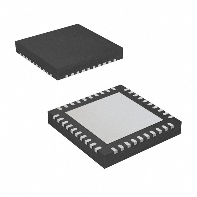
IDTCSPUA877A
1.8V PLL DIFFERENTIAL 1:10 SDRAM CLOCK DRIVER
COMMERCIAL TEMPERATURE RANGE
1.8V PHASE LOCKED LOOP
DIFFERENTIAL 1:10 SDRAM
CLOCK DRIVER
IDTCSPUA877A
DESCRIPTION:
FEATURES:
The CSPUA877A is a PLL based clock driver that acts as a zero delay buffer
to distribute one differential clock input pair(CLK, CLK ) to 10 differential
output pairs (Y [0:9], Y [0:9]) and one differential pair of feedback clock output
(FBOUT, FBOUT). External feedback pins (FBIN, FBIN) for synchronization
of the outputs to the input reference is provided. OE, OS, and AVDD control the
power-down and test mode logic. When AVDD is grounded, the PLL is turned
off and bypassed for test mode purposes. When the differential clock inputs
(CLK, CLK) are both at logic low, this device will enter a low power-down mode.
In this mode, the receivers are disabled, the PLL is turned off, and the output
clock drivers are disabled, resulting in a clock driver current consumption of less
than 500μA.
The CSPUA877A requires no external components and has been optimised
for very low phase error, skew, and jitter, while maintaining frequency and duty
cycle over the operating voltage and temperature range. The CSPUA877 ,
designed for use in both module assemblies and system motherboard based
solutions, provides an optimum high-performance clock source.
The CSPUA877A is available in Commercial Temperature Range (0°C to
+70°C). See Ordering Information for details.
• 1 to 10 differential clock distribution
• Optimized for clock distribution in DDR2 (Double Data Rate)
SDRAM applications
• Operating frequency: 125MHz to 410MHz
• Stabilization time:
很抱歉,暂时无法提供与“CSPUA877ANLG”相匹配的价格&库存,您可以联系我们找货
免费人工找货