DAC1617D1G0
Dual 16-bit DAC, LVDS interface, up to 1 Gsps, x2, x4 and x8
interpolating
Rev. 4 — 12 December 2012
Product data sheet
1. General description
The DAC1617D1G0 is a high-speed 16-bit dual channel Digital-to-Analog Converter
(DAC) with selectable ×2, ×4 and ×8 interpolation filters. The device is optimized for
multi-carrier and broadband wireless transmitters at sample rates of up to 1 Gsps.
Supplied from a 3.3 V and a 1.8 V source, the DAC1617D1G0 integrates a differential
scalable output current up to 34 mA.
The Serial Peripheral Interface (SPI) provides full control of the DAC1617D1G0.
The DAC1617D1G0 integrates a Low Voltage Differential Signaling (LVDS) Double Data
Rate (DDR) receiver interface, with an on-chip 100 Ω termination. The LVDS DDR
interface accepts a multiplex input data stream such as interleaved or folded. An internal
LVDS input auto-calibration ensures the robustness and stability of the interface.
Digital on-chip modulation converts the complex I and Q inputs from baseband to IF. A
40-bit Numerically Controlled Oscillator (NCO) sets the mixer frequency. High resolution
internal gain, phase and offset control provide outstanding image and Local Oscillator
(LO) signal rejection at the system analog modulator output.
An inverse (sin x) / x function ensures a controlled flatness 0.5 dB for high bandwidths at
the DAC output.
Multiple device synchronization allows synchronization of the outputs of multiple DAC
devices. MDS guarantees a maximum skew of one output clock period between several
devices.
The DAC1617D1G0 includes a very low noise capacitor-free integrated Phase-Locked
Loop (PLL) multiplier which generates a DAC clock rate from the LVDS clock rate.
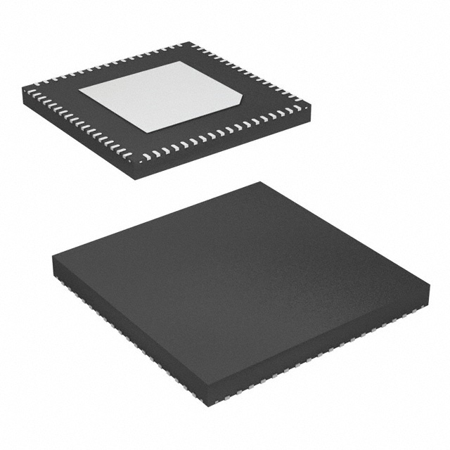
The DAC1617D1G0 is available in an HVQFN72 package (10 mm × 10 mm).
®
�DAC1617D1G0
Integrated Device Technology
Dual 16-bit DAC: up to 1 Gsps; x2, x4 and x8 interpolating
2. Features and benefits
� Dual-channel 16-bit resolution
�
�
�
�
�
�
�
�
�
�
� Synchronization of multiple DAC
devices
1 Gsps maximum update rate
� 3-wire or 4-wire mode SPI interface
Selectable ×2, ×4 and ×8 interpolation
� Differential scalable output current from
filters
8.1 mA to 34 mA
Very low noise capacitor-free integrated � External analog offset control
Phase-Locked Loop (PLL)
(10-bit auxiliary DACs)
Embedded Numerically Controlled
� High resolution internal digital gain and
Oscillator (NCO) with 40-bit
offset control to support high
programmable frequency
performance IQ-modulator image
rejection
Embedded complex(I/Q) digital IF
� Internal phase correction
modulator
1.8 V and 3.3 V power supplies
� Inverse (sin x) / x function
LVDS DDR compatible input interface
� Power-down mode and Sleep mode;
with on-chip 100 Ω terminations
5-bit NCO low-power mode
LVDS DDR input clock up to 370 MHz
� On-chip 1.25 V reference
LVDS or LVPECL compatible DAC clock � Industrial temperature range −40 °C to
+85 °C
Interleaved or folded I and Q data input � 72 pins small form factor HVQFN
mode
package
3. Applications
�
�
�
�
�
�
�
Wireless infrastructure: LTE, WiMAX, GSM, CDMA, WCDMA, TD-SCDMA
Communications: LMDS/MMDS, point-to-point
Direct Digital Synthesis (DDS)
Broadband wireless systems
Digital radio links
Instrumentation
Automated Test Equipment (ATE)
4. Ordering information
Table 1.
Ordering information
Type number
DAC1617D1G0HN
Package
Name
Description
Version
HVQFN72
plastic thermal enhanced very thin quad flat package; no leads;
72 terminals; body 10 × 10 × 0.85 mm
SOT813-3
DAC1617D1G0
Product data sheet
© IDT 2012. All rights reserved.
Rev. 4 — 12 December 2012
2 of 78
�xxxxxxxxxxxxxxxxxxxxx xxxxxxxxxxxxxxxxxxxxxxxxxx xxxxxxx x x x xxxxxxxxxxxxxxxxxxxxxxxxxxxxxx xxxxxxxxxxxxxxxxxxx xx xx xxxxx
xxxxxxxxxxxxxxxxxxxxxxxxxxx xxxxxxxxxxxxxxxxxxx xxxxxx xxxxxxxxxxxxxxxxxxxxxxxxxxxxxxxxxxx xxxxxxxxxxxx x x
xxxxxxxxxxxxxxxxxxxxx xxxxxxxxxxxxxxxxxxxxxxxxxxxxxx xxxxx xxxxxxxxxxxxxxxxxxxxxxxxxxxxxxxxxxxxxxxxxxxxxxxxxx xxxxxxxx
xxxxxxxxxxxxxxxxxxxxxxxxx xxxxxxxxxxxxxxxxxxxx xxx
SDO
SDIO
SCS_N
SCLK
DAC
NCO
40-bit frequency setting
16-bit phase adjustment
SPI
DCMSU
cos
IO0
LDCLKP
CDI
FIR 2
x2
FIR 3
x2
FIR 1
FIR 2
-
FIR 3
+
LDCLKN
x2
x2
x2
IOUTAP
+
MDS
COARSE
16
AUXAN
+
X
sin X
DAC A
REF.
BANDGAP
AND
BIASING
OFFSET
CONTROL
X
sin X
+
IOUTAN
CLIPPING
+
GAPOUT
VIRES
IOUTBP
CLIPPING
DAC B
IOUTBN
10-BIT
ANALOG GAIN
CONTROL
CLKP
CLOCK GENERATOR/PLL
CLKN
COMPLEX MODULATOR
MDSP
MDSN
10-BIT
OFFSET
CONTROL
MULTI-DAC
SYNCHRONIZATION
RESET_N
DAC1617D1G0 block diagram
AUXBP
AUXBN
3 of 78
© IDT 2012. All rights reserved.
DAC1617D1G0
Fig 1.
AUX.
DAC
Dual 16-bit DAC: up to 1 Gsps; x2, x4 and x8 interpolating
Rev. 4 — 12 December 2012
LD(15)N to
LD(0)N
x2
16
LVDS
DDR/
DIF
AUXAP
10-BIT
ANALOG GAIN
CONTROL
ALIGNP
ALIGNN
AUX.
DAC
sin
INTERRUPT
INTERNAL MONITORING
FIR 1
LD(15)P to
LD(0)P
10-BIT
OFFSET
CONTROL
PHASE COMPENSATION
DIGITAL GAIN/OFFSET
IO1
Integrated Device Technology
DAC1617D1G0
Product data sheet
5. Block diagram
�DAC1617D1G0
Integrated Device Technology
Dual 16-bit DAC: up to 1 Gsps; x2, x4 and x8 interpolating
6. Pinning information
55 VDDA(1V8)_D
56 IOUTBN
57 IOUTBP
58 VDDA(1V8)_D
59 VDDA(3V3)
60 AUXBP
61 AUXBN
62 VDDA(1V8)_P1
63 VIRES
64 GAPOUT
65 VDDA(1V8)_P2
66 AUXAN
67 AUXAP
69 VDDA(1V8)_D
68 VDDA(3V3)
70 IOUTAP
terminal 1
index area
71 IOUTAN
72 VDDA(1V8)_D
6.1 Pinning
CLKP
1
54 RESET_N
CLKN
2
53 SCS_N
MDSP
3
52 SCLK
MDSN
4
51 SDIO
TM
5
50 SDO
ALIGNP
6
49 IO0
ALIGNN
7
48 IO1
LD[15]P
8
47 LD[0]N
LD[15]N
9
46 LD[0]P
DAC
LD[14]P 10
45 LD[1]N
VDDD 36
LD[5]N 35
LD[5]P 34
LD[6]N 33
LD[6]P 32
LD[7]N 31
LD[7]P 30
n.c. 29
LCKN 28
37 LD[4]P
LCKP 27
38 LD[4]N
LD[11]N 18
VDDD 26
39 LD[3]P
LD[11]P 17
LD[8]P 24
40 LD[3]N
LD[12]N 16
LD[8]N 25
41 LD[2]P
LD[12]P 15
LD[9]N 23
LD[13]N 14
LD[9]P 22
43 VDDD
42 LD[2]N
LD[10]N 21
LD[13]P 13
VDDD 19
44 LD[1]P
VDDD 12
LD[10]P 20
LD[14]N 11
Transparent top view
Fig 2.
DAC1617D1G0 pin configuration
6.2 Pin description
Table 2.
Pin description
Symbol
Pin
Type[1]
Description
CLKP
1
I
DAC clock positive input
CLKN
2
I
DAC clock negative input
MDSP
3
IO
multi-device synchronization positive signal
MDSN
4
IO
multi-device synchronization negative signal
TM
5
I
Test mode selection (connect to GND)
ALIGNP
6
I
positive input for data alignment
ALIGNN
7
I
negative input for data alignment
LD[15]P
8
I
LVDS positive input bit 15[2]
LD[15]N
9
I
LVDS negative input bit 15[2]
DAC1617D1G0
Product data sheet
© IDT 2012. All rights reserved.
Rev. 4 — 12 December 2012
4 of 78
�DAC1617D1G0
Integrated Device Technology
Dual 16-bit DAC: up to 1 Gsps; x2, x4 and x8 interpolating
Table 2.
Pin description …continued
Symbol
Pin
Type[1]
Description
LD[14]P
10
I
LVDS positive input bit 14[2]
LD[14]N
11
I
LVDS negative input bit 14[2]
VDDD
12
P
digital power supply
LD[13]P
13
I
LVDS positive input bit 13[2]
LD[13]N
14
I
LVDS negative input bit 13[2]
LD[12]P
15
I
LVDS positive input bit 12[2]
LD[12]N
16
I
LVDS negative input bit 12[2]
LD[11]P
17
I
LVDS positive input bit 11[2]
LD[11]N
18
I
LVDS negative input bit 11[2]
VDDD
19
P
digital power supply
LD[10]P
20
I
LVDS positive input bit 10[2]
LD[10]N
21
I
LVDS negative input bit 10[2]
LD[9]P
22
I
LVDS positive input bit 9[2]
LD[9]N
23
I
LVDS negative input bit 9[2]
LD[8]P
24
I
LVDS positive input bit 8[2]
LD[8]N
25
I
LVDS negative input bit 8[2]
VDDD
26
P
digital power supply
LCKP
27
I
LVDS positive data clock input
LCKN
28
I
LVDS negative data clock input
n.c.
29
G
not connected
LD[7]P
30
I
LVDS positive input bit 7[2]
LD[7]N
31
I
LVDS negative input bit 7[2]
LD[6]P
32
I
LVDS positive input bit 6[2]
LD[6]N
33
I
LVDS negative input bit 6[2]
LD[5]P
34
I
LVDS positive input bit 5[2]
LD[5]N
35
I
LVDS negative input bit 5[2]
VDDD
36
P
digital power supply
LD[4]P
37
I
LVDS positive input bit 4[2]
LD[4]N
38
I
LVDS negative input bit 4[2]
LD[3]P
39
I
LVDS positive input bit 3[2]
LD[3]N
40
I
LVDS negative input bit 3[2]
LD[2]P
41
I
LVDS positive input bit 2[2]
LD[2]N
42
I
LVDS negative input bit 2[2]
VDDD
43
P
digital power supply
LD[1]P
44
I
LVDS positive input bit 1[2]
LD[1]N
45
I
LVDS negative input bit 1[2]
LD[0]P
46
I
LVDS positive input bit 0[2]
LD[0]N
47
I
LVDS negative input bit 0[2]
IO1
48
IO
IO port bit 1
IO0
49
IO
IO port bit 0
SDO
50
O
SPI data output
DAC1617D1G0
Product data sheet
© IDT 2012. All rights reserved.
Rev. 4 — 12 December 2012
5 of 78
�DAC1617D1G0
Integrated Device Technology
Dual 16-bit DAC: up to 1 Gsps; x2, x4 and x8 interpolating
Table 2.
Pin description …continued
Symbol
Pin
Type[1]
Description
SDIO
51
IO
SPI data input/output
SCLK
52
I
SPI clock
SCS_N
53
I
SPI chip select (active LOW)
RESET_N
54
I
general reset (active LOW)
VDDA(1V8)_D
55
P
1.8 V analog power supply (DAC core)
IOUTBN
56
O
complementary DAC B output current
IOUTBP
57
O
DAC B output current
VDDA(1V8)_D
58
P
1.8 V analog power supply (DAC core)
VDDA(3V3)
59
P
3.3 V analog power supply
AUXBP
60
O
auxiliary DAC B output current
AUXBN
61
O
complementary auxiliary DAC B output current
VDDA(1V8)_P1
62
P
1.8 V analog power supply (PLL)
VIRES
63
IO
DAC biasing resistor
GAPOUT
64
IO
band gap input/output voltage
VDDA(1V8)_P2
65
P
1.8 V analog power supply (PLL)
AUXAN
66
O
complementary auxiliary DAC A output current
AUXAP
67
O
auxiliary DAC A output current
VDDA(3V3)
68
P
3.3 V analog power supply
VDDA1V8_D
69
P
1.8 V analog power supply (DAC core)
IOUTAP
70
O
DAC A output current
IOUTAN
71
O
complementary DAC A output current
VDDA(1V8)_D
72
P
1.8 V analog power supply (DAC core)
GND
H
G
ground (exposed die pad)
[1]
P: power supply; G: ground; I: input; O: output.
[2]
The LVDS input data bus order can be reversed and each element can be swapped between P and N using
dedicated registers (see Table 60).
DAC1617D1G0
Product data sheet
© IDT 2012. All rights reserved.
Rev. 4 — 12 December 2012
6 of 78
�DAC1617D1G0
Integrated Device Technology
Dual 16-bit DAC: up to 1 Gsps; x2, x4 and x8 interpolating
7. Limiting values
Table 3.
Limiting values
In accordance with the Absolute Maximum Rating System (IEC 60134).
Symbol
Parameter
Conditions
VDDA(3V3) analog supply voltage
(3.3 V)
VDDD
digital supply voltage
[1]
VDDA(1V8) analog supply voltage
(1.8 V)
Min
Max
Unit
−0.5
+4.6
V
−0.5
+2.5
V
−0.5
+2.5
V
VI
input voltage
input pins referenced to GND
−0.5
+2.5
V
VO
output voltage
pins IOUTAP, IOUTAN,
IOUTBP, IOUTBN, AUXAP,
AUXAN, AUXBP and AUXBN
referenced to GND
−0.5
+4.6
V
Tstg
storage temperature
−55
+150
°C
Tamb
ambient temperature
−40
+85
°C
Tj
junction temperature
−40
+125
°C
[1]
Connect the analog 1.8 V power supply to pins VDDA1V8_D, VDDA1V8_P1, and VDDA1V8_P2.
8. Thermal characteristics
Table 4.
Symbol
Thermal characteristics
Parameter
Conditions
Rth(j-a)
thermal resistance from junction
to ambient
[1]
Rth(j-c)
thermal resistance from junction
to case
[1]
[1]
Unit
16.2
K/W
6.7
K/W
Value for six-layer board in still air with a minimum of 49 thermal vias.
DAC1617D1G0
Product data sheet
Typ
© IDT 2012. All rights reserved.
Rev. 4 — 12 December 2012
7 of 78
�DAC1617D1G0
Integrated Device Technology
Dual 16-bit DAC: up to 1 Gsps; x2, x4 and x8 interpolating
9. Characteristics
Table 5.
Characteristics
VDDA(1V8) = 1.8 V; VDDD = 1.8 V; VDDA(3V3) = 3.3 V; Typical values measured at Tamb = +25 °C; RL = 50 Ω; IO(fs) = 20 mA;
maximum sample rate used; external PLL; no auxiliary DAC; no inverse sinus x/x; no output correction; output load condition
defined in Figure 29; output level = 1 V (p-p).
Symbol
Parameter
Conditions
Test
Min
Typ
Max
Unit
[1]
VDDA(3V3)
analog supply
voltage (3.3 V)
C
3.15
3.3
3.45
V
VDDD
digital supply
voltage
C
1.7
1.8
1.9
V
VDDA(1V8)
analog supply
voltage (1.8 V)
C
1.7
1.8
1.9
V
IDDA(3V3)
analog supply
current (3.3 V)
Auxiliary DAC on
C
51
55
59
mA
IDDD
digital supply
current (1.8 V)
fs = 983.04 67;
×4 interpolation; no NCO;
MDS off
C
475
525
585
mA
fs = 620 Msps;
×2 interpolation; NCO on;
no MDS
C
400
450
500
mA
IDDA(1V8)
Ptot
[2]
[2]
analog supply
current (1.8 V)
fs = 983.04 Msps; 1 V (p-p) C
207
218
230
mA
fs = 620 Msps; 1 V (p-p)
C
207
218
230
mA
total power
dissipation
fs = 983.04 Msps;
×4 interpolation; NCO off;
MDS off
C
-
1580
-
mW
fs = 983.04 Msps;
×4 interpolation;
5-bit NCO; MDS off
C
-
1500
-
mW
-
1370
-
mW
C
-
63
-
mW
C
150
-
1000
mV
fs = 620 Msps;
×2 interpolation; 5-bit
NCO; MDS off
power-down using SPI
register
Clock inputs (pins CLKP, CLKN)
Vi(clk)dif
differential clock peak-to-peak
input voltage
Ri
input resistance
D
-
200
-
kΩ
Ci
input
capacitance
D
-
1
-
pF
Digital inputs (pins LD[15]P to LD[0]P, LD[15]N to LD[0]N, LCKP and LCKN, ALIGNP and ALIGNN)
Vi
input voltage
|Vgpd| < 50 mV[3]
C
825
-
1575
mV
Vidth
input differential |Vgpd| < 50 mV[3]
threshold
voltage
C
−100
-
+100
mV
Ri
input resistance
D
-
100
-
Ω
Ci
input
capacitance
D
-
0.8
-
pF
D
-
0.9
-
pF
pins LCKP and LCKN
DAC1617D1G0
Product data sheet
© IDT 2012. All rights reserved.
Rev. 4 — 12 December 2012
8 of 78
�DAC1617D1G0
Integrated Device Technology
Dual 16-bit DAC: up to 1 Gsps; x2, x4 and x8 interpolating
Table 5.
Characteristics …continued
VDDA(1V8) = 1.8 V; VDDD = 1.8 V; VDDA(3V3) = 3.3 V; Typical values measured at Tamb = +25 °C; RL = 50 Ω; IO(fs) = 20 mA;
maximum sample rate used; external PLL; no auxiliary DAC; no inverse sinus x/x; no output correction; output load condition
defined in Figure 29; output level = 1 V (p-p).
Symbol
Parameter
Conditions
Test
Min
Typ
Max
Unit
C
-
500
-
mV
D
-
0.6
-
pF
[1]
Digital inputs/outputs (pins MDSN, MDSP)
Vo(dif)(p-p)
peak-to-peak
differential
output voltage
Ci
input
capacitance
Ri
input resistance
between GND and pin
MDSN or MDSP
D
-
100
-
Ω
Vi
input voltage
mV[3]
C
825
-
1575
mV
Vidth
input differential |Vgpd| < 50 mV[3]
threshold
voltage
C
−100
-
+100
mV
-
0.3VDDD(1V8) V
|Vgpd| < 50
Digital inputs/outputs (pins SDO, SDIO, SCLK, SCS_N, RESET_N, IO0, IO1)
VIL
LOW-level input
voltage
C
GND
VIH
HIGH-level
input voltage
C
0.7VDDD(1V8) -
VDDD(1V8)
VOL
LOW-level
output voltage
pins IO0, IO1, SDO and
SDIO
C
GND
0.1VDDD(1V8) V
VOH
HIGH-level
output voltage
pins IO0, IO1, SDO and
SDIO
C
0.9VDDD(1V8) -
IIL
LOW-level input maximum VIL
current
I
−10
IIH
HIGH-level
input current
I
Ci
input
capacitance
D
maximum VIL
-
V
VDDD(1V8)
V
-
+10
µA
−10
-
+10
µA
-
2.2
-
pF
Analog outputs (pins IOUTAP, IOUTAN, IOUTBP, IOUTBN)
Ibias
bias current
IO(fs)
full-scale output controlled by the analog
current
GAIN registers
(see Table 32)
default value
D
-
20
-
mA
VO
output voltage
compliance range
D
2.3
-
VDDA(3V3)
V
VO(cm)
common-mode
output voltage
1 V (p-p) DAC output
D
-
3
-
V
-
2.8
-
V
D
-
250
-
kΩ
D
-
5
-
pF
I
-
1.22
-
V
Ro
output
resistance
Co
output
capacitance
DC current
D
-
2.5
-
mA
D
8.1
-
34
mA
2 V (p-p) DAC output
between pins OUTAN and
OUTBN and pins OUTBN
and OUTBP
Reference voltage output (pin GAPOUT)
VO(ref)
reference output Tamb = +25 °C
voltage
DAC1617D1G0
Product data sheet
© IDT 2012. All rights reserved.
Rev. 4 — 12 December 2012
9 of 78
�DAC1617D1G0
Integrated Device Technology
Dual 16-bit DAC: up to 1 Gsps; x2, x4 and x8 interpolating
Table 5.
Characteristics …continued
VDDA(1V8) = 1.8 V; VDDD = 1.8 V; VDDA(3V3) = 3.3 V; Typical values measured at Tamb = +25 °C; RL = 50 Ω; IO(fs) = 20 mA;
maximum sample rate used; external PLL; no auxiliary DAC; no inverse sinus x/x; no output correction; output load condition
defined in Figure 29; output level = 1 V (p-p).
Symbol
Parameter
Conditions
Test
Min
Typ
Max
Unit
-
40
-
µA
[1]
IO(ref)
reference output 1.25 V external voltage
current
D
Analog auxiliary outputs (pins AUXAP, AUXAN, AUXBP and AUXBN)
IO(fs)
VO(aux)
full-scale output auxiliary DAC A;
current
differential outputs
I
-
3.1
-
mA
auxiliary DAC B;
differential outputs
I
-
3.1
-
mA
compliance range
D
0
-
2.3
V
auxiliary output
voltage
LVDS input timing
fdata
data rate
fs(max) specification must
be respected
(fs = fdata × interpolation
factor)
C
-
-
370
MHz
tsk(clk-D)
skew time from
clock to data
input
fDATA = 184.32 Mhz
C
800
-
830
ps
tsu
set-up time
fDATA = 245.76 MHz
C
500
-
675
ps
fDATA = 307.2 MHz
C
300
-
520
ps
fDATA = 368.64 MHz
C
150
-
500
ps
0000
C
−300
-
-
ps
0001
C
−365
-
-
ps
manual tuning mode
(see Figure 16); depends
on LDCLK_DEL[3:0]
0010
C
−440
-
-
ps
0011
C
−520
-
-
ps
0100
C
−590
-
-
ps
0101
C
−675
-
-
ps
0110
C
−750
-
-
ps
0111
C
−830
-
-
ps
1000
C
−845
-
-
ps
1001
C
−845
-
-
ps
1010
C
−1000
-
-
ps
1011
C
−1100
-
-
ps
1100
C
−1220
-
-
ps
1101
C
−1290
-
-
ps
1110
C
−1360
-
-
ps
1111
C
−1450
-
-
ps
DAC1617D1G0
Product data sheet
© IDT 2012. All rights reserved.
Rev. 4 — 12 December 2012
10 of 78
�DAC1617D1G0
Integrated Device Technology
Dual 16-bit DAC: up to 1 Gsps; x2, x4 and x8 interpolating
Table 5.
Characteristics …continued
VDDA(1V8) = 1.8 V; VDDD = 1.8 V; VDDA(3V3) = 3.3 V; Typical values measured at Tamb = +25 °C; RL = 50 Ω; IO(fs) = 20 mA;
maximum sample rate used; external PLL; no auxiliary DAC; no inverse sinus x/x; no output correction; output load condition
defined in Figure 29; output level = 1 V (p-p).
Symbol
Parameter
Conditions
Test
Min
Typ
Max
Unit
[1]
thold
hold time
manual tuning mode
(see Figure 15); depends
on LDCLK_DEL[3:0]:
0000
C
790
-
-
ps
0001
C
870
-
-
ps
0010
C
950
-
-
ps
0011
C
1055
-
-
ps
0100
C
1140
-
-
ps
0101
C
1230
-
-
ps
0110
C
1360
-
-
ps
0111
C
1460
-
-
ps
1000
C
1900
-
-
ps
1001
C
2075
-
-
ps
1010
C
2250
-
-
ps
1011
C
2400
-
-
ps
1100
C
2560
-
-
ps
1101
C
2740
-
-
ps
1110
C
2900
-
-
ps
1111
C
3000
-
-
ps
C
1000
-
-
Msps
D
-
20
-
ns
D
50
-
1000
Msps
register value =
8000000000h
D
-
−500
-
MHz
register value =
FFFFFFFFFFh
D
-
−0.9095
-
mHz
register value =
0000000000h
D
-
0
-
Hz
register value =
0000000001h
D
-
+0.9095
-
mHz
register value =
7FFFFFFFFFh
D
-
+499.99909 -
MHz
D
-
0.9095
mHz
DAC output timing
fs(max)
sampling rate
ts
settling time
to ± 0.5 LSB
Internal PLL timing
fs
sampling rate
40-bit NCO frequency range; fs = 1000 Msps
fNCO
fstep
NCO frequency
step frequency
two’s complement coding
DAC1617D1G0
Product data sheet
-
© IDT 2012. All rights reserved.
Rev. 4 — 12 December 2012
11 of 78
�DAC1617D1G0
Integrated Device Technology
Dual 16-bit DAC: up to 1 Gsps; x2, x4 and x8 interpolating
Table 5.
Characteristics …continued
VDDA(1V8) = 1.8 V; VDDD = 1.8 V; VDDA(3V3) = 3.3 V; Typical values measured at Tamb = +25 °C; RL = 50 Ω; IO(fs) = 20 mA;
maximum sample rate used; external PLL; no auxiliary DAC; no inverse sinus x/x; no output correction; output load condition
defined in Figure 29; output level = 1 V (p-p).
Symbol
Parameter
Conditions
Test
Min
Typ
Max
Unit
[1]
Low-power NCO frequency range; fs = 1000 MHz
fNCO
fstep
NCO frequency
two’s complement coding
register value =
F8000000000h
D
-
−500
-
MHz
register value =
F8000000000h
D
-
−31.25
-
MHz
register value =
00000000000h
D
-
0
-
Hz
register value =
08000000000h
D
-
+31.25
-
MHz
register value =
7FFFFFFFFFh
D
-
+468.75
-
MHz
D
-
31.25
-
MHz
I
-
78
-
dBc
-
78
-
dBc
-
dBc
step frequency
Dynamic performance
SFDR
spurious-free
dynamic range
fdata = 245.76 MHz;
fs = 983.04 Msps;
BW = fs / 2
fo = 20 MHz at −1 dBFS
fdata = 184.32 MHz;
fs = 737.28 Msps;
BW = fs / 2
fo = 20 MHz at −1 dBFS
SFDRRBW
IMD3
restricted
bandwidth
spurious-free
dynamic range
third-order
intermodulation
distortion
fdata = 245.76 MHz;
fs = 983.04 Msps;
fo = 150 MHz
-
BW = 100 MHz
-
78
-
dBc
BW = 180 MHz
-
78
-
dBc
fdata = 245.76 MHz;
fs = 983.04 Msps;
fo1 = 20 MHz;
fo2 = 21 MHz;
×4 interpolation;
output level = −1 dBFS
C
-
75
-
dBc
fdata = 245.76 MHz;
fs = 983.04 Msps;
fo1 = 152 MHz;
fo2 = 155.1 MHz;
×4 interpolation;
output level = −1 dBFS
I
-
75
-
dBc
DAC1617D1G0
Product data sheet
© IDT 2012. All rights reserved.
Rev. 4 — 12 December 2012
12 of 78
�DAC1617D1G0
Integrated Device Technology
Dual 16-bit DAC: up to 1 Gsps; x2, x4 and x8 interpolating
Table 5.
Characteristics …continued
VDDA(1V8) = 1.8 V; VDDD = 1.8 V; VDDA(3V3) = 3.3 V; Typical values measured at Tamb = +25 °C; RL = 50 Ω; IO(fs) = 20 mA;
maximum sample rate used; external PLL; no auxiliary DAC; no inverse sinus x/x; no output correction; output load condition
defined in Figure 29; output level = 1 V (p-p).
Symbol
Parameter
Conditions
Test
Min
Typ
Max
Unit
C
-
73
-
dBc
2 carriers; BW = 10 MHz C
-
70
-
dBc
4 carriers; BW = 20 MHz C
-
68
-
dBc
fs = 1228.8 Msps;
×4 interpolation;
fout = 10 MHz; NCO = off;
level = 0.1 dBFS; both
DAC channels enabled
C
-
110
-
dBc
fs = 1228.8 Msps;
×4 interpolation;
fout = 83 MHz; NCO = off;
level = 0.1 dBFS; both
DAC channels enabled
C
-
95
-
dBc
fs = 1228.8 Msps;
C
×4 interpolation;
fout = 210 MHz; NCO = on;
level = 0.1 dBFS; one DAC
channel enabled; one DAC
channel disabled
-
81
-
dBc
fs = 983.04 Msps;
×4 interpolation;
fo = 20 MHz at −1 dBFS
D
-
−158
-
dBm/Hz
fs = 983.04 Msps;
D
×4 interpolation;
fo = 153.6 MHz at −1 dBFS
-
−155
-
dBm/Hz
[1]
ACPR
adjacent
channel power
ratio
WCDMA pattern;
fs = 983.04 Msps;
×4 interpolation;
fNCO = 153.6 MHz
1 carrier; BW = 5 MHz
αisol(ch-ch)
NSD
isolation
between
channels
noise spectral
density
[1]
D = guaranteed by design; C = guaranteed by characterization; I = 100 % industrially tested.
[2]
Connect VDDA(1V8)_D, VDDA(1V8)_P1 and VDDA(1V8)_P2 to the same 1.8 V analog power supply. Use dedicated filters for the three power
pins.
[3]
|Vgpd| represents the ground potential difference voltage. This voltage is the result of current flowing through the finite resistance and the
inductance between the receiver and the driver circuit ground voltages.
DAC1617D1G0
Product data sheet
© IDT 2012. All rights reserved.
Rev. 4 — 12 December 2012
13 of 78
�DAC1617D1G0
Integrated Device Technology
Dual 16-bit DAC: up to 1 Gsps; x2, x4 and x8 interpolating
10. Application information
10.1 General description
The DAC1617D1G0 is a dual 16-bit DAC operating up to 1000 Msps. Each DAC consists
of a segmented architecture, comprising a 6-bit thermometer subDAC and a 10-bit binary
weighted subDAC.
A maximum input LVDS DDR data rate of up to 370 MHz and a maximum output sampling
rate of 1000 Msps ensure more flexibility for wide bandwidth and multi-carrier systems.
The internal 40-bit NCO of the DAC1617D1G0 simplifies the frequency selection of the
system. The DAC1617D1G0 provides ×2, ×4 or ×8 interpolation filters that are useful for
removing the undesired images.
Each DAC generates two complementary current outputs on pins IOUTAP and IOUTAN
and pins IOUTBP and IOUTBN. These outputs provide a full-scale output current (IO(fs)) of
up to 34 mA. An internal reference is available for the reference current which is externally
adjustable using pin VIRES.
High resolution internal gain, phase and offset control provide outstanding image and
Local Oscillator (LO) signal rejection at the system analog modulator output.
Multiple device synchronization enables synchronization of the outputs of multiple DAC
devices. MDS guarantees a maximum skew of one output clock period between several
devices.
All functions can be set using an SPI interface.
10.2 Serial Peripheral Interface (SPI)
10.2.1 Protocol description
The DAC1617D1G0 serial interface is a synchronous serial communication port ensures
easy interface with many industry microprocessors. It provides access to the registers that
define the operating modes of the chip in both write and read mode.
This interface can be configured as a 3-wire type (pin SDIO as bidirectional pin) or 4-wire
type (pins SDIO and SDO as unidirectional pins, input and output port, respectively). In
both configurations, SCLK acts as the serial clock and SCS_N as the serial chip select.
Figure 3 shows the SPI protocol. An SCS_N signal follows each read/write operation. A
LOW assertion enables it to drive the chip with 2 bytes to 5 bytes, depending on the
content of the instruction byte (see Table 7).
DAC1617D1G0
Product data sheet
© IDT 2012. All rights reserved.
Rev. 4 — 12 December 2012
14 of 78
�DAC1617D1G0
Integrated Device Technology
Dual 16-bit DAC: up to 1 Gsps; x2, x4 and x8 interpolating
RESET_N
(optional)
SCS_N
SCLK
SDIO
R/W
N1
N0
A4
A3
A2
A1
A0
SDO
(optional)
Fig 3.
D7
D6
D5
D4
D3
D2
D1
D0
D7
D6
D5
D4
D3
D2
D1
D0
SPI protocol
R/W indicates the mode access (see Table 6)
Table 6.
Read or Write mode access description
R/W
Description
0
Write mode operation
1
Read mode operation
Table 7 shows the number of bytes to be transferred. N1 and N0 indicate the number of
bytes transferred after the instruction byte.
Table 7.
Number of bytes transferred
N1
N0
Number of bytes transferred
0
0
1 byte
0
1
2 bytes
1
0
3 bytes
1
1
4 bytes
A[4:0] indicates which register is being addressed. If a multiple transfer occurs, this
address concerns the first register. The other registers follow directly in a decreasing
order (see Table 21, Table 35 and Table 53).
The DAC1617D1G0 incorporates more than the 32 SPI registers allowed by the address
value A[4:0]. It uses three SPI register pages (page_00, page_01, and page_0A), each
containing 32 registers. The 32nd register of each page indicates which page is currently
addressed (00h, 01h or 0Ah).
DAC1617D1G0
Product data sheet
© IDT 2012. All rights reserved.
Rev. 4 — 12 December 2012
15 of 78
�DAC1617D1G0
Integrated Device Technology
Dual 16-bit DAC: up to 1 Gsps; x2, x4 and x8 interpolating
10.2.2 SPI timing description
The SPI interface can operate at a frequency up to 25 MHz. The SPI timings are shown in
Figure 4.
tw(RESET_N)
RESET_N
50 %
th(SCS_N)
tsu(SCS_N)
SCS_N
50 %
tw(SCLK)
SCLK
SDIO
50 %
50 %
th(SDIO)
tsu(SDIO)
Fig 4.
SPI timing diagram
The SPI timing characteristics are given in Table 8.
Table 8.
SPI timing characteristics
Symbol
Parameter
Min
Typ
Max
Unit
fSCLK
SCLK frequency
-
-
25
MHz
tw(SCLK)
SCLK pulse
width
30
-
-
ns
tsu(SCS_N)
SCS_N set-up
time
20
-
-
ns
th(SCS_N)
SCS_N hold
time
20
-
-
ns
tsu(SDIO)
SDIO set-up
time
10
-
-
ns
th(SDIO)
SDIO hold time
5
-
-
ns
tw(RESET_N)
RESET_N pulse
width
30
-
-
ns
10.3 Power-on sequence
There are three steps for the power-on sequence (see Figure 5):
1. The board is power-on. At the turn-on time, all DAC1617D1G0 supplies have reached
their specification ranges.
2. At least 1 µs after the turn-on time pin RESET_N must be released.
3. When the DAC clock and LVDS clock are stable, the SPI configuration is sent to the
DAC1617D1G0. Writing 0 in bits RST_DCLK and RST_LCLK of the register
MAIN_CNTRL (see Table 54) starts the automatic calibration. 30 µs after this
calibration, the DAC1617D1G0 is operational.
DAC1617D1G0
Product data sheet
© IDT 2012. All rights reserved.
Rev. 4 — 12 December 2012
16 of 78
�DAC1617D1G0
Integrated Device Technology
Dual 16-bit DAC: up to 1 Gsps; x2, x4 and x8 interpolating
WRITE DAC CONFIGURATION
START CLOCK CALIBRATION
SPI bus
RESET_N
power supplies
ton
trst
power in
specification
range
Fig 5.
time
tspi_start
Power-on sequence
10.4 LVDS Data Input Format (DIF) block
The Data Input Formatting (DIF) block captures and resynchronizes data on the LVDS bus
with its own LCLKP/LCLKN clock. Each LVDS input buffer has an internal resistance of
100 Ω, so an external resistor is not required. The DIF block includes two subblocks:
• LVDS receiver:
Provides high flexibility for the LVDS interface, especially for the PCB layout and the
control of the input port polarity and the input port mapping.
• Data format block:
Enables the adaptation, which ensures the support of several data encoding modes.
LD[15]P
16 PA[15..0]
16
I[15..0]
to DAC A
LD[15]N
LD[0]P
LD[0]N
16 PB[15..0]
LVDS
RECEIVER
DATA
FORMAT
16 Q[15..0]
to DAC B
LCLKP
LCLKN
Fig 6.
LCLK
LVDS Data Input Format (DIF) block diagram
10.4.1 Input port polarity
The polarity of each individual LVDS input (LD[15]P to LD[0]P and LD[15]N to LD[0]N) can
be changed. This ensures a much easier PCB layout design. The input polarity is
controlled with bits LD_POL[15:0] (see Table 59).
10.4.2 Input port mapping
Inverting the order of the LSB and the MSB of the LVDS bus using bit WORD_SWAP in
register LD_CNTRL (see Table 60) also simplifies the design of the PCB (see Table 9).
DAC1617D1G0
Product data sheet
© IDT 2012. All rights reserved.
Rev. 4 — 12 December 2012
17 of 78
�DAC1617D1G0
Integrated Device Technology
Dual 16-bit DAC: up to 1 Gsps; x2, x4 and x8 interpolating
Table 9.
Input LVDS bus swapping
Internal LVDS bus
External LVDS bus
(WORD_SWAP = 0)
External LVDS bus
(WORD_SWAP = 1)
LDI[15]P,N
LD[15]P,N
LD[0]P,N
LDI[14]P,N
LD[14]P,N
LD[1]P,N
LDI[13]P,N
LD[13]P,N
LD[2]P,N
LDI[12]P,N
LD[12]P,N
LD[3]P,N
LDI[11]P,N
LD[11]P,N
LD[4]P,N
LDI[10]P,N
LD[10]P,N
LD[5]P,N
LDI[9]P,N
LD[9]P,N
LD[6]P,N
LDI[8]P,N
LD[8]P,N
LD[7]P,N
LDI[7]P,N
LD[7]P,N
LD[8]P,N
LDI[6]P,N
LD[6]P,N
LD[9]P,N
LDI[5]P,N
LD[5]P,N
LD[10]P,N
LDI[4]P,N
LD[4]P,N
LD[11]P,N
LDI[3]P,N
LD[3]P,N
LD[12]P,N
LDI[2]P,N
LD[2]P,N
LD[13]P,N
LDI[1]P,N
LD[1]P,N
LD[14]P,N
LDI[0]P,N
LD[0]P,N
LD[15]P,N
10.4.3 Input port swapping
The LVDS DDR receiver block internally maps the incoming LVDS data bus into two
buses with a single data rate (Figure 7).
A0
PA[15..0]
A0
B0
A1
B1
A2
B2
A3
B3
A2
A3
B2
B3
to DAC A
LD[15..0]P/N
LVDS
RECEIVER
PB[15..0]
LCLKP/N
Fig 7.
A1
B0
B1
to DAC B
LCLK
LVDS DDR receiver mapping LDAB SWAP = 0
These two buses can be swapped internally using bit LDAB_SWAP of register
LD_CNTRL (see Table 60 and Figure 8).
DAC1617D1G0
Product data sheet
© IDT 2012. All rights reserved.
Rev. 4 — 12 December 2012
18 of 78
�DAC1617D1G0
Integrated Device Technology
Dual 16-bit DAC: up to 1 Gsps; x2, x4 and x8 interpolating
B0
B1
PA[15..0]
A0
B0
A1
B1
A2
B2
A3
B3
B3
A2
A3
to DAC A
LD[15..0]P/N
LVDS
RECEIVER
A0
A1
PB[15..0]
LCLKP/N
Fig 8.
B2
to DAC B
LCLK
LVDS DDR receiver mapping LDAB SWAP = 1
10.4.4 Input port formatting
The LVDS DDR input bus multiplexes two 16-bit streams. The LVDS receiver block
demultiplexes these two streams.
The two streams can carry two data formats:
• Folded
• Interleaved
The data format block is in charge of the data format adaptation (see Figure 9).
A0
A1
A2
A3
I0
PA[15..0]
A0
B0
A1
B1
A2
B2
A3
B3
I2
I3
Q2
Q3
LD[15..0]P/N
LVDS
RECEIVER
B0
B1
B2
B3
DATA
FORMAT
Q0
PB[15..0]
LCLKP/N
Fig 9.
I1
to DAC A
Q1
to DAC B
LCLK
LVDS DDR data formats
The DAC1617D1G0 can correctly decode the input stream using bit IQ_FORMAT of
register LD_CNTRL (see Table 60), because it can determine which format is used on the
LVDS DDR bus.
Table 10 shows the format mapping between the LVDS input data and the data sent to the
two DAC channels depending on the data format selected.
Table 10.
Folded and interleaved format mapping
Data format
Data bit mapping
interleaved format (IQ_FORMAT = 1)
In[15..0] = An[15..0]; Qn[15..0] = Bn[15..0]
folded format (IQ_FORMAT = 0)
In[15..8] = An[15..8]; In[7..0] = Bn[15..8]
Qn[15..8] = An[7..0]; Qn[7..0] = Bn[7..0]
DAC1617D1G0
Product data sheet
© IDT 2012. All rights reserved.
Rev. 4 — 12 December 2012
19 of 78
�DAC1617D1G0
Integrated Device Technology
Dual 16-bit DAC: up to 1 Gsps; x2, x4 and x8 interpolating
10.4.5 Data parity/data enable
The ALIGN pins can be used in several ways:
• As datastream start flag for Multiple Devices Synchronization (see Section 10.13).
• As LVDS data enable which can be used to insert a DC level into the datastream. The
SEL_EN bits in register LD_CNTRL (see Table 60) enable the programming of this
mode. The DC level for both channels is selected using registers I_DC_LVL and
Q_DC_LVL (see Table 62)
• As parity bit for the LD[15:0] to detect disruptions at the LVDS-input port bit PARITYC
in register LD_CNTRL (see Table 60) enabling the control of this mode. A Parity error
can generate an interrupt (INTR) reported on either IO0 or IO1 pin
10.5 Interrupt controller
The DAC1617D1G0 incorporates an interrupt controller that makes notifying a
host-controller in case of an internal event. The INTR-signal can be made available on
one of the IO pins. The polarity on the IO pins is programmable.
The internal event that must be tracked and generates an interrupt can be selected using
the INTR_EN register (see Table 45). Two types of interrupt sources are considered:
• The ready-indicators (MAQ_RDY_B, MAQ_RDY_A, AUTO_CAL_RDY, and
AUTO_DL_RDY; register INTR_FLAGS; see Table Table 47) notify the host-interface
that the corresponding process (invoked by the host interface) has been finalized
• The error flags indicate that a failure has been detected. For example, on the
LVDS-interface it is possible to check for parity errors and/or to monitor if the internal
timing of the LVDS clock delay has changed since the calibration. Errors like these
can result in critical timings within the Clock Domain Interface (CDI) which transfers
the data from the LCLK to the DCLK domain
The selected event that has invoked the interrupt can be determined using the
INTR_FLAGS register (see Table 47). The flags and the INTR signal are reinitialized by
setting the INTR_CLEAR control bit in register INTR_CTRL (see Table 45).
10.6 General-purpose IO pins
The DAC1617D1G0 provides two general-purpose pins, IO0 and IO1. These pins can be
used to observe the interrupt signal (INTR) or other internal signals (internal clocks, LVDS
data, etc.). These pins can also be used as generic outputs to control external devices.
The internal signals that must be observed on these pins are selected using registers
IO_MUX0, IO_MUX1, and IO_MUX2 (see Table 63 and Table 64).
10.7 Input clock
The DAC1617D1G0 operates with two clocks, one for the LVDS DDR interface and one
for the DAC core.
10.7.1 LVDS DDR clock
The LVDS DDR clock can be interfaced as shown in Figure 10 because the clock buffer
contains a 100 Ω internal resistor.
DAC1617D1G0
Product data sheet
© IDT 2012. All rights reserved.
Rev. 4 — 12 December 2012
20 of 78
�DAC1617D1G0
Integrated Device Technology
Dual 16-bit DAC: up to 1 Gsps; x2, x4 and x8 interpolating
DAC
LCLKP
Z = 100 Ω
LVDS
100 Ω
LVDS
LCLKN
Fig 10. LVDS DDR clock configuration
10.7.2 DAC core clock
The DAC core clock can achieve a frequency of up to 1 Gsps. It includes internal biasing
to support both AC-coupling and DC-coupling. The clock can be easily connected to any
LVDS, CML or PECL clock sources.
Depending on the interface selected, the hardware configuration varies
(see Figure 11 to Figure 13).
CLKP
Z = 100 Ω
100 Ω
LVDS
DAC
CLKN
a. DC-coupling
100 nF
CLKP
Z = 100 Ω
100 Ω
100 nF
LVDS
DAC
CLKN
b. AC-coupling
Fig 11. DAC core clock: LVDS configuration
50 Ω
3.3 V
100 nF
CLKP
Z = 50 Ω
DAC
CML
100 nF
CLKN
Z = 50 Ω
50 Ω
3.3 V
Fig 12. DAC core clock: CML configuration with AC-coupling
DAC1617D1G0
Product data sheet
© IDT 2012. All rights reserved.
Rev. 4 — 12 December 2012
21 of 78
�DAC1617D1G0
Integrated Device Technology
Dual 16-bit DAC: up to 1 Gsps; x2, x4 and x8 interpolating
200 Ω
100 nF
CLKP
Z = 50 Ω
PECL
DAC
100 Ω
100 nF
CLKN
Z = 50 Ω
200 Ω
Fig 13. DAC core clock: PECL configuration with AC-coupling
10.8 Timing
The DAC1617D1G0 can operate at an update rate (fs) of up to 1 Gsps and with an input
data rate (fdata) of up to 370 MHz.
The sampling position of the LVDS data can be tuned using a 16-step compensation delay
clock. An internal clock is generated to define the exact sampling position of the LVDS
data (see Figure 14, signals LDCLKPcp and LDCLKNcp) which depends on the
compensation delay.
Figure 14 shows how the compensation delay helps to recover the LVDS DDR data on
both the A and B paths.
LDCLKN
LDCLKP
LD[i]N
Dn[i]
LD[i]P
Dn + 1[i]
Dn + 2[i]
tcmp
LDCLKNcp
LDCLKPcp
LDA[i]
Dn − 1[i]
Dn[i]
Dn + 2[i]
LDB[i]
Dn − 1[i]
Dn + 1[i]
Dn + 3[i]
Fig 14. LVDS DDR demux timing (LVDS A and B paths not swapped; LDAB_SWAP = 0)
The compensation delay time (tcmp in Figure 14) can be tuned automatically or manually.
Bit CAL_CNTRL of the MAIN_CNTRL register (see Table 54) enables the switching
between automatic tuning and manual tuning.
In Automatic tuning mode, the external LVDS data and clock signals are generated using
the same reference clock (inside the FPGA). The LDCLK clock is similar to a data bit that
toggles each time (the rising edge and falling edge of the LDCLK and LVDS data occur at
the same time). In automatic tuning, the internal compensation delay time (tcmp) is defined
automatically to compensate the internal DAC1617D1G0 delay time optimally.
The timing requirement in automatic tuning mode is defined in Figure 15 and in Table 5.
DAC1617D1G0
Product data sheet
© IDT 2012. All rights reserved.
Rev. 4 — 12 December 2012
22 of 78
�DAC1617D1G0
Integrated Device Technology
Dual 16-bit DAC: up to 1 Gsps; x2, x4 and x8 interpolating
VIH
VIH
VIL
VIL
LVDS data
tsk(min)
tsk(max)
LVDS clock
tsk(min) = minimum skew time
tsk(max) = maximum skew time
Fig 15. Timing requirement automatic tuning
Use manual tuning mode if the LVDS data and the LDCLK clock signals provided to the
DAC1617D1G0 device have a systematic delay. The compensation delay time can be
adjusted to compensate for the systematic delay. The compensation delay time (tcmp in
Figure 14), can be defined using bits LDCLK_DEL[3:0] of register MAN_LDCLKDEL
(see Table 55).
The timing requirement in manual tuning mode is defined in Figure 16 and in Table 5.
sampling
window
LVDS
data
sampling
window
tsu (negative)
LDCLK
thold
Fig 16. Timing requirement in manual tuning mode
10.9 Operating modes
The DAC1617D1G0 requires two differential clocks:
• The LVDS clock (LDCLKP, LDCLKN) for the LVDS DDR interface
• The data clock (CLKP, CLKN) for the internal PLL and the dual DAC core
In Normal mode, provide both the DAC clock and the LVDS clock to the DAC1617D1G0.
Align the ratio frequency between these two clocks needs with selected ×2, ×4 or ×8
interpolation filters. The clocks provided to the DAC1617D1G0 must respect the LVDS
input timing and the DAC output timing specifications as defined in Table 5.
DAC1617D1G0
Product data sheet
© IDT 2012. All rights reserved.
Rev. 4 — 12 December 2012
23 of 78
�DAC1617D1G0
Integrated Device Technology
Dual 16-bit DAC: up to 1 Gsps; x2, x4 and x8 interpolating
In PLL mode, provide the LVDS clock to pins LDCLKP/LDCLKN and pins CLKP/CLKN.
Depending on selected interpolation filter, the internal PLL can be set to generate the right
DAC core clock frequency internally. The clocks provided to the DAC1617D1G0 pins must
respect the LVDS input timing and the DAC output timing specifications as defined in
Table 5. The PLL settings must also respect the maximum sampling rate of the PLL (see
the sampling rate (fs) in subsection Internal PLL timing of Table 5).
The main function of the Clock Domain Interface (CDI) is to resynchronize the input data
streams to the internal clock the digital processing uses. The CDI also performs the
required reformatting of the input datastreams. Set PLL, CDI, and the interpolation filters,
which depend on the targeted application accordingly. Section 10.9.1 (×2), Section 10.9.2
(×4), and Section 10.9.3 (×8) explain how to set the DAC1617D1G0 to support the
different upsampling modes.
10.9.1 CDI mode 0 (x2 interpolation)
CDI mode 0 (×2 interpolation) is required when the value of the LVDS DDR clock is twice
the internal maximum CDI frequency. Table 11 shows examples of applications using an
internal PLL or an external clock for the DAC core.
Table 11.
CDI mode 0: operating modes examples
LVDS DDR
rate (MHz)
I rate;
Q rate
(Msps)
CDI
mode[1]
FIR mode[2]
320
320
0
320
320
0
[1]
SSBM
rate[3]
(Msps)
DAC rate
(Msps)
×2
640
×2
640
PLL configuration
DAC input
clock[4]
(MHz)
PLL
status[5]
PLL
divider[6]
640
320
enabled
2
640
640
disabled
n.a.
Bits CDI_MODE[1:0] of register MISC_CNTRL (see Table 61).
[2]
Bits INTERPOLATION[1:0] of register TXCFG (see Table 23).
[3]
If a Single Sideband Modulator (SSBM) is used, see bits NCO_ON and MODULATION[2:0] of register TXCFG (see Table 23).
[4]
Pins CLKP and CLKN (see Figure 2).
[5]
Bit PLL_PD of register PLLCFG (see Table 24).
[6]
Bits PLL_DIV[1:0] of register PLLCFG (see Table 24).
DAC1617D1G0
Product data sheet
© IDT 2012. All rights reserved.
Rev. 4 — 12 December 2012
24 of 78
�DAC1617D1G0
Integrated Device Technology
Dual 16-bit DAC: up to 1 Gsps; x2, x4 and x8 interpolating
10.9.2 CDI mode 1 (x4 interpolation)
CDI mode 1 (×4 interpolation) is required when the values of the LVDS DDR clock and the
internal CDI frequency are equal. Table 12 shows examples of applications using an
internal PLL or an external clock for the DAC core.
Table 12.
CDI mode 1: operating modes examples
LVDS DDR
rate (MHz)
I rate;
Q rate
(Msps)
CDI
mode[1]
FIR mode[2]
250
250
1
250
250
1
SSBM
rate[3]
(Msps)
DAC rate
(Msps)
×4
1000
×4
1000
[1]
Bits CDI_MODE[1:0] of register MISC_CNTRL (see Table 61).
[2]
Bits INTERPOLATION[1:0] of register TXCFG (see Table 23).
PLL configuration
DAC input
clock[4]
(MHz)
PLL
status[5]
PLL
divider[6]
1000
250
enabled
4
1000
1000
disabled
n.a.
[3]
If SSBM is used, see bits NCO_ON and MODULATION[2:0] of register TXCFG (see Table 23).
[4]
Pins CLKP and CLKN (see Figure 2).
[5]
Bit PLL_PD of register PLLCFG (see Table 24).
[6]
Bits PLL_DIV[1:0] of register PLLCFG (see Table 24).
10.9.3 CDI mode 2 (x8 interpolation)
CDI mode 2 (×8 interpolation) is required when the LVDS DDR clock is half the maximum
CDI frequency or less. Table 13 shows examples of applications using an internal PLL or
an external clock for the DAC core.
Table 13.
CDI mode 2: operating modes examples
LVDS DDR
rate (MHz)
I rate;
Q rate
(Msps)
CDI
mode[1]
FIR mode[2]
125
125
2
125
125
2
[1]
SSBM
rate[3]
(Msps)
DAC rate
(Msps)
×8
1000
×8
1000
PLL configuration
DAC input
clock[4]
(MHz)
PLL
status[5]
PLL
divider[6]
1000
125
enabled
4
1000
1000
disabled
n.a.
Bits CDI_MODE[1:0] of register MISC_CNTRL (see Table 61).
[2]
Bits INTERPOLATION[1:0] of register TXCFG (see Table 23).
[3]
If SSBM is used, see bits NCO_ON and MODULATION[2:0] of register TXCFG (see Table 23).
[4]
Pins CLKP and CLKN (see Figure 2).
[5]
Bit PLL_PD of register PLLCFG (see Table 24).
[6]
Bits PLL_DIV[1:0] of register PLLCFG (see Table 24).
DAC1617D1G0
Product data sheet
© IDT 2012. All rights reserved.
Rev. 4 — 12 December 2012
25 of 78
�DAC1617D1G0
Integrated Device Technology
Dual 16-bit DAC: up to 1 Gsps; x2, x4 and x8 interpolating
10.10 FIR filters
The DAC1617D1G0 integrates three selectable Finite Impulse Response (FIR) filters
which enable the use of the device with ×2, ×4 or ×8 interpolation rates. All three
interpolation FIR filters have a stop-band attenuation of at least 80 dBc and a pass-band
ripple of less than 0.0005 dB. Table 14 shows the coefficients of the interpolation filters.
0
magnitude
(dB)
-20
-40
-60
-80
-100
0
0.1
0.2
0.3
0.4
0.5
NF (fs)
Fig 17. First stage half-band filter response
0
magnitude
(dB)
-20
-40
-60
-80
-100
0
0.1
0.2
0.3
0.4
0.5
NF (fs)
Fig 18. Second stage half-band filter response
DAC1617D1G0
Product data sheet
© IDT 2012. All rights reserved.
Rev. 4 — 12 December 2012
26 of 78
�DAC1617D1G0
Integrated Device Technology
Dual 16-bit DAC: up to 1 Gsps; x2, x4 and x8 interpolating
0
magnitude
(dB)
-20
-40
-60
-80
-100
0
0.1
0.2
0.3
0.4
0.5
NF (fs)
Fig 19. Third stage half-band filter response
Table 14: Interpolation filter coefficients
First interpolation filter
Second interpolation filter
Third interpolation filter
Lower
Upper
Value
Lower
Upper
Value
Lower
Upper
Value
-
H(27)
+65536
H(11)
-
+32768
H(7)
-
+1024
H(26)
H(28)
+41501
H(10)
H(12)
+20272
H(6)
H(8)
+615
H(25)
H(29)
0
H(9)
H(13)
0
H(5)
H(9)
0
H(24)
H(30)
−13258
H(8)
H(14)
−5358
H(4)
H(10)
−127
H(23)
H(31)
0
H(7)
H(15)
0
H(3)
H(11)
0
H(22)
H(32)
+7302
H(6)
H(16)
+1986
H(2)
H(12)
+27
H(21)
H(33)
0
H(5)
H(17)
0
H(1)
H(13)
0
H(20)
H(34)
−4580
H(4)
H(18)
−654
H(0)
H(14)
−3
H(19)
H(35)
0
H(3)
H(19)
0
-
-
-
H(18)
H(36)
+2987
H(2)
H(20)
+159
-
-
-
H(17)
H(37)
0
H(1)
H(21)
0
-
-
-
H(16)
H(38)
−1951
H(0)
H(22)
−21
-
-
-
H(15)
H(39)
0
-
-
-
-
-
-
H(14)
H(40)
+1250
-
-
-
-
-
-
H(13)
H(41)
0
-
-
-
-
-
-
H(12)
H(42)
-773
-
-
-
-
-
-
H(11)
H(43)
0
-
-
-
-
-
-
H(10)
H(44)
+456
-
-
-
-
-
-
H(9)
H(45)
0
-
-
-
-
-
-
H(8)
H(46)
−252
-
-
-
-
-
-
H(7)
H(47)
0
-
-
-
-
-
-
H(6)
H(48)
+128
-
-
-
-
-
-
H(5)
H(49)
0
-
-
-
-
-
-
H(4)
H(50)
−58
-
-
-
-
-
-
DAC1617D1G0
Product data sheet
© IDT 2012. All rights reserved.
Rev. 4 — 12 December 2012
27 of 78
�DAC1617D1G0
Integrated Device Technology
Dual 16-bit DAC: up to 1 Gsps; x2, x4 and x8 interpolating
Table 14: Interpolation filter coefficients …continued
First interpolation filter
Second interpolation filter
Third interpolation filter
Lower
Upper
Value
Lower
Upper
Value
Lower
Upper
Value
H(3)
H(51)
0
-
-
-
-
-
-
H(2)
H(52)
+22
-
-
-
-
-
-
H(1)
H(53)
0
-
-
-
-
-
-
H(0)
H(54)
−6
-
-
-
-
-
-
Equation 1 defines the dependency of the FIR1 output Y(m) on its inputs X(m):
n = 54
1
Y ( m ) = --------------- ×
H ( 27 )
∑
(1)
[ H ( n ):X ( m – n ) ]
n=0
Equation 2 defines the dependency of the FIR2 output Y(m) on its inputs X(m):
n = 22
1
Y ( m ) = --------------- ×
H ( 11 )
∑
(2)
[ H ( n ):X ( m – n ) ]
n=0
Equation 3 defines the dependency of the FIR3 output Y(m) on its inputs X(m):
n = 14
1
Y ( m ) = ------------ ×
H(7)
∑
(3)
[ H ( n ):X ( m – n ) ]
n=0
10.11 Single SideBand Modulator (SSBM)
The SSBM is a quadrature modulator that enables mixing the I data and Q data with the
sine and cosine signals generated by the NCO to generate path A and path B
(see Figure 20).
cos
A
I
sin
+/−
sin
+/−
B
Q
cos
+/−
Fig 20. SSBM principle
DAC1617D1G0
Product data sheet
© IDT 2012. All rights reserved.
Rev. 4 — 12 December 2012
28 of 78
�DAC1617D1G0
Integrated Device Technology
Dual 16-bit DAC: up to 1 Gsps; x2, x4 and x8 interpolating
The frequency of the NCO is programmed over 40 bits. NCO enables inverting the sine
component to operate a positive or negative, lower or upper SSB upconversion
(see register TXCFG in Table 23).
10.11.1 NCO in 40 bits
When using NCO, the frequency can be set over 40 bits by five registers, FREQNCO_B0
to FREQNCO_B4 (see Table 25).
The frequency is calculated with Equation 4.
M × fs
f NCO = -------------40
2
(4)
Where:
• M is the two’s complement coding representation of FREQ_NCO[39:0]
• fs is the DAC clock sampling frequency
The default settings are:
• fNCO = 96 MHz
• fs = 640 Msps
Registers PHINCO_LSB and PHINCO_MSB over 16 bits from 0° to 360° (see Table 31)
can set the phase of the NCO.
10.11.2 NCO low power
The five MSB-bits of register FREQNCO_B4 (bits FREQ_NCO[39:35]; see Table 25) can
set the frequency, when using NCO low power (bit NCO_LP_SEL; see Table 23).
The frequency is calculated with Equation 5.
M × fs
f NCO = -------------5
2
(5)
Where:
• M is the two’s complement coding representation of FREQ_NCO[39:35]
• fs is the DAC clock sampling frequency
The five MSB-bits of register PHINCO_MSB (see Table 31) can set the phase of the NCO
low power.
10.11.3 Complex modulator
The complex modulator upconverts the single side band by mixing NCO signals and I and
Q input signals. Table 15 shows the various possibilities set by bits MODULATION[2:0] of
register TXCFG (see Table 23).
The effect of the MODULATION parameter is better viewed after mixing the A and B
signal with a LO frequency through an IQ modulator:
DAC1617D1G0
Product data sheet
© IDT 2012. All rights reserved.
Rev. 4 — 12 December 2012
29 of 78
�DAC1617D1G0
Integrated Device Technology
Dual 16-bit DAC: up to 1 Gsps; x2, x4 and x8 interpolating
negative
upper
0
positive
lower
LO-NCO
lower
LO
upper
LO+NCO
frequency
Fig 21. Complex modulation after LO mixing
Table 15.
Complex modulator operation mode
MODULATION[2:0] Mode
000
bypass
001
Path A
Path B
I(t)
Q( t)
positive
upper sob
I ( t ) × cos ( ω NCO × t ) – Q ( t ) × sin ( ω NCO × t )
I ( t ) × sin ( ω NCO × t ) + Q ( t ) × cos ( ω NCO × t )
010
positive
lower ssb
I ( t ) × cos ( ω NCO × t ) + Q ( t ) × sin ( ωNCO × t ) I ( t ) × sin ( ω NCO × t ) – Q ( t ) × cos ( ω NCO × t )
011
negative
upper ssb
I ( t ) × cos ( ω NCO × t ) – Q ( t ) × sin ( ω NCO × t )
100
negative
lower ssb
I ( t ) × cos ( ω NCO × t ) + Q ( t ) × sin ( ωNCO × t ) – I ( t ) × sin ( ω NCO × t ) + Q ( t ) × cos ( ω NCO × t )
others
not defined
-
– I ( t ) × sin ( ω NCO × t ) – Q ( t ) × cos ( ω NCO × t )
-
10.11.4 Minus 3dB
In normal use, a full-scale pattern is also full-scale at the DAC output. Nevertheless, when
the I data and Q data come close to full-scale simultaneously, some clipping can occur.
The Minus 3dB function (bit MINUS_3DB of register DAC_OUT_CTRL; see Table 28) can
be used to reduce the 3 dB gain in the modulator. It retains a full-scale range at the DAC
output without added interferers.
10.12 Inverse (sin x) / x
A selectable FIR filter is incorporated to compensate the (sin x) / x effect caused by the
roll-off effect of the DAC. This filter has no effect at DC. It introduces a gain for high
frequency. The coefficients are represented in Table 16. The filter response is presented
in Figure 22.
Table 16.
Inversion filter coefficients
First interpolation filter
Lower
Upper
Value
H(1)
H(9)
+1
H(2)
H(8)
−4
H(3)
H(7)
+13
H(4)
H(6)
−51
H(5)
-
+610
DAC1617D1G0
Product data sheet
© IDT 2012. All rights reserved.
Rev. 4 — 12 December 2012
30 of 78
�DAC1617D1G0
Integrated Device Technology
Dual 16-bit DAC: up to 1 Gsps; x2, x4 and x8 interpolating
6
Magnitude
(dB)
2
-2
-6
0
0.2
0.4
0.6
0.8
1.0
Normalized Frequency = 2 x fout / fs
Fig 22. Inverse (sin x) / x response
10.13 Multiple Devices Synchronization (MDS)
Several DAC channels can be sampled synchronously and phase coherently using the
MDS feature.
When all DAC slave devices of one system receive the same MDS signal (or at least a
synchronous version of this reference) all devices are time-aligned at ±1 DAC clock
accuracy at the end of the synchronization process.
10.13.1 MDS concept
The FPGA(s) has(have) to activate the ALIGN pins to identify the LVDS data flow start
(see Figure 23).
align
LVDS data
ln-2
Qn-2
ln-1
Qn-1
ln
Qn
ln+1
Qm
lm+1 Qm+1 lm+2 Qm+2 lm+3 Qm+3 lm+4 Qm+4 lm+5
Fig 23. Align LVDS data
The ALIGN signal is used to generate a local reference inside the DAC1617D1G0 which
is 'aligned' with the IQ-data.
The DAC1617D1G0 devices use the MDS signals to do the output synchronization
(see Figure 24).
DAC1617D1G0
Product data sheet
© IDT 2012. All rights reserved.
Rev. 4 — 12 December 2012
31 of 78
�DAC1617D1G0
Integrated Device Technology
Dual 16-bit DAC: up to 1 Gsps; x2, x4 and x8 interpolating
MDS internal ref
early
MDS
DAC CLK
EARLY/LATE
DETECTOR
late
window
DAC MASTER
MDS CONTROL
AND
GENERATION
align
MDS
adj delay
LVDS align
DAC A
DATA FLOW
DELAY
LVDS data
DAC A
MDS internal ref
early
MDS
DAC CLK
EARLY/LATE
DETECTOR
late
window
DAC SLAVE
MDS CONTROL
AND
GENERATION
align
MDS
adj delay
LVDS align
DAC A
DATA FLOW
DELAY
LVDS data
DAC A
Fig 24. MDS synchronization
The signal detector of the DAC1617D1G0 detects the presence of the MDS signals. Once
detected, an internal copy process of this reference starts. The MDS early/late detector
block then compares the phase difference of these two signals to align the copy to its
reference accurately. The alignment is done inside an "enabling window" that avoids the
misinterpretation of the signal edges. This alignment process is done by moving the
internal pointer of register MDS_ADJDELAY (see Table 43) (so inserting/removing a delay
in data flow). This pointer can have a preset offset. This is specified by register
MDS_OFFSET_DLY (see Table 42). Using the MDS_MAN and MDS_MAN_ADJDELAY
bits in register MDS_MAN_ADJUSTLY register (see Table 39), the alignment can also be
set manually.
DAC1617D1G0
Product data sheet
© IDT 2012. All rights reserved.
Rev. 4 — 12 December 2012
32 of 78
�DAC1617D1G0
Integrated Device Technology
Dual 16-bit DAC: up to 1 Gsps; x2, x4 and x8 interpolating
During the whole alignment process, the MDS controller tries to adjust the delay to get the
internal copy signal aligned to the external MDS signal. Once aligned, the MDS signal is
not required anymore. it can be switched off at system level. The alignment is done just in
front of the analog DACs cores ensuring the ±1 DAC clock sample accuracy.
At the end of the MDS process, the MDS circuitry is disabled to avoid any analog
disturbances.
The MDS feature can be used in two modes:
• All slaves mode
• Master/slaves mode
The mode can be set using the MD_MASTER bit of register MDS_MAIN (see Table 36).
10.13.1.1
MDS in All slaves mode
In this mode, each device uses its ALIGN pins signal to identify the LVDS data flow start
(see Figure 23). The FPGA(s) has(have) to generate these ALIGN signals.
The FPGA is also used to generate the different MDS reference signals to enable the
DAC1617D1G0 devices to do the synchronization of the output. Use this mode when two
or more DAC1617D1G0 devices must be synchronized.
Figure 25 shows the MDS All slave mode schematic.
system
start
reference
all output
are aligned
align
DAC A
LD[15:0]
FPGA2
DAC
DEVICE 2
LCLK
DAC B
MDS
to DEVn
MDS
REFERENCE
GENERATOR
MDS
DAC A
align
FPGA1
DAC
DEVICE 1
LD[15:0]
DAC B
LCLK
DAC CLK1
CLOCK
DAC CLK2
DISTRIBUTION
to FPGAn
ref
to device n
Fig 25. MDS in All slaves mode
DAC1617D1G0
Product data sheet
© IDT 2012. All rights reserved.
Rev. 4 — 12 December 2012
33 of 78
�DAC1617D1G0
Integrated Device Technology
Dual 16-bit DAC: up to 1 Gsps; x2, x4 and x8 interpolating
10.13.1.2
MDS in Master/slaves mode
In this mode, one DAC1617D1G0 device is used as master, the other one is used as
slave. The FPGA(s) still has(have) to provide the ALIGN signal to the DAC devices to
identify the LVDS data flow start (see Figure 23). The master generates the reference
MDS signal. The slave uses this signal to do the synchronization of the output. This mode
is recommended when only two DAC1617D1G0 devices must be synchronized.
Figure 25 shows the MDS Master/slaves mode schematic.
system
start
reference
all output
are aligned
align
DAC A
LD[15:0]
FPGA2
DAC
SLAVE DEVICE
LCLK
DAC B
MDS (input)
MDS (output)
FPGA1
DAC A
align
LD[15:0]
DAC
MASTER DEVICE
DAC B
LCLK
ref
DAC CLK1
CLOCK
DISTRIBUTION DAC CLK2
Fig 26. MDS Master/slaves mode
10.13.2 MDS flexibility and constraints
Getting a ±1 clock period alignment can become very difficult without the MDS feature.
There are many sources of misalignment:
• At 1 GHz, two signals with only 15 cm PCB length difference have a 1 clock period
skew. So the PCB traces off the FPGA reference clock, the LVDS data/clock, or the
DAC clock introduce delay.
• The clock generation circuit can cause delay between the different clocks.
• The most important delay comes from the internal FPGA design that can cause 1 or 2
LVDS clock delays between the different LVDS data patterns.
The DAC1617D1G0 MDS feature compensates these delays when:
• The overall delay compensated by the DAC1617D1G0 remains below ±64 DAC clock.
• Each FPGA has to activate its ALIGN signal with the beginning of the LVDS data flow
start (even if the different ALIGN signals are mis-aligned)
DAC1617D1G0
Product data sheet
© IDT 2012. All rights reserved.
Rev. 4 — 12 December 2012
34 of 78
�DAC1617D1G0
Integrated Device Technology
Dual 16-bit DAC: up to 1 Gsps; x2, x4 and x8 interpolating
• All slave devices use the MDS signals for the fine alignment. Any misalignment
between these signals causes misalignment on the output. Minimize the delay
between the different MDS signals to avoid misalignments:
– In All slave mode: Use a low skew buffer on the FPGA to generate this signal. Use
the same PCB length for all MDS signal trace distributions.
– In Master/slave mode: Minimize the MDS PCB length between the master and the
slave (or compensate the introduced MDS PCB delay manually).
10.14 DAC transfer function
The full-scale output current for each DAC is the sum of the two complementary current
outputs:
• I OA ( fs ) = I IOUTAP + IIOUTAN
• I OB ( fs ) ) = I IOUTBP + I IOUTBN
The output current of DAC A depends on the digital input data. Bits DAC_A_DGAIN[11:0]
of register DAC_A_DGAIN_LSB (see Table 27) define the gain factor.
( DACADGAIN )
DATA
I IOUTAP = I OA ( fs ) × ----------------------------------------- × ----------------
1024
65535
(6)
( DACADGAIN )
DATA
I IOUTAN = I OA ( fs ) × 1 – ----------------------------------------- × ----------------
65535
1024
(7)
The output current of DAC B depends on the digital input data. Bits DAC_B_DGAIN[11:0]
of register DAC_B_DGAIN_LSB (see Table 27) define the gain factor.
( DACBDGAIN )
DATA
I IOUTBP = I OB ( fs ) × ----------------------------------------- × ----------------
65535
1024
(8)
( DACBDGAIN )
DATA
I IOUTBN = I OB ( fs ) × 1 – ----------------------------------------- × ----------------
65535
1024
(9)
It is possible to define if the DAC1617D1G0 operates with a binary input or a
two's complement input (bit CODING; see Table 22).
Table 17 shows the output current as a function of the input data, when
IOA(fs) = IOB(fs) = 20 mA.
Table 17.
DAC transfer function
Data
I15 to I0/Q15 to Q0
(binary coding)
I15 to I0/Q15 to Q0
(two’s complement
coding
IOUTAP/IOUTBP
IOUTAN/IOUTBN
0
0000 0000 0000 0000
1000 0000 0000 0000
0 mA
20 mA
...
...
...
...
....
32768
1000 0000 0000 0000
0000 0000 0000 0000
10 mA
10 mA
...
...
...
...
...
65535
1111 1111 1111 1111
0111 1111 1111 1111
20 mA
0 mA
DAC1617D1G0
Product data sheet
© IDT 2012. All rights reserved.
Rev. 4 — 12 December 2012
35 of 78
�DAC1617D1G0
Integrated Device Technology
Dual 16-bit DAC: up to 1 Gsps; x2, x4 and x8 interpolating
10.15 Full-scale current
10.15.1 Regulation
The DAC1617D1G0 reference circuitry integrates an internal band gap reference voltage
which delivers a 1.25 V reference on the GAPOUT pin. Decouple pin GAPOUT using a
100 nF capacitor.
The reference current is generated via an external resistor of 910 Ω (1 %) connected to
VIRES. A control amplifier sets the appropriate full-scale current (IOA(fs) and IOB(fs)) for
both DACs (see Figure 27).
DAC
BAND GAP
REFERENCE
100 nF
AGND
910 Ω (1 %)
AGND
GAPOUT
VIRES
DAC
CURRENT
SOURCES
ARRAY
Fig 27. Internal reference configuration
Figure 27 shows the optimal configuration for temperature drift compensation because the
band gap reference voltage can be matched to the voltage across the feedback resistor.
Applying an external reference voltage to the non-inverting input pin GAPOUT and
disabling the internal band gap reference voltage (bit GAP_PON of the COMMON
register; see Table 22) also adjust the DAC current.
10.15.2 Full-scale current adjustment
The default full-scale current (IO(fs)) is 20 mA. However, further adjustments, ranging from
8.1 mA to 34 mA, can be made to both DACs independently using the serial interface.
The settings applied to DAC_A_GAIN[9:0] (registers 17h and 18h; see Table 32) define
the full-scale current of DAC A:
I O ( fs ) ( µA ) = 8100 + DAC_A_GAIN[9:0] × 25.3
(10)
The DAC_B_GAIN[9:0] (registers 19h and 1Ah; see Table 32;) define the full-scale current
of DAC B:
I O ( fs ) ( µA ) = 8100 + DAC_B_GAIN[9:0] × 25.3
DAC1617D1G0
Product data sheet
(11)
© IDT 2012. All rights reserved.
Rev. 4 — 12 December 2012
36 of 78
�DAC1617D1G0
Integrated Device Technology
Dual 16-bit DAC: up to 1 Gsps; x2, x4 and x8 interpolating
10.16 Limiter/clip control
A limiter at the end of the data path saturates the output signal in case the signal does not
fit the output range. This feature is activated using the CLIPPING_ENA bit in register
DAC_OUT_CTRL (see Table 28).
The clipping level can be programmed using the CLIPPING_LEVEL register
(see Table 29.). The output range is limited (or clipped) to between
−128x CLIPPING_LEVEL and +128x CLIPPING_LEVEL.
At the DAC analog output, the AC current range is limited to:
I O ( FS )
I O ( FS )
CLIPPING_LEVEL
CLIPPING_LEVEL
– -------------- × ---------------------------------------------------- ≤ I IOUT ≤ + -------------- × ----------------------------------------------------
2
256
2
256
(12)
10.17 Digital offset adjustment
The DAC1617D1G0 provides digital offset correction (bits DAC_A_OFFSET[15:0] in
Table 30). This correction can be used to adjust the common-mode level at the output of
each DAC. It adds an offset at the end of the digital part, just before the DACs. Table 18
shows the range of variation of the digital offset.
This offset can be used to remove the LO image at the IQ modulator output.
Table 18.
Digital offset adjustment
DAC_A_OFFSET[15:0]
DAC_B_OFFSET[15:0]
(two’s complement)
Offset applied
1000 0000 0000 0000
−32768
1000 0000 0000 0001
−32767
...
...
1111 1111 1111 1111
−1
0000 0000 0000 0000
0
0000 0000 0000 0001
+1
...
...
0111 1111 1111 1110
+32766
0111 1111 1111 1111
+32767
10.18 Analog output
The device has two output channels, producing two complementary current outputs,
which enable the reduction of even-order harmonics and noise. The pins are
IOUTAP/IOUTAN and IOUTBP/IOUTBN. Connect these pins via a load resistor RL to the
3.3 V analog power supply (VDDA(3V3)).
Figure 28 shows the equivalent analog output circuit of one DAC. This circuit includes a
parallel combination of NMOS current sources and associated switches for each
segment.
DAC1617D1G0
Product data sheet
© IDT 2012. All rights reserved.
Rev. 4 — 12 December 2012
37 of 78
�DAC1617D1G0
Integrated Device Technology
Dual 16-bit DAC: up to 1 Gsps; x2, x4 and x8 interpolating
3.3 V
3.3 V
RL
IOUTAP/IOUTBP
GND
RL
IOUTAN/IOUTBN
GND
Fig 28. Equivalent analog output circuit
The cascode source configuration increases the output impedance of the source, which
improves the dynamic performance of the DAC because there is less distortion.
Depending on the application, the various stages and the targeted performances, the
device can be used for an output level of up to 2 V (p-p).
10.19 Auxiliary DACs
The DAC1617D1G0 integrates two auxiliary DACs, which are used to compensate any
offset between the DACs and the next stage in the transmission path. Both auxiliary DACs
have a 10-bit resolution and are current sources (referenced to ground).
The full-scale output current for each DAC is the sum of the two complementary current
outputs:
• I OAUXA ( fs ) = I AUXAP + I AUXAN
• I OAUXB ( fs ) = I AUXBP + I AUXBN
The output current depends on the digital input data set by SPI registers
DAC_A_Aux_MSB (bits AUX_A[9:0]) and DAC_B_Aux_MSB (bits AUX_B[9:0]; see
Table 33).
DATAA
I AUXAP = I OAUXA ( fs ) × --------------------
1023
(13)
1023 – DATAA
I AUXAN = I OAUXA ( fs ) × --------------------------------------
1023
(14)
DATAB
I AUXBP = I OAUXB ( fs ) × --------------------
1023
(15)
1023 – DATAB
I AUXBN = I OAUXB ( fs ) × --------------------------------------
1023
(16)
DAC1617D1G0
Product data sheet
© IDT 2012. All rights reserved.
Rev. 4 — 12 December 2012
38 of 78
�DAC1617D1G0
Integrated Device Technology
Dual 16-bit DAC: up to 1 Gsps; x2, x4 and x8 interpolating
Table 19 shows the output current as a function of the auxiliary DACs data DATAA and
DATAB in Equation 13 to Equation 16.
Table 19.
Auxiliary DAC transfer function
DATAA; DATAB
AUX_A[9:2]/AUX_A[1:0]; IAUXAP; IAUXBP (mA)
AUX_B[9:0]/AUX_B[1:0]
(binary coding)
IAUXAN; IAUXBN (mA)
0
00 0000 0000
0
3.1
...
...
...
...
512
10 0000 0000
1.55
1.55
...
...
...
...
1023
11 1111 1111
3.1
0
10.20 Output configuration
The DAC1617D1G0 supports various output configurations.
The system application must check that for IOUTA/IOUTB output, the output compliance
range (Vo) and the common-mode output voltage (Vo(cm)) specification points are
respected to define other configurations.
Similarly, the system application must check that the output compliance range (Vo)
specification point is respected for AUXA/AUXB DAC (if used).
The common-mode voltage (Vo(cm)) value for each IOUTA/IOUTB pin depends on the DC
resistor(s) connected to these pins and the IOUT DC sink currents on these pins.
Equation 17 defines the DC sink output current is:
I O ( fs )
I O ( sin k ) ( DC ) = I bias ( DC ) + -----------2
(17)
Where:
• IO(fs) = full-scale output current
• Ibias (DC) = DC bias current
The common-mode voltage (Vo(cm)) value for each AUXA/AUXB pins depend on the DC
resistor(s) connected to these pins and the AUX DC source currents.
Equation 18 defines these AUX DC source currents:
I O ( fs )
I O ( source ) ( DC ) = -----------2
(18)
Where:
• IO(fs) = full-scale output current
The output compliance range (Vo) of all DAC outputs depends on the AC resistor load
connected to the DAC:
DAC1617D1G0
Product data sheet
© IDT 2012. All rights reserved.
Rev. 4 — 12 December 2012
39 of 78
�DAC1617D1G0
Integrated Device Technology
Dual 16-bit DAC: up to 1 Gsps; x2, x4 and x8 interpolating
I O ( fs )
V O ( max ) = V O ( cm ) + ------------ × R AC
2
(19)
I O ( fs )
V O ( min ) = V O ( cm ) – ------------ × R AC
2
(20)
Where:
• VO(cm) = common-mode output voltage
• IO(fs) = full-scale output current
• RAC = DAC outputs AC resistor load
10.20.1 Basic output configuration
The use of a differentially coupled transformer output (see Figure 29) provides optimum
distortion performance. In addition, it helps to match the impedance and provides
electrical isolation.
3.3 V
3.3 V
DAC
50 Ω
22 Ω
0 mA to 20 mA
IOUTAP/IOUTBP
2:1
1:1
0 mA to 20 mA
50 Ω
IOUTAN/IOUTBN
50 Ω
3.3 V
IOUTAP/IOUTAN
IOUTBP/IOUTBN
VO(cm) = 3 V
VO(dif) = 1 V
Fig 29. 1 V (p-p) differential output with transformer
The DAC1617D1G0 can operate a differential output of up to 2 V (p-p). In this
configuration, connect the center tap of the transformer to a 33 Ω resistor, which is
connected to the 3.3 V analog power supply. This adjusts the DC common-mode to
around 2.8 V (see Figure 30).
DAC1617D1G0
Product data sheet
© IDT 2012. All rights reserved.
Rev. 4 — 12 December 2012
40 of 78
�DAC1617D1G0
Integrated Device Technology
Dual 16-bit DAC: up to 1 Gsps; x2, x4 and x8 interpolating
3.3 V
3.3 V
DAC
100 Ω
33 Ω
0 mA to 20 mA
4:1
50 Ω
1:1
0 mA to 20 mA
100 Ω
3.3 V
IOUTAP/IOUTAN
IOUTBP/IOUTBN
VO(cm) = 2.8 V
VO(dif) = 2 V
Fig 30. 2 V (p-p) differential output with transformer
10.20.2 Low input impedance IQ-modulator interface
The DAC1617D1G0 can be easily connected to low input impedance IQ-modulators. The
image of the local oscillator can be canceled using the digital offset control in the device.
Figure 31 shows an example of a connection between the DAC1617D1G0 and a low input
impedance modulator.
3.3 V
DAC
IQ modulator
Rint = 100 Ω/200 Ω
50 Ω
50 Ω
low pass
filter
IOUTAP/IOUTBP
BBAP/BBBP
Rext
IOUTAN/IOUTBN
0 mA to 20 mA
Rint
BBAN/BBBN
AUXAP/AUXBP
AUXAN/AUXBN
IOUTAP/IOUTAN
IOUTBP/IOUTBN
VO(cm) = 2.7 V
VO(dif) = 1 V
(1) If Rint = 100 Ω, then Rext = not connected
(2) If Rint = 200 Ω , then Rext = 200 Ω
Fig 31. DAC1617D1G0 with low input impedance IQ-modulator interface
10.20.3 IQ-modulator - DC interface
When the system operation requires to keep the DC component of the spectrum, the
DAC1617D1G0 can use a DC interface to connect an IQ-modulator. In this case, the
image of the local oscillator can be canceled using the digital offset control in the device.
DAC1617D1G0
Product data sheet
© IDT 2012. All rights reserved.
Rev. 4 — 12 December 2012
41 of 78
�DAC1617D1G0
Integrated Device Technology
Dual 16-bit DAC: up to 1 Gsps; x2, x4 and x8 interpolating
Figure 32 shows an example of a connection to an IQ modulator with a 1.7 V common
input level.
5V
IQ modulator
(VI(cm) = 1.7 V)
DAC
68 Ω
68 Ω
low pass
filter
54.9 Ω
IOUTAP/IOUTBP
IOUTAN/IOUTBN
BBAP/BBBP
100 Ω
0 mA to 20 mA
54.9 Ω
BBAN/BBBN
84.5 Ω
84.5 Ω
BBAP/BBAN
BBBP/BBBN
VI(cm) = 1.7 V
VI(dif) = 0.92 V
IOUTAP/IOUTAN
IOUTBP/IOUTBN
VO(cm) = 2.78 V
VO(dif) = 1.52 V
Fig 32. IQ-modulator: DC interface with a 1.7 V common input level
Figure 33 shows an example of a connection to an IQ-modulator with a 3.3 V common
input level.
5V
IQ modulator
(VI(cm) = 3.3 V)
DAC
64.9 Ω
15 Ω
IOUTAP/IOUTBP
IOUTAN/IOUTBN
64.9 Ω
low pass
filter
BBAP/BBBP
100
Ω
0 mA to
20 mA
205 Ω
15 Ω
BBAN/BBBN
205 Ω
AUXAP/AUXBP
AUXAN/AUXBN
IOUTAP/IOUTAN
IOUTBP/IOUTBN
VO(cm) = 2.9 V
VO(dif) = 1.43 V
BBAP/BBAN
BBBP/BBBN
VI(cm) = 3.3 V
VI(dif) = 0.93 V
Fig 33. IQ-modulator: DC interface with a 3.3 V common input level
DAC1617D1G0
Product data sheet
© IDT 2012. All rights reserved.
Rev. 4 — 12 December 2012
42 of 78
�DAC1617D1G0
Integrated Device Technology
Dual 16-bit DAC: up to 1 Gsps; x2, x4 and x8 interpolating
The auxiliary DACs can be used to control the offset within an accurate range or with
accurate steps.
Figure 34 shows an example of a connection to an IQ-modulator with a 1.7 V common
input level and auxiliary DACs.
5V
IQ modulator
(VI(cm) = 1.7 V)
DAC
69.8 Ω
69.8 Ω
57.6 Ω
low pass
filter
BBAP/BBBP
100 Ω
0 mA to 20 mA
57.6 Ω
3.9 Ω
BBAN/BBBN
3.9 Ω
1.59 mA (typical)
78.7 Ω
IOUTAP/IOUTAN
IOUTBP/IOUTBN
VO(cm) = 2.8 V
VO(dif) = 1.56 V
78.7 Ω
BBAP/BBAN
BBBP/BBBN
VI(cm) = 1.7 V
VI(dif) = 0.92 V
offset correction = up to 147 mV
Fig 34. IQ-modulator: DC interface with a 1.7 V common input level and auxiliary DACs
The constraints to adjust the interface are:
•
•
•
•
The output compliance range of the DAC
The output compliance range of the auxiliary DACs
The input common-mode level of the IQ-modulator
The range of offset correction
DAC1617D1G0
Product data sheet
© IDT 2012. All rights reserved.
Rev. 4 — 12 December 2012
43 of 78
�DAC1617D1G0
Integrated Device Technology
Dual 16-bit DAC: up to 1 Gsps; x2, x4 and x8 interpolating
10.20.4 IQ-modulator - AC interface
Use the DAC1617D1G0 AC-coupled when the IQ-modulator common-mode voltage is
close to ground. The auxiliary DACs are required for local oscillator cancelation.
Figure 35 shows an example of a connection to an IQ-modulator with a 0.5 V common
input level and auxiliary DACs.
5V
5V
IQ modulator
(VI(cm) = 0.5 V)
DAC
91 Ω
91 Ω
0 mA to
20 mA
2.4 kΩ
2.4 kΩ
low pass
filter
10 nF
IOUTAP/IOUTBP
IOUTAN/IOUTBN
BBAP/BBBP
105 Ω
10 nF
270 Ω
270 Ω
BBAN/BBBN
147 Ω
147 Ω
AUXAP/AUXBP
AUXAN/AUXBN
68 Ω
IOUTAP/IOUTAN
IOUTBP/IOUTBN
VO(cm) = 2.9 V
VO(dif) = 1 V
68 Ω
BBAP/BBAN
BBBP/BBBN
VI(cm) = 0.5 V
VI(dif) = 1 V
offset correction = up to 190 mV
Fig 35. IQ-modulator: AC interface with a 0.5 V common input level and auxiliary DACs
10.21 Design recommendations
10.21.1 Power and grounding
Use a separate power supply regulator for the generation of the 1.8 V analog power
(pins 65, 62, 55, 69, 72 and 58) and the 1.8 V digital power (pins 12, 19, 36, 26 and 43) to
ensure optimal performance.
Also, include individual LC decoupling for the following six sets of power pins:
•
•
•
•
•
VDDA(1V8)_P1 (pin 62)
VDDA(1V8)_P2 (pin 65)
VDDA(1V8) (pins 55, 69, 72 and 58)
VDDD (pins 12, 19, 26, 36, and 43)
VDDA(3V3) (pins 59 and 68)
Use at least two capacitors for each power pin decoupling. Locate these capacitors as
close as possible to the DAC1617D1G0 power pins.
The die pad is used for both the power dissipation and electrical grounding. Insert several
vias (7 × 7 typical) to connect the internal ground plane to the top layer die area.
DAC1617D1G0
Product data sheet
© IDT 2012. All rights reserved.
Rev. 4 — 12 December 2012
44 of 78
�DAC1617D1G0
Integrated Device Technology
Dual 16-bit DAC: up to 1 Gsps; x2, x4 and x8 interpolating
10.22 Configuration interface
10.22.1 Register description
The DAC1617D1G0 incorporates more than the 32 SPI registers allowed by the address
value A[4:0]. It uses three SPI register pages (page_00, page_01, and page_0A), each
containing 32 registers. The 32nd register of each page indicates which page is currently
addressed (00h, 01h or 0Ah).
Page 00h (see Table 21) is dedicated to the main control of the DAC1617D1G0:
•
•
•
•
•
Mode selection
NCO control
Auxiliary DAC control
Gain/phase/offset control
Power-down control
Page 01h (see Table 35) is dedicated to:
• Multi-Device Synchronization (MDS)
• DAC analog core control (biasing current, Sleep mode)
Page 0Ah (see Table 53) is dedicated to the LVDS input interface configuration.
10.22.2 SPI start-up sequence
The following SPI sequence shows the list of commands to be used to start the
DAC1617D1G25 in interpolation ×4 mode, with NCO frequency = 153.6 MHz
(fDAC = 983.04 MHz), PLL bypass mode, and without inverse (sin x) / x. Other start-up
sequences can be easily derived from this sequence:
Table 20.
SPI start-up sequence
Step
SPI (address, data)
Comment
1
Write(0x1F, 0x00)
select SPI (page 0)
2
Write(0x00, 0x47)
reset SPI
3
Write(0x01, 0x86)
set NCO on with positive upper sideband conversion,
interpolation ×4, No inverse (sin x) / x
4
Write(0x02, 0xA0)
PLL in bypass mode
5
Write(0x04, 0xFF)
select NCO frequency (FREQ_NCO[7:0])
6
Write(0x05, 0xFC)
select NCO frequency (FREQ_NCO[15:8])
7
Write(0x06, 0xFF)
select NCO frequency (FREQ_NCO[23:16])
8
Write(0x07, 0xFF)
select NCO frequency (FREQ_NCO[31:24])
9
Write(0x08, 0x27)
select NCO frequency (FREQ_NCO[39:32])
10
Write(0x1F, 0x01)
select SPI (page 1)
11
Write(0x15,0x0A)
set DAC_current_6 to 0X0A in order to guaranty good
performance over process/temperature/voltage
12
Write(0x1F, 0x0A)
select SPI (page A)
DAC1617D1G0
Product data sheet
© IDT 2012. All rights reserved.
Rev. 4 — 12 December 2012
45 of 78
�DAC1617D1G0
Integrated Device Technology
Dual 16-bit DAC: up to 1 Gsps; x2, x4 and x8 interpolating
Table 20.
SPI start-up sequence …continued
Step
SPI (address, data)
Comment
13
Write(0x0A, 0x33)
specify LVDS interface setting (no DAC A/B swapping, no
parity check, no data enable, …)
14
Write(0x0B, 0x01)
set CDI block setting (interpolation ×4, CDI mode)
15
Write(0x00, 0x00)
release LVDS reset (start of the DAC1617)
DAC1617D1G0
Product data sheet
© IDT 2012. All rights reserved.
Rev. 4 — 12 December 2012
46 of 78
�xxxxxxxxxxxxxxxxxxxxx xxxxxxxxxxxxxxxxxxxxxxxxxx xxxxxxx x x x xxxxxxxxxxxxxxxxxxxxxxxxxxxxxx xxxxxxxxxxxxxxxxxxx xx xx xxxxx
xxxxxxxxxxxxxxxxxxxxxxxxxxx xxxxxxxxxxxxxxxxxxx xxxxxx xxxxxxxxxxxxxxxxxxxxxxxxxxxxxxxxxxx xxxxxxxxxxxx x x
xxxxxxxxxxxxxxxxxxxxx xxxxxxxxxxxxxxxxxxxxxxxxxxxxxx xxxxx xxxxxxxxxxxxxxxxxxxxxxxxxxxxxxxxxxxxxxxxxxxxxxxxxx xxxxxxxx
xxxxxxxxxxxxxxxxxxxxxxxxx xxxxxxxxxxxxxxxxxxxx xxx
Integrated Device Technology
DAC1617D1G0
Product data sheet
10.22.3 Page 0 register allocation map
Table 21 shows an overview of all registers on page 0 (00h in hexadecimal).
Table 21.
Page_00 register allocation map
Address
Register name
R/W
Bit definition
Default
Bit 7
Bit 6
Bit 5
Bit 4
Bit 3
Bit 2
Bit 1
-
-
CODING
IC_PON
00h
COMMON
R/W
3W_SPI
SPI_RST
-
1
01h
TXCFG
R/W
NCO_ON
NCO_LP
_SEL
INV_SIN
_SEL
2
02h
PLLCFG
R/W
PLL_BP
PLL_BUF
_PD
PLL_PLL
_PD
4
04h
FREQNCO_B0
R/W
5
05h
FREQNCO_B1
6
06h
7
MODULATION[2:0]
Hex
GAP_PON 1000
0111
87h
INTERPOLATION[1:0] 0000
0001
01h
A1h
FREQ_NCO[7:0]
0110
0110
66h
R/W
FREQ_NCO[15:8]
0110
0110
66h
FREQNCO_B2
R/W
FREQ_NCO[23:16]
0110
0110
66h
07h
FREQNCO_B3
R/W
FREQ_NCO[31:24]
0010
0110
66h
8
08h
FREQNCO_B4
R/W
FREQ_NCO[39:32]
0010
0110
26h
9
09h
PH_CORR_CTL0
R/W
PHASE_COR[7:0]
0000
0000
00h
10
0Ah
PH_CORR_CTL1
R/W
0000
0000
00h
11
0Bh
DAC_A_DGAIN_LSB
R/W
1101
0100
50h
12
0Ch
DAC_A_DGAIN_MSB
R/W
0000
1011
0Bh
13
0Dh
DAC_B_DGAIN_LSB
R/W
1101
0100
50h
14
0Eh
DAC_B_DGAIN_MSB
R/W
-
-
-
-
0000
0010
0Bh
15
0Fh
DAC_OUT_CTRL
R/W
-
-
-
-
CLIPPING 0000
_ENA
0000
00h
-
-
PLL_PHASE[1:0]
PHASE_COR[12:8]
DAC_A_DGAIN[7:0]
-
-
-
-
DAC_A_DGAIN[11:8]
DAC_B_DGAIN[7:0]
DAC_B_DGAIN[11:8]
A_DGAIN_E
B_DGAIN_E
MINUS
_3DB
PLL_
OSC_PD
DAC1617D1G0
47 of 78
© IDT 2012. All rights reserved.
1010
0001
PH_COR
_ENA
PLL_DIV[1:0]
Bin
Dual 16-bit DAC: up to 1 Gsps; x2, x4 and x8 interpolating
Rev. 4 — 12 December 2012
0
Bit 0
�xxxxxxxxxxxxxxxxxxxxx xxxxxxxxxxxxxxxxxxxxxxxxxx xxxxxxx x x x xxxxxxxxxxxxxxxxxxxxxxxxxxxxxx xxxxxxxxxxxxxxxxxxx xx xx xxxxx
xxxxxxxxxxxxxxxxxxxxxxxxxxx xxxxxxxxxxxxxxxxxxx xxxxxx xxxxxxxxxxxxxxxxxxxxxxxxxxxxxxxxxxx xxxxxxxxxxxx x x
xxxxxxxxxxxxxxxxxxxxx xxxxxxxxxxxxxxxxxxxxxxxxxxxxxx xxxxx xxxxxxxxxxxxxxxxxxxxxxxxxxxxxxxxxxxxxxxxxxxxxxxxxx xxxxxxxx
xxxxxxxxxxxxxxxxxxxxxxxxx xxxxxxxxxxxxxxxxxxxx xxx
Page_00 register allocation map …continued
Address
Register name
R/W
Bit definition
Bit 7
Bit 6
Bit 5
Bit 4
Bit 3
Default
Bit 2
Bit 1
Bit 0
Bin
Hex
DAC_CLIPPING
R/W
CLIPPING_LEVEL[7:0]
1111
1111
FFh
17
11h
DAC_A_OFFSET_LSB
R/W
DAC_A_OFFSET[7:0]
0000
0000
00h
18
12h
DAC_A_OFFSET_MSB
R/W
DAC_A_OFFSET[15:8]
0000
0000
00h
19
13h
DAC_B_OFFSET_LSB
R/W
DAC_B_OFFSET[7:0]
0000
0000
00h
20
14h
DAC_B_OFFSET_MSB
R/W
DAC_B_OFFSET[15:8]
0000
0000
00h
21
15h
PHINCO_LSB
R/W
PH_NCO[7:0]
0000
0000
00h
22
16h
PHINCO_MSB
R/W
PH_NCO[15:8]
0000
0000
00h
23
17h
DAC_A_GAIN1
R/W
DAC_A_GAIN[7:0]
1101
1000
D8h
24
18h
DAC_A_GAIN2
R/W
0100
0000
40h
25
19h
DAC_B_GAIN1
R/W
1101
1000
D8h
26
1Ah
DAC_B_GAIN2
R/W
0100
0000
40h
27
1Bh
DAC_A_AUX_MSB
R/W
1000
0000
80h
28
1Ch
DAC_A_AUX_LSB
R/W
1000
0000
80h
29
1Dh
DAC_B_AUX_MSB
R/W
1000
0000
80h
30
1Eh
DAC_B_AUX_LSB
R/W
AUX_B
_PON
-
-
-
-
1000
0000
80h
31
1Fh
PAGE_ADDRESS
R/W
-
-
-
-
-
0000
0000
00h
-
-
-
-
-
-
DAC_B_GAIN[7:0]
DAC_B_GAIN[9:8]
-
-
-
-
-
-
AUX_A[9:2]
AUX_A
_PON
-
-
-
-
-
AUX_A[1:0]
AUX_B[9:2]
-
AUX_B[1:0]
PAGE[2:0]
DAC1617D1G0
48 of 78
© IDT 2012. All rights reserved.
10h
Dual 16-bit DAC: up to 1 Gsps; x2, x4 and x8 interpolating
Rev. 4 — 12 December 2012
16
DAC_A_GAIN[9:8]
Integrated Device Technology
DAC1617D1G0
Product data sheet
Table 21.
�DAC1617D1G0
Integrated Device Technology
Dual 16-bit DAC: up to 1 Gsps; x2, x4 and x8 interpolating
10.22.4 Page 0 bit definition detailed description
The tables in this section contain detailed descriptions of the page 0 registers.
Table 22. Register COMMON (address 00h) bit description
Default values are shown highlighted.
Bit
Symbol
Access
7
3W_SPI
R/W
Value
serial interface bus type
0
1
6
2
1
0
SPI_RST
CODING
IC_PON
GAP_PON
Description
R/W
4-wire SPI
3-wire SPI
serial interface reset
0
no reset
1
performs a reset on all registers except address 00h
R/W
coding of input word
0
two’s complement coding
1
unsigned format
R/W
IC power control
0
all circuits (digital and analog, except SPI) are in
power-down
1
all circuits (digital and analog, except SPI) are
switched on
R/W
internal band gap power control
0
band gap is power-down
1
internal band gap references are switched on
Table 23. Register TXCFG (address 01h) bit description
Default values are shown highlighted.
Bit
Symbol
Access
7
NCO_ON
R/W
Value
NCO
0
1
6
5
4 to 2
NCO_LP_SEL
INV_SIN_SEL
MODULATION[2:0]
Description
R/W
NCO disabled, the NCO phase is reset to 0
NCO enabled
NCO low-power selection
0
low-power NCO disabled
1
low-power NCO enabled (frequency and phase
given by the five MSB of the registers 06h and 08h,
respectively)
R/W
inverse (sin x) / x function selection
0
disable
1
enable
R/W
modulation
000
dual DAC: no modulation
001
positive upper single sideband upconversion
010
positive lower single sideband upconversion
011
negative upper single sideband upconversion
100
negative lower single sideband upconversion
others
not defined
DAC1617D1G0
Product data sheet
© IDT 2012. All rights reserved.
Rev. 4 — 12 December 2012
49 of 78
�DAC1617D1G0
Integrated Device Technology
Dual 16-bit DAC: up to 1 Gsps; x2, x4 and x8 interpolating
Table 23. Register TXCFG (address 01h) bit description …continued
Default values are shown highlighted.
Bit
Symbol
Access
1 to 0
INTERPOLATION[1:0]
R/W
Value
Description
interpolation
00
no interpolation
01
×2 interpolation
10
×4 interpolation
11
×8 interpolation
Table 24. Register PLLCFG (address 02h) bit description
Default values are shown highlighted.
Bit
Symbol
Access
7
PLL_BP
R/W
6
PLL_BUF_PD
Value
Description
PLL bypass
0
DAC clock generated by PLL
1
DAC clock provided via external pins CLKN and
CLKP (PLL bypass mode)
R/W
PLL test buffer control
0
Power-down mode
1
5
4 to 3
PLL_PLL_PD
enabled
R/W
PLL_DIV[1:0]
PLL and CKGEN control
0
Power-down mode
1
enable
R/W
PLL divider factor
00
fs = 2 × fdata
01
fs = 4 × fdata
10
fs = 8 × f
11
2 to 1
0
PLL_PHASE[1:0]
undefined
R/W
PLL_OSC_PD
PLL phase shift
00
0 degrees phase shift of fs
01
120 degrees phase shift of fs
10
240 degrees phase shift of fs
11
240 degrees phase shift of fs
R/W
PLL oscillator output power-down
0
Power-down mode
1
enabled
Table 25. NCO frequency registers (address 04h to 08h) bit description
Default values are shown highlighted.
Address
Register
Bit
Symbol
Access Value
Description
04h
FREQNCO_B0
7 to 0
FREQ_NCO[7:0]
R/W
NCO frequency (two’s complement
coding)
05h
FREQNCO_B1
7 to 0
FREQ_NCO[15:8]
R/W
-
least significant 8 bits for the NCO
frequency setting
-
intermediate 8 bits for the NCO
frequency setting
DAC1617D1G0
Product data sheet
© IDT 2012. All rights reserved.
Rev. 4 — 12 December 2012
50 of 78
�DAC1617D1G0
Integrated Device Technology
Dual 16-bit DAC: up to 1 Gsps; x2, x4 and x8 interpolating
Table 25. NCO frequency registers (address 04h to 08h) bit description …continued
Default values are shown highlighted.
Address
Register
Bit
Symbol
Access Value
Description
06h
FREQNCO_B2
7 to 0
FREQ_NCO[23:16]
R/W
-
intermediate 8 bits for the NCO
frequency setting
07h
FREQNCO_B3
7 to 0
FREQ_NCO[31:24]
R/W
-
intermediate 8 bits for the NCO
frequency setting
08h
FREQNCO_B4
7 to 0
FREQ_NCO[39:32]
R/W
-
most significant 8 bits for the NCO
frequency setting
Table 26. DAC output phase correction registers (address 09h to 0Ah) bit description
Default values are shown highlighted.
Address
Register
Bit
09h
PH_CORR_CTL0 7 to 0
Symbol
Access Value
Description
PHASE_COR[7:0]
R/W
DAC output phase correction factor
(LSB)
-
0Ah
PH_CORR_CTL1 7
PH_COR_ENA
4 to 0
least significant 8 bits for the DAC
output phase correction factor
R/W
DAC output phase correction control
0
DAC output phase correction
disabled
1
DAC output phase correction enabled
PHASE_COR[12:8] R/W
DAC output phase correction factor MSB
00000
most significant 5 bits for the DAC
output phase correction factor
Table 27. Digital gain control registers (address 0Bh to 0Eh) bit description
Default values are shown highlighted.
Address
Register
Bit
Symbol
Access
0Bh
DAC_A_DGAIN_LSB
7 to 0
DAC_A_DGAIN[7:0]
R/W
0Ch
DAC_A_DGAIN_MSB
3 to 0
DAC_A_DGAIN[11:8]
0Dh
DAC_B_DGAIN_LSB
7 to 0
DAC_B_DGAIN[7:0]
0Eh
DAC_B_DGAIN_MSB
3 to 0
Value Description
DAC A digital gain control
-
least significant 8 bits for the DAC
A digital gain
-
most significant 4 bits for the DAC
A digital gain
R/W
DAC_B_DGAIN[11:8]
DAC B digital gain control
-
least significant 8 bits for the DAC
B digital gain
-
most significant 4 bits for the DAC
B digital gain
Table 28. Register DAC_OUT_CTRL (address 0Fh)
Default values are shown highlighted.
Bit
Symbol
Access
3
A_DGAIN_E
R/W
Value
Description
DAC A digital gain control
0
disable
1
enable
DAC1617D1G0
Product data sheet
© IDT 2012. All rights reserved.
Rev. 4 — 12 December 2012
51 of 78
�DAC1617D1G0
Integrated Device Technology
Dual 16-bit DAC: up to 1 Gsps; x2, x4 and x8 interpolating
Table 28. Register DAC_OUT_CTRL (address 0Fh) …continued
Default values are shown highlighted.
Bit
Symbol
Access
2
B_DGAIN_E
R/W
Value
Description
DAC B digital gain control
0
disable
1
1
0
MINUS_3DB
enable
R/W
CLIPPING_ENA
DAC attenuation control
0
unity gain
1
−3 dB gain
R/W
Digital DAC output clipping control
0
disable
1
enable
Table 29. Register DAC_CLIPPING (address 10h)
Default values are shown highlighted.
Bit
Symbol
Access
Value
Description
7 to 0
CLIPPING_LEVEL[7:0]
R/W
-
Digital DAC output clipping level value
Table 30. Digital offset value registers (address 11h to 14h) bit description
Default values are shown highlighted.
Address Register
Bit
Symbol
Access Value
Description
11h
7 to 0
DAC_A_OFFSET[7:0]
R/W
DAC A digital offset value
DAC_A_OFFSET_LSB
12h
DAC_A_OFFSET_MSB 7 to 0
DAC_A_OFFSET[15:8]
13h
DAC_B_OFFSET_LSB
DAC_B_OFFSET[7:0]
14h
7 to 0
DAC_B_OFFSET_MSB 7 to 0
-
least significant 8 bits for the
DAC A digital offset
-
most significant 8 bits for the
DAC A digital offset
R/W
DAC B digital offset value
DAC_B_OFFSET[15:8]
-
least significant 8 bits for the
DAC B digital offset
-
most significant 8 bits for the
DAC B digital offset
Table 31. NCO phase offset registers (address 15h to 16h) bit description
Default values are shown highlighted.
Address
Register
Bit
Symbol
Access Value Description
15h
PHINCO_LSB
7 to 0
PH_NCO[7:0]
R/W
NCO phase offset LSB
-
16h
PHINCO_MSB
7 to 0
PH_NCO[15:8]
R/W
NCO phase offset MSB
-
DAC1617D1G0
Product data sheet
least significant 8 bits for the NCO phase
setting
most significant 8 bits for the NCO phase
setting
© IDT 2012. All rights reserved.
Rev. 4 — 12 December 2012
52 of 78
�DAC1617D1G0
Integrated Device Technology
Dual 16-bit DAC: up to 1 Gsps; x2, x4 and x8 interpolating
Table 32. Analog gain control registers (address 17h to 1Ah) bit description
Default values are shown highlighted.
Address
Register
Bit
Symbol
Access
Value
Description
17h
DAC_A_GAIN1
7 to 0
DAC_A_GAIN[7:0]
R/W
-
DAC A analog gain control (LSB)
18h
DAC_A_GAIN2
7 to 6
DAC_A_GAIN[9:8]
R/W
-
DAC A analog gain control (MSB)
19h
DAC_B_GAIN1
7 to 0
DAC_B_GAIN[7:0]
R/W
-
DAC B analog gain control (LSB)
1Ah
DAC_B_GAIN2
7 to 6
DAC_B_GAIN[9:8]
R/W
-
DAC B analog gain control (MSB)
Table 33. Auxiliary DAC registers (address 1Bh to 1Eh) bit description
Default values are shown highlighted.
Address
Register
Bit
Symbol
Access
Value
Description
1Bh
DAC_A_AUX_MSB
7 to 0
AUX_A[9:2]
R/W
-
most significant 8 bits for auxiliary
DAC A
1Ch
DAC_AUX_LSB
7
AUX_A_PON
R/W
auxiliary DAC A power
0
off
1
on
1 to 0
AUX_A[1:0]
R/W
-
least significant 2 bits for auxiliary
DAC A
-
most significant 8 bits for auxiliary
DAC B
1Dh
DAC_B_AUX_MSB
7 to 0
AUX_B[9:2]
R/W
1Eh
DAC_B_AUX_LSB
7
AUX_B_PON
R/W
1 to 0
AUX_B[1:0]
R/W
auxiliary DAC B power
0
off
1
on
-
least significant 2 bits for auxiliary
DAC B
Table 34. SPI_PAGE register (address 1Fh) bit description
Default values are shown highlighted.
Bit
Symbol
Access
Value
Description
2 to 0
PAGE[2:0]
R/W
-
SPI page address
DAC1617D1G0
Product data sheet
© IDT 2012. All rights reserved.
Rev. 4 — 12 December 2012
53 of 78
�xxxxxxxxxxxxxxxxxxxxx xxxxxxxxxxxxxxxxxxxxxxxxxx xxxxxxx x x x xxxxxxxxxxxxxxxxxxxxxxxxxxxxxx xxxxxxxxxxxxxxxxxxx xx xx xxxxx
xxxxxxxxxxxxxxxxxxxxxxxxxxx xxxxxxxxxxxxxxxxxxx xxxxxx xxxxxxxxxxxxxxxxxxxxxxxxxxxxxxxxxxx xxxxxxxxxxxx x x
xxxxxxxxxxxxxxxxxxxxx xxxxxxxxxxxxxxxxxxxxxxxxxxxxxx xxxxx xxxxxxxxxxxxxxxxxxxxxxxxxxxxxxxxxxxxxxxxxxxxxxxxxx xxxxxxxx
xxxxxxxxxxxxxxxxxxxxxxxxx xxxxxxxxxxxxxxxxxxxx xxx
Integrated Device Technology
DAC1617D1G0
Product data sheet
10.22.5 Page 1 allocation map
Table 35 shows an overview of all registers on page 1 (01h in hexadecimal).
Table 35.
Page 1 register allocation map
Address
Register name R/W
Default[1]
Bit definition
Bit 7
Bit 6
MDS_EQCHECK[1:0]
Bit 5
Bit 4
Bit 3
Bit 2
Bit 1
Bit 0
MDS_
RUN
MDS_
NCO
MDS_
NCO_
PULSE
MDS_
SREF_
DIS
MDS_
MASTER
MDS_
ENA
Bin
Hex
0000
0100
04h
MDS_MAIN
R/W
1
01h
MDS_WIN_
PERIOD_A
R/W
MDS_WIN_PERIOD_A[7:0]
1000
0000
80h
2
02h
MDS_WIN_
PERIOD_B
R/W
MDS_WIN_PERIOD_B[7:0]
0100
0000
40h
3
03h
MDS_
MISCCNTRL0
R/W
-
0001
0000
10h
4
04h
MDS_MAN_
ADJUSTDLY
R/W
MDS_
MAN
0100
0000
40h
5
05h
MDS_AUTO_
CYCLES
R/W
1000
0000
80h
6
06h
MDS_
MISCCNTRL1
R/W
0000
1111
0Fh
7
07h
MDS_
OFFSET_DLY
RW
-
0000
0000
00h
8
08h
MDS_
ADJDELAY
RW
-
0000
0000
00h
9
09h
MDS_
STATUS0
R
EARLY
LATE
EQUAL
10
0Ah
MDS_
STATUS1
R
-
-
ADD_ERR
11
0Bh
INTR_CTRL
R/W
-
-
-
12
0Ch
INTR_EN
R/W
13
0Dh
INTR_FLAGS
R
-
-
MDS_
EVAL_
ENA
MDS_
PRERUN_E
MDS_PULSEWIDTH[2:0]
MDS_MAN_ADJUSTDLY[6:0]
MDS_AUTO_CYCLES[7:0]
MDS_SR_ MDS_SR_
CKEN
LOCKOUT
-
MDS_
SR_LOCK
MDS_
RELOCK
MDS_LOCK_DELAY[3:0]
-
MDS_OFFSET_DLY[4:0]
MDS_ADJDELAY[6:0]
MDS_EQ
EARLY_
ERROR
MDS_EN_PHASE[1:0]
-
-
LATE_
ERROR
EQUAL_
FOUND
MDS_
ACTIVE
uuuu
uuuu
uuh
MDS_
PRERUN
MDS_
LOCKOUT
MDS_
LOCK
uuuu
uuuu
uuh
INTR_MON_DCLK_
RANGE
0000
0100
04h
MON_DCLK 0000
_EN
0000
00h
MON_DCLK uuuu
_ERR
uuuu
uuh
INTR_
CLEAR
MAQB_EN MAQA_EN AUTO_DL_ AUTO_CAL FLAG_DL_E LCLKSAMP_ PARBER_
EN
_EN
N
EN
EN
MAQB_
RDY
MAQA_
RDY
AUTO_
DL_RDY
AUTO_
CAL_RDY
FLAG_
DL_ERR
LCLKSAMP_ PARBER_
ERR
ERR
DAC1617D1G0
54 of 78
© IDT 2012. All rights reserved.
00h
Dual 16-bit DAC: up to 1 Gsps; x2, x4 and x8 interpolating
Rev. 4 — 12 December 2012
0
�xxxxxxxxxxxxxxxxxxxxx xxxxxxxxxxxxxxxxxxxxxxxxxx xxxxxxx x x x xxxxxxxxxxxxxxxxxxxxxxxxxxxxxx xxxxxxxxxxxxxxxxxxx xx xx xxxxx
xxxxxxxxxxxxxxxxxxxxxxxxxxx xxxxxxxxxxxxxxxxxxx xxxxxx xxxxxxxxxxxxxxxxxxxxxxxxxxxxxxxxxxx xxxxxxxxxxxx x x
xxxxxxxxxxxxxxxxxxxxx xxxxxxxxxxxxxxxxxxxxxxxxxxxxxx xxxxx xxxxxxxxxxxxxxxxxxxxxxxxxxxxxxxxxxxxxxxxxxxxxxxxxx xxxxxxxx
xxxxxxxxxxxxxxxxxxxxxxxxx xxxxxxxxxxxxxxxxxxxx xxx
Page 1 register allocation map …continued
Address
Register name R/W
Default[1]
Bit definition
Bit 7
Bit 6
Bit 5
Bit 4
Bit 3
Bit 2
Bit 1
Bit 0
Bin
Hex
0Eh
DAC_
CURRENT_
AUX
R/W
-
-
-
-
DAC_AUX_BIAS[3:0]
0000
0111
07h
15
0Fh
DAC_
CURRENT_0
R/W
-
-
-
-
DAC_DIG_BIAS[3:0]
0000
0111
07h
16
10h
DAC_
CURRENT_1
R/W
-
-
-
-
DAC_MST_BIAS[3:0]
0000
0111
07h
17
11h
DAC_
CURRENT_2
R/W
-
-
-
-
DAC_DRV_BIAS[3:0]
0000
0111
07h
18
12h
DAC_
CURRENT_3
R/W
-
-
-
-
DAC_SLV_BIAS[3:0]
0000
0111
07h
19
13h
DAC_
CURRENT_4
R/W
-
-
-
-
DAC_CK_BIAS[3:0]
0000
0111
07h
20
14h
DAC_
CURRENT_5
R/W
-
-
-
-
DAC_CAS_BIAS[3:0]
0000
0111
07h
21
15h
DAC_
CURRENT_6
R/W
-
-
-
-
DAC_COM_BIAS[3:0]
0000
0111
07h
22
16h
DAC_PON_
SLEEP
R/W
DAC_B_
PON
DAC_B_
SLEEP
DAC_B_
COM_PD
DAC_B_
BLEED_
PD
DAC_A_
PD
23
17h
DAC_CLKDIG_ R/W
DELAY
-
-
-
-
-
PLL_DIG_DELAY[2:0]
0000
0010
02h
31
1Fh
PAGE_
ADDRESS
-
-
-
-
-
PAGE[2:0]
0000
0000
00h
u = undefined at power-up or after reset.
DAC_A_
COM_PD
DAC_A_
BLEED_
PD
10111 BBh
011
55 of 78
© IDT 2012. All rights reserved.
DAC1617D1G0
[1]
DAC_A_
SLEEP
Dual 16-bit DAC: up to 1 Gsps; x2, x4 and x8 interpolating
Rev. 4 — 12 December 2012
14
R/W
Integrated Device Technology
DAC1617D1G0
Product data sheet
Table 35.
�DAC1617D1G0
Integrated Device Technology
Dual 16-bit DAC: up to 1 Gsps; x2, x4 and x8 interpolating
10.22.6 Page 1 bit definition detailed description
The tables in this section contain detailed descriptions of the page 1 registers.
Table 36. MDS_MAIN register (address 00h) bit description
Default values are shown highlighted.
Bit
Symbol
Access
7 to 6
MDS_EQCHECK[1:0]
R/W
5
4
MDS_RUN
MDS_NCO
Value
lock mode
00
lock when (early = 1 and late = 1)
01
lock when (early = 1, late = 1 and equal = 1)
10
lock when equal = 1
11
force lock (equal-check = 1)
R/W
evaluation process restart control
0
no action
1
(0 ≥ 1) transition restarts evaluation_counter
R/W
NCO synchronization
0
1
3
2
1
0
MDS_NCO_PULSE
MDS_SREF_DIS
MDS_MASTER
MDS_ENA
Description
R/W
no action
enable
NCO pulse
0
no action
1
manual control NCO tuning
R/W
internal pulse generation
0
normal mode
1
disable
R/W
MDS mode selection
0
slave mode
1
master mode
R/W
MDS function control
0
disable
1
enable
Table 37. MDS window time registers (address 01h to 02h) bit description
Legend: * reset value; >
DAC1617D1G0
Product data sheet
© IDT 2012. All rights reserved.
Rev. 4 — 12 December 2012
76 of 78
�DAC1617D1G0
Integrated Device Technology
Dual 16-bit DAC: up to 1 Gsps; x2, x4 and x8 interpolating
Table 65.
Table 66.
Table 67.
Table 68.
Table 69.
Table 70.
Table 71.
Register TYPE_ID (address 1Bh) . . . . . . . . . .70
Register DAC_VERSION (address 1Ch) . . . . .71
Register DIG_VERSION (address 1Dh) . . . . .71
Register LVDS_VERSION (address 1Eh) . . . .71
Register PAGE_ADD (address 1Fh) . . . . . . . .71
Abbreviations . . . . . . . . . . . . . . . . . . . . . . . . . .73
Revision history . . . . . . . . . . . . . . . . . . . . . . . .75
DAC1617D1G0
Product data sheet
© IDT 2012. All rights reserved.
Rev. 4 — 12 December 2012
77 of 78
�DAC1617D1G0
Integrated Device Technology
Dual 16-bit DAC: up to 1 Gsps; x2, x4 and x8 interpolating
16. Contents
1
2
3
4
5
6
6.1
6.2
7
8
9
10
10.1
10.2
10.2.1
10.2.2
10.3
10.4
10.4.1
10.4.2
10.4.3
10.4.4
10.4.5
10.5
10.6
10.7
10.7.1
10.7.2
10.8
10.9
10.9.1
10.9.2
10.9.3
10.10
10.11
10.11.1
10.11.2
10.11.3
10.11.4
General description . . . . . . . . . . . . . . . . . . . . . . 1
Features and benefits . . . . . . . . . . . . . . . . . . . . 2
Applications . . . . . . . . . . . . . . . . . . . . . . . . . . . . 2
Ordering information . . . . . . . . . . . . . . . . . . . . . 2
Block diagram . . . . . . . . . . . . . . . . . . . . . . . . . . 3
Pinning information . . . . . . . . . . . . . . . . . . . . . . 4
Pinning . . . . . . . . . . . . . . . . . . . . . . . . . . . . . . . 4
Pin description . . . . . . . . . . . . . . . . . . . . . . . . . 4
Limiting values. . . . . . . . . . . . . . . . . . . . . . . . . . 7
Thermal characteristics . . . . . . . . . . . . . . . . . . 7
Characteristics . . . . . . . . . . . . . . . . . . . . . . . . . . 8
Application information. . . . . . . . . . . . . . . . . . 14
General description . . . . . . . . . . . . . . . . . . . . 14
Serial Peripheral Interface (SPI) . . . . . . . . . . . 14
Protocol description . . . . . . . . . . . . . . . . . . . . 14
SPI timing description . . . . . . . . . . . . . . . . . . . 16
Power-on sequence . . . . . . . . . . . . . . . . . . . . 16
LVDS Data Input Format (DIF) block . . . . . . . 17
Input port polarity . . . . . . . . . . . . . . . . . . . . . . 17
Input port mapping . . . . . . . . . . . . . . . . . . . . . 17
Input port swapping . . . . . . . . . . . . . . . . . . . . 18
Input port formatting . . . . . . . . . . . . . . . . . . . . 19
Data parity/data enable. . . . . . . . . . . . . . . . . . 20
Interrupt controller . . . . . . . . . . . . . . . . . . . . . 20
General-purpose IO pins . . . . . . . . . . . . . . . . 20
Input clock . . . . . . . . . . . . . . . . . . . . . . . . . . . 20
LVDS DDR clock. . . . . . . . . . . . . . . . . . . . . . . 20
DAC core clock . . . . . . . . . . . . . . . . . . . . . . . . 21
Timing . . . . . . . . . . . . . . . . . . . . . . . . . . . . . . . 22
Operating modes . . . . . . . . . . . . . . . . . . . . . . 23
CDI mode 0 (x2 interpolation). . . . . . . . . . . . . 24
CDI mode 1 (x4 interpolation). . . . . . . . . . . . . 25
CDI mode 2 (x8 interpolation). . . . . . . . . . . . . 25
FIR filters . . . . . . . . . . . . . . . . . . . . . . . . . . . . 26
Single SideBand Modulator (SSBM). . . . . . . . 28
NCO in 40 bits . . . . . . . . . . . . . . . . . . . . . . . . 29
NCO low power . . . . . . . . . . . . . . . . . . . . . . . 29
Complex modulator . . . . . . . . . . . . . . . . . . . . 29
Minus 3dB. . . . . . . . . . . . . . . . . . . . . . . . . . . . 30
10.12
10.13
10.13.1
10.13.1.1
10.13.1.2
10.13.2
10.14
10.15
10.15.1
10.15.2
10.16
10.17
10.18
10.19
10.20
10.20.1
10.20.2
10.20.3
10.20.4
10.21
10.21.1
10.22
10.22.1
10.22.2
10.22.3
10.22.4
10.22.5
10.22.6
10.22.7
10.22.8
11
12
13
13.1
13.2
14
15
16
Inverse (sin x) / x . . . . . . . . . . . . . . . . . . . . . .
Multiple Devices Synchronization (MDS). . . .
MDS concept . . . . . . . . . . . . . . . . . . . . . . . . .
MDS in All slaves mode . . . . . . . . . . . . . . . . .
MDS in Master/slaves mode . . . . . . . . . . . . .
MDS flexibility and constraints . . . . . . . . . . . .
DAC transfer function. . . . . . . . . . . . . . . . . . .
Full-scale current . . . . . . . . . . . . . . . . . . . . . .
Regulation . . . . . . . . . . . . . . . . . . . . . . . . . . .
Full-scale current adjustment. . . . . . . . . . . . .
Limiter/clip control . . . . . . . . . . . . . . . . . . . . .
Digital offset adjustment. . . . . . . . . . . . . . . . .
Analog output. . . . . . . . . . . . . . . . . . . . . . . . .
Auxiliary DACs . . . . . . . . . . . . . . . . . . . . . . . .
Output configuration. . . . . . . . . . . . . . . . . . . .
Basic output configuration . . . . . . . . . . . . . . .
Low input impedance IQ-modulator
interface . . . . . . . . . . . . . . . . . . . . . . . . . . . . .
IQ-modulator - DC interface. . . . . . . . . . . . . .
IQ-modulator - AC interface . . . . . . . . . . . . . .
Design recommendations . . . . . . . . . . . . . . .
Power and grounding. . . . . . . . . . . . . . . . . . .
Configuration interface. . . . . . . . . . . . . . . . . .
Register description . . . . . . . . . . . . . . . . . . . .
SPI start-up sequence . . . . . . . . . . . . . . . . . .
Page 0 register allocation map . . . . . . . . . . .
Page 0 bit definition detailed description . . . .
Page 1 allocation map . . . . . . . . . . . . . . . . . .
Page 1 bit definition detailed description . . . .
Page A register allocation map . . . . . . . . . . .
Page A bit definition detailed description . . . .
Package outline. . . . . . . . . . . . . . . . . . . . . . . .
Abbreviations . . . . . . . . . . . . . . . . . . . . . . . . .
Glossary. . . . . . . . . . . . . . . . . . . . . . . . . . . . . .
Static parameters . . . . . . . . . . . . . . . . . . . . . .
Dynamic parameters . . . . . . . . . . . . . . . . . . .
Revision history . . . . . . . . . . . . . . . . . . . . . . .
Tables . . . . . . . . . . . . . . . . . . . . . . . . . . . . . . . .
Contents. . . . . . . . . . . . . . . . . . . . . . . . . . . . . .
30
31
31
33
34
34
35
36
36
36
37
37
37
38
39
40
41
41
44
44
44
45
45
45
47
49
54
56
64
66
72
73
74
74
74
75
76
78
Disclaimer
Integrated Device Technology, Inc. (IDT) and its subsidiaries reserve the right to modify the products and/or specifications described herein at any time and at IDT’s sole discretion.
All information in this document, including descriptions of product features and performance, is subject to change without notice. Performance specifications and the operating parameters
of the described products are determined in the independent state and are not guaranteed to perform the same way when installed in customer products. The information contained herein
is provided without representation or warranty of any kind, whether express or implied, including, but not limited to, the suitability of IDT’s products for any particular purpose, an implied
warranty of merchantability, or non-infringement of the intellectual property rights of others. This document is presented only as a guide and does not convey any license under intellectual
property rights of IDT or any third parties.
IDT’s products are not intended for use in life support systems or similar devices where the failure or malfunction of an IDT product can be reasonably expected to significantly affect the
health or safety of users. Anyone using an IDT product in such a manner does so at their own risk, absent an express, written agreement by IDT.
Integrated Device Technology, IDT and the IDT logo are registered trademarks of IDT. Other trademarks and service marks used herein, including protected names, logos and designs, are
the property of IDT or their respective third party owners.
Copyright, 2012. All rights reserved.
�