DATASHEET
EL5120, EL5220, EL5420
FN7186
Rev 8.00
October 15, 2015
12MHz Rail-to-Rail Input-Output Op Amps
The EL5120, EL5220, and EL5420 are low power, high
voltage, rail-to-rail input-output amplifiers. The EL5120
contains a single amplifier, the EL5220 contains two
amplifiers, and the EL5420 contains four amplifiers.
Operating on supplies ranging from 5V to 15V, while
consuming only 500µA per amplifier, the EL5120, EL5220,
and EL5420 have a bandwidth of 12MHz (-3dB). They also
provide common mode input ability beyond the supply rails,
as well as rail-to-rail output capability. This enables these
amplifiers to offer maximum dynamic range at any supply
voltage.
Features
The EL5120, EL5220, and EL5420 also feature fast slewing
and settling times, as well as a high output drive capability of
30mA (sink and source). These features make these
amplifiers ideal for use as voltage reference buffers in Thin
Film Transistor Liquid Crystal Displays (TFT-LCD). Other
applications include battery power, portable devices, and
anywhere low power consumption is important.
• Ultra-Small Package
The EL5420 is available in the space-saving 14 Ld TSSOP
package, the industry-standard 14 Ld SOIC package, as well
as the 16 Ld QFN package. The EL5220 is available in the
8 Ld MSOP package and the 8Ld DFN package. The
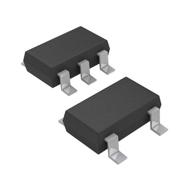
EL5120 is available in the 5 Ld TSOT package. All feature a
standard operational amplifier pin out. These amplifiers are
specified for operation with an ambient and junction
temperature range of -40°C to +125°C.
• Electronics Games
• 12MHz -3dB Bandwidth
• Supply Voltage = 4.5V to 16.5V
• Low Supply Current (per Amplifier) = 500µA
• High Slew Rate = 10V/µs
• Unity-Gain Stable
• Beyond the Rails Input Capability
• Rail-to-Rail Output Swing
• Pb-Free Available (RoHS Compliant)
Applications
• TFT-LCD Drive Circuits
• Electronics Notebooks
• Touch-Screen Displays
• Personal Communication Devices
• Personal Digital Assistants (PDA)
• Portable Instrumentation
• Sampling ADC Amplifiers
• Wireless LANs
• Office Automation
• Active Filters
• ADC/DAC Buffer
FN7186 Rev 8.00
October 15, 2015
Page 1 of 21
�EL5120, EL5220, EL5420
Ordering Information
PART NUMBER
(Note 3)
PART
MARKING
TEMP. RANGE
(°C)
PACKAGE
PKG. DWG. #
EL5120IWT-T7 (Notes 1, 4) (No longer K
available or supported)
-40 to +125
5 Ld TSOT Tape and Reel
MDP0049
EL5220ILZ-T13 (Notes 1, 2, 4) (No
longer available or supported)
20Z
-40 to +125
8 Ld DFN Tape and Reel (Pb-Free)
L8.2x3
EL5220CYZ (Note 2)
BBAAA
-40 to +125
8 Ld MSOP (Pb-Free)
MDP0043
EL5220CYZ-T7 (Notes 1, 2)
BBAAA
-40 to +125
8 Ld MSOP Tape and Reel (Pb-Free)
MDP0043
EL5220CYZ-T13 (Notes 1, 2)
BBAAA
-40 to +125
8 Ld MSOP Tape and Reel (Pb-Free)
MDP0043
EL5420CLZ (Note 2) (No longer
available or supported)
5420CLZ
-40 to +125
16 Ld QFN (Pb-Free)
MDP0046
EL5420CSZ (Note 2)
5420CSZ
-40 to +125
14 Ld SOIC (Pb-Free)
MDP0027
EL5420CSZ-T7 (Notes 1, 2)
5420CSZ
-40 to +125
14 Ld SOIC Tape and Reel (Pb-Free)
MDP0027
EL5420CSZ-T13 (Notes 1, 2)
5420CSZ
-40 to +125
14 Ld SOIC Tape and Reel (Pb-Free)
MDP0027
EL5420CR (Note 4) (No longer
available or supported)
5420CR
-40 to +125
14 Ld TSSOP
MDP0044
EL5420CRZ (Note 2)
5420CRZ
-40 to +125
14 Ld TSSOP (Pb-Free)
M14.173
EL5420CRZ-T7 (Notes 1, 2)
5420CRZ
-40 to +125
14 Ld TSSOP Tape and Reel (Pb-Free) M14.173
EL5420CRZ-T13 (Notes 1, 2)
5420CRZ
-40 to +125
14 Ld TSSOP Tape and Reel (Pb-Free) M14.173
NOTES:
1. Please refer to TB347 for details on reel specifications.
2. These Intersil Pb-free plastic packaged products employ special Pb-free material sets, molding compounds/die attach materials, and 100% matte
tin plate plus anneal (e3 termination finish, which is RoHS compliant and compatible with both SnPb and Pb-free soldering operations). Intersil
Pb-free products are MSL classified at Pb-free peak reflow temperatures that meet or exceed the Pb-free requirements of
IPC/JEDEC J STD-020.
3. For Moisture Sensitivity Level (MSL), please see device information page for EL5120, EL5220, EL5420. For more information on MSL please
see tech brief TB363.
4. Not recommended for new designs. Refer to EL5x20T for possible substitutions.
FN7186 Rev 8.00
October 15, 2015
Page 2 of 21
�EL5120, EL5220, EL5420
Pinouts
EL5220
(8 LD DFN)
TOP VIEW
EL5220
(8 LD MSOP)
TOP VIEW
8 VS+
VOUTA 1
7 VOUTB
VA
VIN+ 3 A
ER
NG
LO
NO
P
SU 5 VS+
LE
AB
IL + -
5 VINB+
EL5420
(14 LD TSSOP, SOIC)
TOP VIEW
VOUTA 1
VINA- 2
4 VIN-
14 VOUTD
- +
+ -
VINA+ 3
11 VS-
VINB+ 5
VOUTB 7
13 VIND12 VIND+
VS+ 4
VINB- 6
EL5420
(16 LD QFN)
TOP VIEW
10 VINC+
- +
+ -
9 VINC8 VOUTC
VINA- 1
VINA+ 2
VS+ 3
ER
VINB+ 4NG
O
L
NO
R
O
E
THERMAL
L
AB
LPAD
AI
V
A
13 NC
VS- 2
R
O
6 VINB-
VS- 4 ER
5 VINB+
NG
O
L
THERMAL PAD
NO
CONNECTS TO VS-
SU
ED
RT
O
PP 12 VIND-
11 VIND+
10 VS9 VINC+
VINC- 8
VOUT 1
ED
RT
O
P
VINA+ 3
14 VOUTD
EL5120
(5 LD TSOT)
TOP VIEW
+
7 VOUTB
VOUTC 7
VS- 4
6 VINB-
R
O
E
THERMAL
L
B
LAPAD
AI
V
A
15 VOUTA
VINA+ 3
VINA- 2
VOUTB 6
+
16 NC
VINA- 2
ED
RT
O
PP 8 VS+
SU
VINB- 5
VOUTA 1
THERMAL PAD
CONNECTS TO VS-
FN7186 Rev 8.00
October 15, 2015
Page 3 of 21
�EL5120, EL5220, EL5420
Absolute Maximum Ratings (TA = +25°C)
Thermal Information
Supply Voltage between VS+ and VS- . . . . . . . . . . . . . . . . . . . .+18V
Input Voltage . . . . . . . . . . . . . . . . . . . . . . . . . . VS- - 0.5V, VS +0.5V
Maximum Continuous Output Current . . . . . . . . . . . . . . . . . . . 30mA
Thermal Resistance (Typical)
JA (°C/W)
5 Ld TSOT (Note 5) . . . . . . . . . . . . . . . . . . . . . . . . .
214
8 Ld DFN (Note 6) . . . . . . . . . . . . . . . . . . . . . . . . . .
55
8 Ld MSOP (Note 5). . . . . . . . . . . . . . . . . . . . . . . . .
115
16 Ld QFN (Note 6) . . . . . . . . . . . . . . . . . . . . . . . . .
44
14 Ld SOIC (Note 5) . . . . . . . . . . . . . . . . . . . . . . . .
82
14 Ld TSSOP (Note 5) . . . . . . . . . . . . . . . . . . . . . . .
93
Storage Temperature . . . . . . . . . . . . . . . . . . . . . . . .-65°C to +150°C
Operating Junction Temperature Range . . . . . . . . . . -40°C to +125°
Power Dissipation . . . . . . . . . . . . . . . . . . . . . . . . . . . . . See Curves
Pb-Free Reflow Profile. . . . . . . . . . . . . . . . . . . . . . . . .see link below
http://www.intersil.com/pbfree/Pb-FreeReflow.asp
CAUTION: Do not operate at or near the maximum ratings listed for extended periods of time. Exposure to such conditions may adversely impact product reliability and
result in failures not covered by warranty.
NOTES:
5. JA is measured with the component mounted on a high effective thermal conductivity test board in free air. See Tech Brief TB379 for details.
6. JA is measured in free air with the component mounted on a high effective thermal conductivity test board with “direct attach” features. See
Tech Brief TB379.
IMPORTANT NOTE: All parameters having Min/Max specifications are guaranteed. Typ values are for information purposes only. Unless otherwise noted, all tests are
at the specified temperature and are pulsed tests, therefore: TJ = TC = TA
Electrical Specifications
PARAMETER
VS+ = +5V, VS- = -5V, RL = 10k and CL = 10pF to 0V, TA = +25°C, unless otherwise specified.
DESCRIPTION
CONDITIONS
MIN
TYP
MAX
12
UNIT
INPUT CHARACTERISTICS
VOS
Input Offset Voltage
VCM = 0V
2
TCVOS
Average Offset Voltage Drift
(Note 7)
5
IB
Input Bias Current
VCM = 0V
RIN
Input Impedance
2
mV
µV/°C
50
1
nA
G
CIN
Input Capacitance
CMIR
Common-Mode Input Range
1.35
CMRR
Common-Mode Rejection Ratio
for VIN from -5.5V to +5.5V
50
70
dB
AVOL
Open Loop Gain
-4.5V VOUT 4.5V
75
95
dB
-5.5
pF
+5.5
V
OUTPUT CHARACTERISTICS
VOL
Output Swing Low
IL = -5mA
-4.92
VOH
Output Swing High
IL = 5mA
4.92
V
ISC
Short Circuit Current
±120
mA
IOUT
Output Current
±30
mA
4.85
-4.85
V
POWER SUPPLY PERFORMANCE
PSRR
Power Supply Rejection Ratio
VS is moved from ±2.25V to ±7.75V
IS
Supply Current (Per Amplifier)
No load
60
500
80
-4.0V VOUT 4.0V, 20% to 80%
10
dB
750
µA
DYNAMIC PERFORMANCE
SR
Slew Rate (Note 8)
V/µs
tS
Settling to +0.1% (AV = +1)
(AV = +1), VO = 2V step
500
ns
BW
-3dB Bandwidth
RL = 10k, CL = 10pF
12
MHz
GBWP
Gain-Bandwidth Product
RL = 10k, CL = 10pF
8
MHz
PM
Phase Margin
RL = 10k, CL = 10pF
50
°
CS
Channel Separation
f = 5MHz (EL5220 and EL5420 only)
75
dB
NOTES:
7. Measured over operating temperature range.
8. Slew rate is measured on rising and falling edges.
FN7186 Rev 8.00
October 15, 2015
Page 4 of 21
�EL5120, EL5220, EL5420
Electrical Specifications
PARAMETER
VS+ = +5V, VS- = 0V, RL = 10k and CL = 10pF to 2.5V, TA = +25°C, unless otherwise specified.
DESCRIPTION
CONDITIONS
MIN
TYP
MAX
UNIT
10
mV
INPUT CHARACTERISTICS
VOS
Input Offset Voltage
VCM = 2.5V
2
TCVOS
Average Offset Voltage Drift
(Note 9)
5
IB
Input Bias Current
VCM = 2.5V
2
RIN
Input Impedance
1
G
CIN
Input Capacitance
1.35
pF
CMIR
Common-Mode Input Range
CMRR
Common-Mode Rejection Ratio
for VIN from -0.5V to +5.5V
45
66
dB
AVOL
Open Loop Gain
0.5V VOUT 4.5V
75
95
dB
-0.5
µV/°C
50
+5.5
nA
V
OUTPUT CHARACTERISTICS
VOL
Output Swing Low
IL = -5mA
VOH
Output Swing High
IL = +5mA
ISC
IOUT
80
4.85
150
mV
4.92
V
Short Circuit Current
±120
mA
Output Current
±30
mA
80
dB
POWER SUPPLY PERFORMANCE
PSRR
Power Supply Rejection Ratio
VS is moved from 4.5V to 15.5V
IS
Supply Current (Per Amplifier)
No load
500
60
750
µA
DYNAMIC PERFORMANCE
SR
Slew Rate (Note 10)
1V VOUT 4V, 20% to 80%
10
V/µs
tS
Settling to +0.1% (AV = +1)
(AV = +1), VO = 2V step
500
ns
BW
-3dB Bandwidth
RL = 10k, CL = 10pF
12
MHz
GBWP
Gain-Bandwidth Product
RL = 10k, CL = 10pF
8
MHz
PM
Phase Margin
RL = 10k, CL = 10pF
50
°
CS
Channel Separation
f = 5MHz (EL5220 and EL5420 only)
75
dB
NOTES:
9. Measured over operating temperature range.
10. Slew rate is measured on rising and falling edges.
FN7186 Rev 8.00
October 15, 2015
Page 5 of 21
�EL5120, EL5220, EL5420
Electrical Specifications
PARAMETER
VS+ = +15V, VS- = 0V, RL = 10k and CL = 10pF to 7.5V, TA = +25°C, unless otherwise specified.
DESCRIPTION
CONDITIONS
MIN
TYP
MAX
UNIT
14
mV
INPUT CHARACTERISTICS
VOS
Input Offset Voltage
VCM = 7.5V
2
TCVOS
Average Offset Voltage Drift
(Note 11)
5
IB
Input Bias Current
VCM = 7.5V
2
RIN
Input Impedance
1
G
CIN
Input Capacitance
1.35
pF
CMIR
Common-Mode Input Range
CMRR
Common-Mode Rejection Ratio
for VIN from -0.5V to +15.5V
53
72
dB
AVOL
Open Loop Gain
0.5V VOUT 14.5V
75
95
dB
-0.5
µV/°C
50
+15.5
nA
V
OUTPUT CHARACTERISTICS
VOL
Output Swing Low
IL = -5mA
VOH
Output Swing High
IL = +5mA
ISC
IOUT
80
14.85
150
mV
14.92
V
Short Circuit Current
±120
mA
Output Current
±30
mA
80
dB
POWER SUPPLY PERFORMANCE
PSRR
Power Supply Rejection Ratio
VS is moved from 4.5V to 15.5V
IS
Supply Current (Per Amplifier)
No load
500
60
750
µA
DYNAMIC PERFORMANCE
SR
Slew Rate (Note 12)
1V VOUT 14V, 20% to 80%
10
V/µs
tS
Settling to +0.1% (AV = +1)
(AV = +1), VO = 2V step
500
ns
BW
-3dB Bandwidth
RL = 10k, CL = 10pF
12
MHz
GBWP
Gain-Bandwidth Product
RL = 10k, CL = 10pF
8
MHz
PM
Phase Margin
RL = 10k, CL = 10pF
50
°
CS
Channel Separation
f = 5MHz (EL5220 and EL5420 only)
75
dB
NOTES:
11. Measured over operating temperature range
12. Slew rate is measured on rising and falling edges
FN7186 Rev 8.00
October 15, 2015
Page 6 of 21
�EL5120, EL5220, EL5420
Typical Performance Curves
1600
TYPICAL
PRODUCTION
DISTRIBUTION
1400
1200
1000
800
600
400
200
50
40
30
20
10
INPUT BIAS CURRENT (nA)
INPUT OFFSET VOLTAGE (mV)
5
0
-5
50
100
2.0
-50
4.95
4.94
50
100
150
TEMPERATURE (°C)
FIGURE 5. OUTPUT HIGH VOLTAGE vs TEMPERATURE
FN7186 Rev 8.00
October 15, 2015
0
50
100
21
19
150
FIGURE 4. INPUT BIAS CURRENT vs TEMPERATURE
-4.91
OUTPUT LOW VOLTAGE (V)
OUTPUT HIGH VOLTAGE (V)
4.96
0
17
-2.0
TEMPERATURE (°C)
VS = ±5V
IOUT = 5mA
-50
15
0.0
150
FIGURE 3. INPUT OFFSET VOLTAGE vs TEMPERATURE
4.93
13
VS = ±5V
TEMPERATURE (°C)
4.97
11
FIGURE 2. EL5420 INPUT OFFSET VOLTAGE DRIFT
VS = ±5V
0
9
INPUT OFFSET VOLTAGE DRIFT, TCVOS (µV/°C)
FIGURE 1. EL5420 INPUT OFFSET VOLTAGE DISTRIBUTION
-50
7
1
12
8
10
6
4
2
-0
-2
-4
-6
-8
-10
-12
INPUT OFFSET VOLTAGE (mV)
5
0
0
10
TYPICAL
PRODUCTION
DISTRIBUTION
VS = ±5V
60
3
QUANTITY (AMPLIFIERS)
VS = ±5V
TA = +25°C
QUANTITY (AMPLIFIERS)
70
1800
-4.92
VS = ±5V
IOUT = -5mA
-4.93
-4.94
-4.95
-4.96
-4.97
-50
0
50
100
150
TEMPERATURE (°C)
FIGURE 6. OUTPUT LOW VOLTAGE vs TEMPERATURE
Page 7 of 21
�EL5120, EL5220, EL5420
Typical Performance Curves
VS = ±5V
RL = 10k
10.40
SLEW RATE (V/µs)
100
OPEN LOOP GAIN (dB)
(Continued)
90
80
VS = ±5V
10.35
10.30
10.25
-50
0
50
100
-50
150
100
150
TEMPERATURE (°C)
TEMPERATURE (°C)
FIGURE 8. SLEW RATE vs TEMPERATURE
FIGURE 7. OPEN LOOP GAIN vs TEMPERATURE
700
VS = ±5V
TA = +25°C
0.55
SUPPLY CURRENT (µA)
SUPPLY CURRENT (mA)
50
0
0.5
600
500
400
0.45
-50
0
50
100
300
150
5
0
TEMPERATURE (°C)
FIGURE 9. EL5420 SUPPLY CURRENT PER AMPLIFIER vs
TEMPERATURE
5
-30
100
-80
-130
50
-50
10
100
1k
10k
PHASE (°)
GAIN (dB)
PHASE
-180
GAIN
-230
100k
1M
10M
100M
FREQUENCY (Hz)
FIGURE 11. OPEN LOOP GAIN AND PHASE vs FREQUENCY
FN7186 Rev 8.00
October 15, 2015
MAGNITUDE (NORMALIZED) (dB)
150
VS = ±5V, TA = +25°C
RL = 10k to GND
CL = 12pF to GND
20
15
FIGURE 10. EL5420 SUPPLY CURRENT PER AMPLIFIER vs
SUPPLY VOLTAGE
20
200
0
10
SUPPLY VOLTAGE (V)
10k
0
1k
560
-5
-10
150
CL = 10pF
AV = 1
VS = ±5V
-15
100k
1M
10M
100M
FREQUENCY (Hz)
FIGURE 12. FREQUENCY RESPONSE FOR VARIOUS RL
Page 8 of 21
�EL5120, EL5220, EL5420
Typical Performance Curves
(Continued)
200
RL = 10k
AV = 1
10 VS = ±5V
OUTPUT IMPEDANCE ()
MAGNITUDE (NORMALIZED) (dB)
20
12pF
0
50pF
-10
100pF
1000pF
-20
-30
100k
1M
160
120
80
40
0
10k
100M
10M
AV = 1
VS = ±5V
TA = +25°C
FIGURE 13. FREQUENCY RESPONSE FOR VARIOUS CL
FIGURE 14. CLOSED LOOP OUTPUT IMPEDANCE vs
FREQUENCY
80
12
10
60
8
CMRR (dB)
MAXIMUM OUTPUT SWING (VP-P)
10M
FREQUENCY (Hz)
FREQUENCY (Hz)
6
VS = ±5V
TA = +25°C
AV = 1
RL = 10k
CL = 12pF
Distortion


 工商网监
湘ICP备2023018690号
工商网监
湘ICP备2023018690号
