DATASHEET
EL5160, EL5161, EL5260, EL5261, EL5360
FN7387
Rev 11.00
August 11, 2015
200MHz Low-Power Current Feedback Amplifiers
The EL5160, EL5161, EL5260, EL5261, and EL5360 are
current feedback amplifiers with a bandwidth of 200MHz and
operate from just 0.75mA supply current. This makes these
amplifiers ideal for today’s high speed video and monitor
applications.
Features
With the ability to run from a single supply voltage from
5V to 10V, these amplifiers are ideal for handheld, portable, or
battery-powered equipment.
• Single and dual supply operation, from 5V to 10V supply span
• 200MHz -3dB bandwidth
• 0.75mA supply current
• 1700V/µs slew rate
• Fast enable/disable (EL5160, EL5260 and EL5360 only)
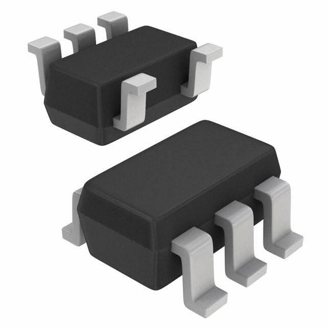
• Available in SOT-23 packages
The EL5160, EL5260, and EL5360 also incorporate an enable
and disable function to reduce the supply current to 14µA
typical per amplifier. Allowing the CE pin to float or applying a
low logic level enables the corresponding amplifier.
• Pb-Free (RoHS compliant)
Applications
• Battery-powered equipment
The EL5160 is available in the 6 Ld SOT-23 and 8 Ld SOIC
packages, the EL5161 in 5 Ld SOT-23 package, the EL5260 in
the 10 Ld MSOP package, the EL5261 in 8 Ld SOIC package,
the EL5360 in 16 Ld SOIC and QSOP packages. All operate
over the industrial temperature range of -40°C to +85°C.
• Handheld, portable devices
• Video amplifiers
• Cable drivers
• RGB amplifiers
• Test equipment
• Instrumentation
• Current-to-voltage converters
Pinouts
NC 1
IN- 2
+
IN+ 3
VS- 4
8 CE
OUT 1
7 VS+
VS- 2
6 OUT
IN+ 3
OUT 1
IN+ 3
+ -
6 VS+
OUT 1
5 CE
VS- 2
4 IN-
IN+ 3
5 VS+
+ 4 IN-
5 NC
+
VS- 4
CE 5
+
EL5360
(16 LD SOIC, QSOP)
TOP VIEW
EL5261
(8 LD SOIC)
TOP VIEW
EL5260
(10 LD MSOP)
TOP VIEW
IN- 2
EL5161
(5 LD SOT-23)
TOP VIEW
EL5160
(6 LD SOT-23)
TOP VIEW
EL5160
(8 LD SOIC)
TOP VIEW
10 VS+
OUTA 1
9 OUT
INA- 2
8 IN-
INA+ 3
7 IN+
VS- 4
6 CE
+
+
8 VS+
INA+ 1
7 OUTB
CEA 2
6 INB-
VS- 3
5 INB+
CEB 4
16 INA+
14 VS+
+
-
INB+ 5
INC+ 8
FN7387 Rev 11.00
August 11, 2015
13 OUTB
12 INB-
NC 6
CEC 7
15 OUTA
11 NC
+
-
10 OUTC
9 INC-
Page 1 of 17
�EL5160, EL5161, EL5260, EL5261, EL5360
Ordering Information
PART NUMBER
(Notes 2, 3)
PART MARKING
PACKAGE
(Pb-free)
TAPE & REEL
PKG.
DWG. #
EL5160ISZ
5160ISZ
-
8 Ld SOIC (150 mil)
M8.15E
EL5160ISZ-T7 (Note 1)
5160ISZ
7”
8 Ld SOIC (150 mil)
M8.15E
EL5160ISZ-T7A (Note 1)
5160ISZ
7”
8 Ld SOIC (150 mil)
M8.15E
EL5160ISZ-T13 (Note 1)
5160ISZ
13”
8 Ld SOIC (150 mil)
M8.15E
EL5160IWZ-T7 (Note 1)
BAAN (Note 4)
7” (3k pcs)
6 Ld SOT-23
P6.064A
EL5160IWZ-T7A (Note 1)
BAAN (Note 4)
7” (250 pcs)
6 Ld SOT-23
P6.064A
EL5161IWZ-T7 (Note 1)
BAJA (Note 4)
7” (3k pcs)
5 Ld SOT-23
P6.064A
EL5161IWZ-T7A (Note 1)
BAJA (Note 4)
7” (250 pcs)
5 Ld SOT-23
P6.064A
EL5260IYZ
(No longer available or supported)
BAAAK
-
10 Ld MSOP (3.0mm)
M10.118A
EL5260IYZ-T7 (Note 1)
(No longer available or supported)
BAAAK
7”
10 Ld MSOP (3.0mm)
M10.118A
EL5260IYZ-T13 (Note 1)
(No longer available or supported)
BAAAK
13”
10 Ld MSOP (3.0mm)
M10.118A
EL5261ISZ
(No longer available or supported)
5261ISZ
-
8 Ld SOIC (150 mil)
M8.15E
EL5261ISZ-T7 (Note 1)
(No longer available or supported)
5261ISZ
7”
8 Ld SOIC (150 mil)
M8.15E
EL5261ISZ-T13 (Note 1)
(No longer available or supported)
5261ISZ
13”
8 Ld SOIC (150 mil)
M8.15E
EL5360ISZ
(No longer available or supported)
EL5360ISZ
-
16 Ld SOIC (150 mil)
MDP0027
EL5360ISZ-T7 (Note 1)
(No longer available or supported)
EL5360ISZ
7”
16 Ld SOIC (150 mil)
MDP0027
EL5360ISZ-T13 (Note 1)
(No longer available or supported)
EL5360ISZ
13”
16 Ld SOIC (150 mil)
MDP0027
EL5360IUZ(No longer available or
supported)
5360IUZ
-
16 Ld QSOP (150 mil)
MDP0040
EL5360IUZ-T7 (Note 1)
(No longer available or supported)
5360IUZ
7”
16 Ld QSOP (150 mil)
MDP0040
EL5360IUZ-T13 (Note 1)
(No longer available or supported)
5360IUZ
13”
16 Ld QSOP (150 mil)
MDP0040
NOTES:
1. Please refer to TB347 for details on reel specifications.
2. Intersil Pb-free plus anneal products employ special Pb-free material sets; molding compounds/die attach materials and 100% matte tin plate
termination finish, which are RoHS compliant and compatible with both SnPb and Pb-free soldering operations. Intersil Pb-free products are MSL
classified at Pb-free peak reflow temperatures that meet or exceed the Pb-free requirements of IPC/JEDEC J STD-020.
3. For Moisture Sensitivity Level (MSL), please see product information page for EL5160, EL5161, EL5260, EL5261, EL5360. For more information on
MSL, please see tech brief TB363.
4. The part marking is located on the bottom of the part.
FN7387 Rev 11.00
August 11, 2015
Page 2 of 17
�EL5160, EL5161, EL5260, EL5261, EL5360
3
Absolute Maximum Ratings (TA = +25°C)
Thermal Information
Supply Voltage between VS+ and VS-. . . . . . . . . . . . . . . . . . . . . . . . . . 13.2V
Maximum Continuous Output Current . . . . . . . . . . . . . . . . . . . . . . . . . 50mA
Slew Rate of VS+ to VS- . . . . . . . . . . . . . . . . . . . . . . . . . . . . . . . . . . . . . 1V/µs
Pin Voltages. . . . . . . . . . . . . . . . . . . . . . . . . . . . . (VS-) - 0.5V to (VS+) + 0.5V
Maximum Operating Junction Temperature . . . . . . . . . . . . . . . . . . +125°C
Maximum Power Dissipation . . . . . . . . . . . . . . . . . . . see curves on page 7
Maximum Storage Temperature Range . . . . . . . . . . . . . -65°C to +150°C
Ambient Operating Temperature Range . . . . . . . . . . . . . . -40°C to +85°C
Pb-free reflow profile . . . . . . . . . . . . . . . . . . . . . . . . . . . . . . . . see link below
http://www.intersil.com/pbfree/Pb-FreeReflow.asp
CAUTION: Stresses above those listed in “Absolute Maximum Ratings” may cause permanent damage to the device. This is a stress only rating and
operation of the device at these or any other conditions above those indicated in the operational sections of this specification is not implied.
Electrical Specifications VS+ = +5V, VS- = -5V, RF = 750Ω for AV = 1, RL = 150Ω, VCE, H = VS+, VCE, L = (VS+) -3V, TA = +25°C, Unless
Otherwise Specified. Boldface limits apply across the operating temperature range, -40°C to +85°C.
PARAMETER
DESCRIPTION
CONDITIONS
MIN
(Note 6)
TYP
MAX
(Note 6)
UNIT
AC PERFORMANCE
BW
-3dB Bandwidth
AV = +1, RL = 500Ω
200
MHz
AV = +2, RL = 150Ω
125
MHz
10
MHz
BW1
0.1dB Bandwidth
RL = 100Ω
SR
Slew Rate
VO = -2.5V to +2.5V, AV = +2, RF = RG = 1kΩ,
RL = 100Ω
900
1700
2500
V/µs
EL5260, EL5261
800
1300
2500
V/µs
SR
500Ω Load
1360
V/µs
tS
0.1% Settling Time
35
ns
eN
Input Voltage Noise
4
nV/√Hz
iN-
IN- Input Current Noise
7
pA/√Hz
iN+
IN+ Input Current Noise
8
pA/√Hz
VOUT = -2.5V to +2.5V, AV = +2
HD2
5MHz, 2.5VP-P, RL = 150Ω, AV = +2
-74
dBc
HD3
5MHz, 2.5VP-P, RL = 150Ω, AV = +2
-50
dBc
dG
Differential Gain Error (Note 5)
AV = +2
0.1
%
dP
Differential Phase Error (Note 5)
AV = +2
0.1
°
DC PERFORMANCE
VOS
Offset Voltage
TCVOS
Input Offset Voltage Temperature
Coefficient
Measured from TMIN to TMAX
ROL
Open Loop Transimpedance Gain
±2.5VOUT into 150Ω
-5
1.6
+5
mV
6
µV/°C
800
2000
kΩ
V
INPUT CHARACTERISTICS
CMIR
Common Mode Input Range
Guaranteed by CMRR test
±3
±3.3
CMRR
Common Mode Rejection Ratio
VIN = ±3V
50
62
-ICMR
- Input Current Common Mode Rejection
+IIN
75
dB
-1
+1
µA/V
+ Input Current
-4
+4
µA
-IIN
- Input Current
-5
+5
µA
RIN
Input Resistance
15
MΩ
CIN
Input Capacitance
FN7387 Rev 11.00
August 11, 2015
1.5
4
1
pF
Page 3 of 17
�EL5160, EL5161, EL5260, EL5261, EL5360
Electrical Specifications VS+ = +5V, VS- = -5V, RF = 750Ω for AV = 1, RL = 150Ω, VCE, H = VS+, VCE, L = (VS+) -3V, TA = +25°C, Unless
Otherwise Specified. Boldface limits apply across the operating temperature range, -40°C to +85°C. (Continued)
MIN
(Note 6)
TYP
MAX
(Note 6)
UNIT
RL = 150Ω to GND
±3.1
±3.4
±3.8
V
RL = 1kΩ to GND
±3.8
±4.0
±4.2
V
Output Current
RL = 10Ω to GND
40
70
140
mA
Supply Current - Enabled, per Amplifier
No load, VIN = 0V (EL5160, EL5161, EL5260,
EL5261)
0.6
0.75
0.85
mA
No load, VIN = 0V (EL5360)
0.6
0.8
0.92
mA
0
10
25
µA
-25
-14
0
µA
PARAMETER
DESCRIPTION
CONDITIONS
OUTPUT CHARACTERISTICS
VO
Output Voltage Swing
IOUT
SUPPLY
ISON
ISOFF+
Supply Current - Disabled, per Amplifier
No load, VIN = 0V, Only EL5160, EL5260,
EL5360
ISOFF-
Supply Current - Disabled, per Amplifier
PSRR
Power Supply Rejection Ratio
DC, VS = ±4.75V to ±5.25V
65
74
-IPSR
- Input Current Power Supply Rejection
DC, VS = ±4.75V to ±5.25V
-0.5
0.1
dB
0.5
µA/V
ENABLE (EL5160, EL5260, EL5360 ONLY)
tEN
Enable Time
600
ns
tDIS
Disable Time
800
ns
ICE, H
CE Pin Input High Current
CE = VS+
1
5
25
µA
ICE, L
CE Pin Input Low Current
CE = (VS+) - 5V
-1
0
1
µA
NOTE:
5. Standard NTSC test, AC signal amplitude = 286mVP-P, f = 3.58MHz.
6. Compliance to datasheet limits is assured by one or more methods: production test, characterization and/or design.
3
4
1
2
NORMALIZED GAIN (dB)
NORMALIZED GAIN (dB)
Typical Performance Curves
-1
-3 V = +5V
S+
VS- = -5V
RL = 150Ω
-5 A = 2
V
RF = 806Ω
RG = 806Ω
-7
100k
1M
10M
100M
FREQUENCY (Hz)
FIGURE 1. FREQUENCY RESPONSE (AV = +2)
FN7387 Rev 11.00
August 11, 2015
1G
0
-2
VS+ = +5V
VS- = -5V
-4 AV = 1
RL = 500Ω
RF = 2800Ω
-6
100k
1M
10M
100M
1G
FREQUENCY (Hz)
FIGURE 2. FREQUENCY RESPONSE (AV = +1)
Page 4 of 17
�EL5160, EL5161, EL5260, EL5261, EL5360
Typical Performance Curves
(Continued)
4
RL = 500Ω
RF = 2.7kΩ
3 AV = 1
NORMALIZED GAIN (dB)
NORMALIZED GAIN (dB)
5
±5V
1
±6V
±4V
-1
±3V
±2.5V
-3
-5
100k
1M
10M
100M
AV = 2
RL=150Ω
2 RF = RG = 762Ω
±5V
0
±4V
-2
±3V
±6V
±2.5V
-4
-6
100k
1G
1M
10M
FREQUENCY (Hz)
FIGURE 4. FREQUENCY RESPONSE FOR VARIOUS
SUPPLY VOLTAGES
VS+ = +5V
VS- = -5V
AV = 10
RL = 500Ω
RF = 560Ω
2
0
-2
-4
10M
100M
1G
10M
TRANSIMPEDANCE (Ω)
NORMALIZED GAIN (dB)
4
1M
1M
100k
10k
1k
100
10
1k
10k
100k
FREQUENCY (Hz)
FIGURE 5. FREQUENCY RESPONSE (AV = +10)
INPUT
1V/DIV
OUTPUT
500mV/DIV
VS+ = +5V
VS- = -5V
AV = 2
RL = 150Ω
RF = RG = 422Ω
4ns/DIV
FIGURE 7. OUTPUT RISE TIME
FN7387 Rev 11.00
August 11, 2015
1G
FREQUENCY (Hz)
FIGURE 3. FREQUENCY RESPONSE FOR VARIOUS ±VS
-6
100k
100M
1M
10M
100M
1G
FREQUENCY (Hz)
FIGURE 6. OPEN LOOP TRANSIMPEDANCE GAIN vs FREQUENCY
(ROL)
OUTPUT
500mV/DIV
INPUT
1V/DIV
VS+ = +5V
VS- = -5V
AV = 2
RL = 150Ω
RF = RG = 422Ω
4ns/DIV
FIGURE 8. OUTPUT FALL TIME
Page 5 of 17
�EL5160, EL5161, EL5260, EL5261, EL5360
Typical Performance Curves
VS+ = +5V
VS- = -5V
(Continued)
CE
5V/DIV
5V/DIV
CE
200mV/DIV
VOUT
200mV/DIV
VOUT
VS+ = +5V
VS- = -5V
400ns/DIV
400ns/DIV
FIGURE 9. DISABLE DELAY TIME
1K
VS+ = +5V
VS- = -5V
OUTPUT IMPEDANCE (Ω)
0
FIGURE 10. ENABLE DELAY TIME
PSRR (dB)
-20
-40
VS+
-60
VS-
-80
-100
1k
10k
100k
1M
10M
100M
VS+ = +5V
VS- = -5V
100
10
1
100m
10m
10k
1G
100k
FREQUENCY (Hz)
100M
FIGURE 12. CLOSED LOOP OUTPUT IMPEDANCE vs FREQUENCY
4
4
VS = ±5V
RG = 750Ω
2 RL = 150Ω
NORMALIZED GAIN (dB)
NORMALIZED GAIN (dB)
10M
FREQUENCY (Hz)
FIGURE 11. PSRR vs FREQUENCY
0
AV = -2
-2
1M
AV = -5
AV = +2
-4
VS = ±5V
AV = -1
2 RL = 150Ω
RF = 768Ω
0
RF = 1kΩ
-2
RF = 1.2kΩ
-4
RF = 1.5kΩ
-6
100k
1M
10M
100M
1G
FREQUENCY (Hz)
FIGURE 13. FREQUENCY RESPONSE FOR VARIOUS GAIN
SETTINGS
FN7387 Rev 11.00
August 11, 2015
-6
100k
1M
10M
100M
1G
FREQUENCY (Hz)
FIGURE 14. FREQUENCY RESPONSE FOR VARIOUS FEEDBACK
RESISTORS, AV = -1
Page 6 of 17
�EL5160, EL5161, EL5260, EL5261, EL5360
Typical Performance Curves
(Continued)
5
VS = ±5V
RF = 768Ω
2 RL = 500Ω
AV = -5
NORMALIZED GAIN (dB)
NORMALIZED GAIN (dB)
4
AV = -1
0
AV = +5
-2
AV = +10
-4
-6
100k
1M
10M
100M
VS = ±5V
AV = +1
3 RL = 150Ω
RF = 1kΩ
1
RF = 2.8kΩ
-1
-3
-5
100k
1G
1M
FREQUENCY (Hz)
1.250W
POWER DISSIPATION (W)
POWER DISSIPATION (W)
1.4
1.2
SO16 (0.150”)
JA = 80°C/W
0.8
SO8
JA = 110°C/W
0.6
435mW
0.4
SOT23-5/6
JA = 110°C/W
0.2
0
0
25
50
75 85 100
125
1.2
1 893mW
0.8 870mW
MSOP10
JA=115°C/W
0.4
0.2
0
25
1.2
SO16 (0.150”)
JA = 110°C/W
0.7
0.6
SO8
JA = 160°C/W
625mW
0.5
0.4
391mW
0.3
0.2
SOT23-5/6
JA = 256°C/W
0.1
0
25
50
75 85 100
125
150
FREQUENCY (Hz)
FIGURE 19. PACKAGE POWER DISSIPATION vs AMBIENT
TEMPERATURE
FN7387 Rev 11.00
August 11, 2015
125
150
JEDEC JESD51-3 LOW EFFECTIVE THERMAL
CONDUCTIVITY TEST BOARD
1
0.8
633mW
0.6
486mW
QSOP16
JA = 158°C/W
0.4
MSOP10
JA = 206°C/W
0.2
0
0
75 85 100
FIGURE 18. PACKAGE POWER DISSIPATION vs AMBIENT
TEMPERATURE
POWER DISSIPATION (W)
POWER DISSIPATION (W)
909mW
50
FREQUENCY (Hz)
JEDEC JESD51-3 LOW EFFECTIVE THERMAL
CONDUCTIVITY TEST BOARD
0.8
QSOP16
JA=112°C/W
0.6
0
150
FIGURE 17. PACKAGE POWER DISSIPATION vs AMBIENT
TEMPERATURE
1
1G
JEDEC JESD51-7 HIGH EFFECTIVE THERMAL
CONDUCTIVITY TEST BOARD
FREQUENCY (Hz)
0.9
100M
FIGURE 16. FREQUENCY RESPONSE FOR VARIOUS FEEDBACK
RESISTORS, AV = +1
JEDEC JESD51-7 HIGH EFFECTIVE THERMAL
CONDUCTIVITY TEST BOARD
1 909mW
10M
FREQUENCY (Hz)
FIGURE 15. FREQUENCY RESPONSE FOR VARIOUS GAIN
SETTINGS
1.4
RF = 750Ω
0
25
50
75 85 100
125
150
FREQUENCY (Hz)
FIGURE 20. PACKAGE POWER DISSIPATION vs AMBIENT
TEMPERATURE
Page 7 of 17
�EL5160, EL5161, EL5260, EL5261, EL5360
Pin Descriptions
EL5160
(8 Ld SOIC)
EL5160
(6 Ld SOT-23)
EL5161
EL5260
EL5261
EL5360
PIN
NAME
1, 5
-
-
-
-
6, 11
NC
Not connected
2
4
4
2, 8
2, 6
9, 12, 16
IN-
Inverting input
FUNCTION
EQUIVALENT CIRCUIT
VS+
IN+
IN-
VSCircuit 1
3
3
3
3, 7
3, 5
1, 5, 8
IN+
Non-inverting input
4
2
2
4
4
3
VS-
Negative supply
6
1
1
1, 9
1, 7
10, 13, 15
OUT
Output
(See circuit 1)
VS+
OUT
VSCircuit 2
7
6
5
10
8
14
VS+
Positive supply
8
5
-
5, 6
-
2, 4, 7
CE
Chip enable
VS+
CE
VSCircuit 3
Applications Information
Product Description
The EL5160, EL5161, EL5260, EL5261, and EL5360 are low
power, current-feedback operational amplifiers that offer a wide
-3dB bandwidth of 200MHz and a low supply current of 0.75mA
per amplifier. The EL5160, EL5161, EL5260, EL5261, and
EL5360 work with supply voltages ranging from a single 5V to
10V and they are also capable of swinging to within 1V of either
supply on the output. Because of their current-feedback topology,
the EL5160, EL5161, EL5260, EL5261, and EL5360 do not
have the normal gain-bandwidth product associated with
voltage-feedback operational amplifiers. Instead, their -3dB
bandwidth remains relatively constant as closed-loop gain is
increased. This combination of high bandwidth and low power,
together with aggressive pricing make the EL5160, EL5161,
EL5260, EL5261, and EL5360 ideal choices for many
low-power/high-bandwidth applications such as portable,
handheld, or battery-powered equipment.
FN7387 Rev 11.00
August 11, 2015
Power Supply Bypassing and Printed Circuit
Board Layout
As with any high frequency device, good printed circuit board
layout is necessary for optimum performance. Low impedance
ground plane construction is essential. Surface mount
components are recommended, but if leaded components are
used, lead lengths should be as short as possible. The power
supply pins must be well bypassed to reduce the risk of
oscillation. The combination of a 4.7µF tantalum capacitor in
parallel with a 0.01µF capacitor has been shown to work well
when placed at each supply pin.
For good AC performance, parasitic capacitance should be kept
to a minimum, especially at the inverting input. (See the
“Capacitance at the Inverting Input” section) Even when ground
plane construction is used, it should be removed from the area
near the inverting input to minimize any stray capacitance at that
node. Carbon or Metal-Film resistors are acceptable with the
Metal-Film resistors giving slightly less peaking and bandwidth
because of additional series inductance. Use of sockets,
particularly for the SO package, should be avoided if possible.
Sockets add parasitic inductance and capacitance which results
in additional peaking and overshoot.
Page 8 of 17
�EL5160, EL5161, EL5260, EL5261, EL5360
Disable/Power-Down
The EL5160, EL5260, EL5360 amplifiers can be disabled,
placing the output in a high impedance state. When disabled, the
amplifier supply current reduces to


 工商网监
湘ICP备2023018690号
工商网监
湘ICP备2023018690号
